DOI:
10.1039/C6RA26171J
(Paper)
RSC Adv., 2017,
7, 3704-3712
Domain and antiferroelectric properties of Pb(Lu1/2Nb1/2)O3 single crystals and their superlattice structure
Received
2nd November 2016
, Accepted 26th December 2016
First published on 13th January 2017
Abstract
In order to obtain antiferroelectric single crystals for understanding their structure and the physics and chemistry of the antiferroelectric phenomenon, antiferroelectric single crystals of Pb(Lu1/2Nb1/2)O3 (PLN) were successfully grown. Two sets of superlattice reflections including the B-site atom ordering type reflection and the lead-ion antiparallel ordering type reflection were confirmed and distinguished from the X-ray diffraction patterns and transmission electron microscopy. Micro-domains and macro-domains were observed under the microscopes. The investigations were focused on the extinction angle, the angle of the domain wall and temperature dependence. The Curie temperature TC was about 240 °C and 254 °C for [111]-oriented and [001]-oriented crystal plates respectively. The value of the energy density was calculated to be 3.65 J cm−3 for the [111]-oriented sample at 200 °C based on the double hysteresis loops with an electric field EAPP = 170 kV cm−1 applied. All the above features, especially the high Curie temperature and high energy storage density, suggested that the PLN single crystals should be useful for large size energy storage devices that require a wider operation temperature range.
1. Introduction
An antiferroelectric state is defined as one in which lines of ions in the crystal are spontaneously polarized, but with neighboring lines polarized in antiparallel directions.1 Among the numerous antiferroelectrics with perovskite structure, a typical and one of the most widely studied antiferroelectric compositions is PbZrO3.2,3 Pb(Zr1−xTix)O3 (PZT) with low Ti-content (x < 0.05) is an antiferroelectric material at room temperature and has drawn much attention among physics and material science researchers owing to its technological importance and complex phase diagram.3,4 Recently, a number of investigations based on La3+ and Sn4+ modified PZT ceramics and thin films were reported.5–8 On the other hand, compounds of ABO3 including A(B′1/2B′′1/2)O3 and (A′1/2A′′1/2)BO3, as an another class of antiferroelectric materials, have recently attracted much research interest.9–12 Especially, a group of complex lead-based perovskite oxides with chemical formula Pb(B′xB′′1−x)O3 have considerable interest due to their variety of physical properties and wide range of applications such as high-energy density storage capacitors.9 Pb(Mg1/2W1/2)O3, Pb(Co1/2W1/2)O3 and Pb(Yb1/2Nb1/2)O3 are the well-known members of antiferroelectrics which belong to a subgroup of B-site atom ordering and a long coherence length of long-range ordering.10,11 Besides, the A-site complex perovskite compounds, such as (Na1/2Bi1/2)TiO3 (NBT)12 and (K1/2Na1/2)NbO3 (KNN)13 based solid solution were also studied.
As a member of Pb(B′1/2B′′1/2)O3 family, Pb(Lu1/2Nb1/2)O3 (PLN) have been received some attention in the past. The PLN ceramics were obtained with long range order parameter Ω close to unity, and a sharp antiferroelectric–paraelectric phase transition at about 258 °C in the absence of dielectric dispersion.10,14 Antonova M. et al. also reported the Pb(Lu1/2Nb1/2)O3–PbTiO3 (PLN–PT) ceramics system prepared by a hot-pressed routine method, a pure PLN was presented with long-range order in the B sublattice and an orthorhombic cell.15 Highly oriented PLN thin film heterostructures with bottom La1/2Sr1/2CoO3 (LSCO) and top Pt electrodes were deposited by pulsed laser deposition.16 At room temperature, Au/PLN/LSCO thin film heterostructures exhibit ferroelectric behaviors in contrast to typical antiferroelectric features of PLN ceramic.16 The lower degree of chemical ordering is considered to be the main reason.
Antiferroelectric crystals are promising candidates for dielectrics which are applied in high energy density electrical capacitors, especially for large size capacitor devices, due to the reversible electric field-induced antiferroelectric–ferroelectric phase transition.17–19 In addition, antiferroelectric crystals can be used for making some transparent block device which is applied to the optical system. However, until now most of study on antiferroelectric materials only focus on the form of ceramics or thin film due to the huge challenge of the growth of the antiferroelectric crystals. Even though much attention has been focused on modified PZ and PZT based single crystals, for example Pb(Zr,Ti)O3,4 (Pb,La)(Zr,Sn,Ti)O3 single crystals20–22 and so on. But the relevant reports on PLN-based AFE single crystal is still quite less until now and these intrigued us to grow the PLN AFE single crystals.23 Actually, compared with the ceramics or thin film, single crystal is an ideal object to investigate on the antiferroelectric phenomenon. As for the PLN materials, the inherent antiferroelectric properties are unclear due to deficiency of single crystal although PLN ceramics received much attention. Therefore, the investigation on PLN single crystals can help to understand not only the physics and chemistry of the antiferroelectric phenomenon, but also the potential application of PLN single crystals. In this paper, the investigation on the superlattice structure, domain and antiferroelectric properties of PLN single crystals was reported.
2. Experimental section
2.1 Crystal growth
Due to the high melting point of Lu2O3, a high-temperature solution technique24 was chosen to grow PLN single crystals by means of adding flux to decrease the growing temperature as low as possible. The starting chemicals, PbO (99.9%), Lu2O3 (99.99%), Nb2O5 (99.9%) and H3BO3 (99.9%), were weighed according to the different ratios of flux to solute in order to realize the optimization of PLN crystal growth process. The proper flux/PLN molar ratio was 6.5![[thin space (1/6-em)]](https://www.rsc.org/images/entities/char_2009.gif) :1 with a molar ratio of 8:1 for PbO/H3BO3 after many trials. Mixtures were placed into Pt crucibles, then the crucibles were carried out in a muffle furnace equipped with an automatic temperature controller. The thermal program used for the spontaneous nucleation growth of PLN crystals were controlled by various thermal profiles, namely: (i) heating from room temperature to 1080 °C at a ramp rate of 100 °C h−1 and dwelling for 24 h; (ii) slow cooling from 1080 °C to 1050 °C at 5 °C h−1, from 1050 °C to 1030 °C at 0.1 °C h−1, from 1030 °C to 1000 °C at 0.2 °C h−1; (iii) cooling from 1000 °C down to room temperature at 100 °C h−1. The residual flux was dissolved using 30% hot HNO3 solutions, and the grown crystals were separated. Crystal seeds (of 2 × 2 × 5 mm3 in size) obtained from spontaneous nucleation growth were used for the top seeded solid solution growth (TSSG) method. Compared with other methods, the TSSG method also offers more advantages in growing single crystals of good quality and high compositional homogeneity due to its slow growth process. The detailed growth process is similar to the one described by C. He et al.25 and the saturation temperature Ts of the solution were determined to be about 1040 °C by repeated seeding trials. At the stage of growth, the slow cooling rate was set at 0.2 °C h−1. Finally, PLN single crystals were obtained as shown in Fig. 1.
:1 with a molar ratio of 8:1 for PbO/H3BO3 after many trials. Mixtures were placed into Pt crucibles, then the crucibles were carried out in a muffle furnace equipped with an automatic temperature controller. The thermal program used for the spontaneous nucleation growth of PLN crystals were controlled by various thermal profiles, namely: (i) heating from room temperature to 1080 °C at a ramp rate of 100 °C h−1 and dwelling for 24 h; (ii) slow cooling from 1080 °C to 1050 °C at 5 °C h−1, from 1050 °C to 1030 °C at 0.1 °C h−1, from 1030 °C to 1000 °C at 0.2 °C h−1; (iii) cooling from 1000 °C down to room temperature at 100 °C h−1. The residual flux was dissolved using 30% hot HNO3 solutions, and the grown crystals were separated. Crystal seeds (of 2 × 2 × 5 mm3 in size) obtained from spontaneous nucleation growth were used for the top seeded solid solution growth (TSSG) method. Compared with other methods, the TSSG method also offers more advantages in growing single crystals of good quality and high compositional homogeneity due to its slow growth process. The detailed growth process is similar to the one described by C. He et al.25 and the saturation temperature Ts of the solution were determined to be about 1040 °C by repeated seeding trials. At the stage of growth, the slow cooling rate was set at 0.2 °C h−1. Finally, PLN single crystals were obtained as shown in Fig. 1.
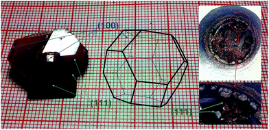 |
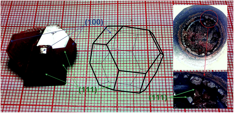
| | Fig. 1 As-grown PLN single crystals and sketch map for a tetrakaidecahedron combination. | |
2.2 Characterization
The phase and structure of the grown crystal were investigated by X-ray diffraction (XRD) analysis using Cu-Kα radiation (Ultima-IV, Rigaku, Japan) at room temperature. Powders X-ray diffraction was studied using ground and sieved powders sample. The scan step of 2θ is 0.02°, with an angular range of 10–80° and a rotating speed of 5° min−1. Moreover, fine crystal powder for the electron microscopy study was polished mechanically, which was dispersed in alcohol to form a dilute suspension. One droplet of the suspension was dropped onto a copper grid with carbon support film. All the investigations were performed on a transmission electron microscope (TEM) (Tecnai F20 FEG, FEI, America). A polarized light microscope (PLM) (LV100POL, Nikon, Japan) equipped with hot plate (THMS 600 E, Linkam, U.K.) was employed to determine the symmetry, domain structure and its evolution as the temperature of the as-grown crystal increases. The optical crystal plates were cut from as grown crystal along the [001] and [111] directions, which were then grinded and polished to 50 μm in thickness. For electric characterization, different thicknesses of plates were sliced from the as-grown crystals along the [001] and [111] directions. The samples were then polished and coated with silver paste as electrodes. Measurements of the dielectric constant (ε′) was carried out on samples by computer-controlled Alpha-broadband dielectric/impedance spectrometer (Novocontrol GmbH, Novocontrol, Germany) with an AC signal of 0.5 V (peak to peak) applied. Differential Scanning Calorimeter (DSC) was performed on differential thermal analysis apparatus (DTA 404 PC, NETZSCH, Germany), from room temperature to 1000 °C. Polarization hysteresis loops were displayed by standard ferroelectric test system (TF Analyzer 2000E, aix-ACCT, Germany) combined with a high-voltage supply amplifier/controller (Model 610E, Trek, America) and an environmental test chamber (DELTA 9023, DELTA, America) controlled from room temperature to 240 °C.
3. Results and discussion
3.1 Crystals
The photographs of the obtained PLN crystals are shown in Fig. 1. Compared with the size (2–6 mm) of the PLN crystals grown by spontaneous nucleation, the dimensions of the as-grown crystal obtained by TSSG method reached as large as 20 × 20 × 12 mm3. The chemical bonding theory of single crystal growth26,27 indicates that the micro structure of lattice planes corresponds to the anisotropic distribution of constituent bonding atoms governing crystal growth with particular rates. Compared with the configuration of PLN crystals, it was found that the (111) plane grew preferentially at the initial stage of crystal growth, and the (001) plane was generated gradually later as a result of the increase of the crystal size. External macro structure of the crystal was a tetrakaidecahedron combination with pseudocubic (111) and (001) planes in habit, and color of dark yellow as shown in Fig. 1.
3.2 Structure analysis
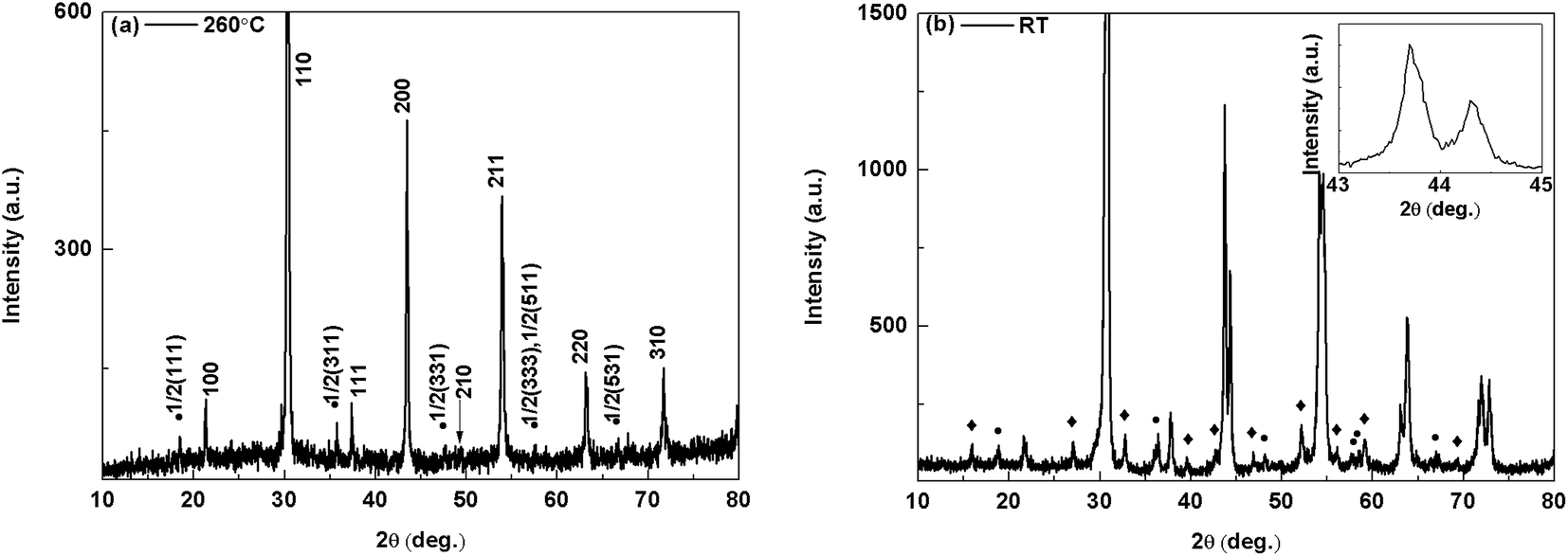
Powder X-ray diffraction patterns for PLN was measured at 260 °C and room temperature, showing perovskite structure as shown in Fig. 2. In addition, some superlattice reflections were found. Superlattice reflections might originate from three sources: long range ordering of B-site cations, antiparallel cation displacements and tilting of the BO6 octahedra.9 Due to the high structural stability of perovskite structured compounds,28 the two atom species are allowed to occupy at the B sites. Pure PLN has a pronounced long-range order in the B sublattice that arises from long range order of Lu3+ and Nb3+ cations. The structure adopts a doubled perovskite unit cell due to the A(B′1/2B′′1/2)O3-type ‘1:1’ ordering with a face-centered arrangement of two different (B′ and B′′) sublattices.29 Just above the transition temperature as shown in Fig. 2(a), the superlattice reflections as indicated by full circles only originate from the long-range ordering of Lu3+ and Nb3+ cations on the octahedral site of the perovskite lattice in addition to the fundamental reflections. These peaks corresponding to d-spacing values twice as much as those of (111), (311), (331), (333), and (531) major ones can be indexed as 1/2(111), 1/2(311), 1/2(331), 1/2(333), and 1/2(531), respectively, showing good order feature of a single crystal. The presence of superlattice reflection due to B-site atom ordering suggests that the prototypic crystal structure is an ordered perovskite with an effective unit cell (2ac × 2ac × 2ac) (c for cubic) doubled in size in all crystallographic axis directions of a cubic, simple perovskite cell (ac × ac × ac), in terms of crystallography, it means that B3+ and B5+ ions follow each other at distances.14
 |
| | Fig. 2 X-ray powder diffraction patterns of the crashed PLN crystal sample at (a) 260 °C and (b) room temperature; (◆) superlattice reflections due to antiparallel displacements of cation; (●) superlattice reflections due to B-site atom ordering. The split in the fundamental lines around 2θ = 44° inset in (b) clearly show the orthorhombic phase. | |
As evidenced from the split in the fundamental lines around 2θ = 44° of the low-temperature phase, shown in the insets of Fig. 2(b), the lattice distortion is found to be orthorhombic in nature.30 The unit cell of the room-temperature phase can be constructed from a primitive orthorhombic with lattice parameters ao = 4.156 Å, bo = 4.134 Å and co = 4.090 Å, where the subscript o refers to the orthorhombic lattice. The room-temperature XRD reveals complicated extra reflections as indicated by the full rhombus in Fig. 2(b), which appear only below the transition temperature. These extra reflects are most likely to originate from the antiparallel displacements of Pb2+ ions. Its crystal symmetry is similar to that of lead zirconate (PbZrO3) where the crystal structure is characterized by the antiparallel Pb2+ displacement.31
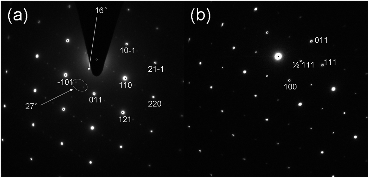
The superlattice reflections were further identified by transmission electron microscopy. Fig. 3(a) shows the electron diffraction pattern obtained in the [1−11] zone-axes, exhibiting the fundamental spots of the prototype and the extra superlattice spots. The superlattice spots contain two sets of superlattice spots (B-site atom ordering superlattice reflections and Pb2+ antiparallel displacements superlattice reflections). The superlattice spots of Pb2+ antiparallel displacements are confirmed by the spots around 2θ = 16°, 27° and others. The electron diffraction pattern [Fig. 3(b)] obtained in the [01−1] zone is composed of fundamental spots and the B-site atom ordering superlattice reflections. The superlattice spot is only the B-cation ordering observed in this zone in contrast to that shown in Fig. 3(a). It is also confirmed that the extra superlattice spots in Fig. 3(a) can be observed only along the orthorhombic ao direction. The agreement between the present XRD and high-resolution TEM investigations reveals the existence of a long-range superlattice resulted from orthorhombic symmetry. Therefore, the two sets of superlattice can be distinguished from structural analysis.
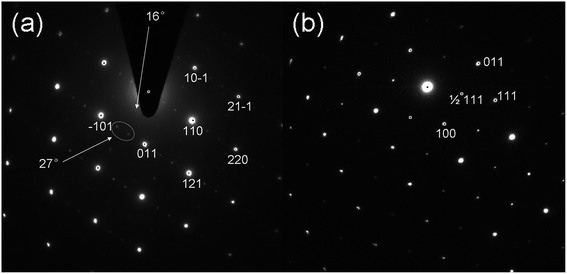 |
| | Fig. 3 Electron diffraction patterns of antiferroelectric phase obtained (a) in the [1−11] zone and (b) in the [01−1] zone. | |
3.3 Domain
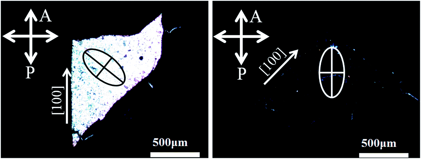
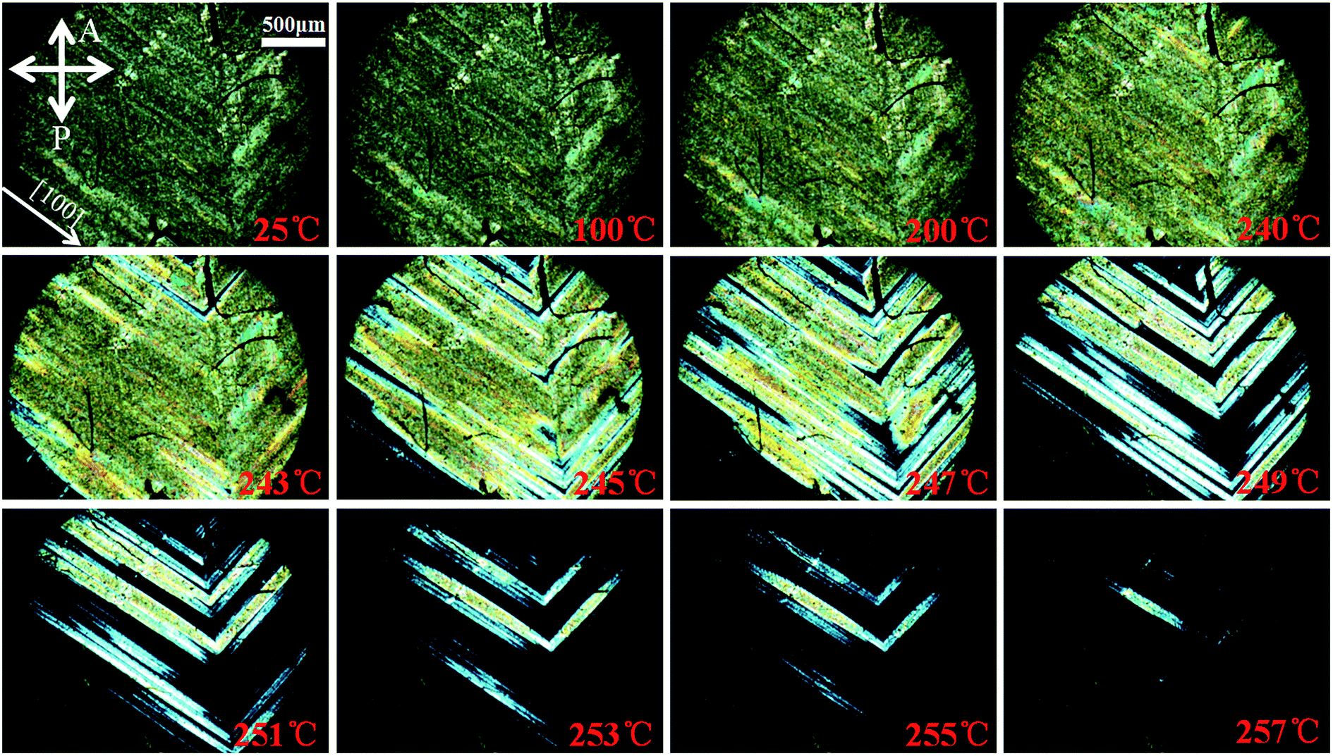
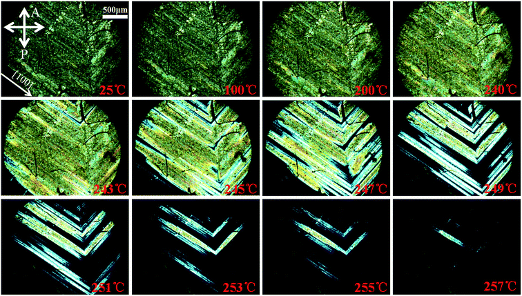
Antiferroelectric micro-domains configurations of PLN crystal were examined by TEM. Although low accelerating voltages and low ion currents were used to prevent the loss of PbO, the domain configurations can be easily modified,32 and the domain wall are expanded by the electron beam heating and the stability of the domains are changed. The change happens so fast that there is no time to take pictures. TEM study of the disorder–order perovskite Pb(Inl/2Nbl/2)O3 has shown that it is a relaxor ferroelectric in disordered PIN whereas an antiferroelectric behavior is observed in ordered PIN.33 In ordered PLN, an antiferroelectric micro-domains with 1–2 nm in size was also found, as shown in Fig. 4. In general, the spontaneous polarization (Ps) in the paraelectric perovskite cubic structure below TC appears in [110] directions in orthorhombic (O) perovskites. The vibration directions of all the domains in the (001) plate are practically parallel or perpendicular to each other and the extinction angle θ is defined as the smaller angle between the domain's vibration direction and the [100] crystallographic axis is practically the same for all domains.34 Viewed under crossed polarizers, the domains appear to be in extinction when their slow and fast vibration directions are along the vibration directions of polarizer (P) and analyzer (A), namely, θ = 45° or θ = 0° in the O phase.35 Fig. 5 shows the micrograph of the [001]-oriented plate of the PLN crystal under crossed polarizer at room temperature. The extinction of domains appear when θ = 45°, while the field manifests full bright when the objective table was rotated 45°, further confirming the orthorhombic symmetry of PLN crystal at room temperature. The domain structure and its extinction features in (001) PLN crystal plates as a function of temperature are shown in Fig. 6. The evolution of domain pattern was studied in the full bright field under crossed polarizers by heated from room temperature to 258 °C, where few change until 240 °C was observed. However, by continuous heating, some parts of the domains appear to be in extinction and the field slowly turns into all dark state at 258 °C, which demonstrates the phase transition from orthorhombic to cubic phase between 240–258 °C.
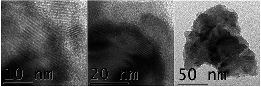 |
| | Fig. 4 Micro-domains configurations under TEM in the [1−11] zone. | |
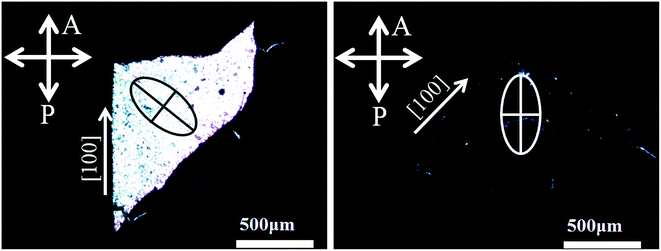 |
| | Fig. 5 Micrographs and its extinction angle of [001]-oriented plates of PLN crystal under crossed polarizer at room temperature. | |
 |
| | Fig. 6 Micrographs and its temperature dependence of [100]-oriented plates of PLN crystal under crossed polarizer. | |
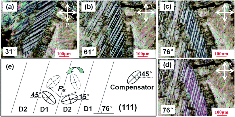
For [111]-oriented platelet of O phase, two or more domains with nonparallel vibration directions appear overlapped. The macro-domains are consisting of numerous micro-domains. Therefore, not all macro-domains show extinction simultaneously. It is found that the presence of macro-domains are about 10–20 μm in size within two sets of domains, as shown in Fig. 7. One set of the domains (D1) appears to be in extinction when the objective table is in the angle of 31° (the angle defined as the angle between polarizer and the strip of domain) but the other set of the domains (D2) appears to be in extinction when the objective table is in the angle of 61°, as shown in Fig. 7(a) and (b), respectively. When the angle is set as 76°, D1 manifests full bright, as shown in Fig. 7(c). In order to confirm the orientation of the spontaneous polarization, a 530 nm optical path compensator plate was inserted, the color of D1 remains first order white-grey (200–300 nm) but the color of D2 turns from first order black-grey to first order pink (500–550 nm), as shown in Fig. 7(d). Based on crystal optical principle,34 the Ps of the adjacent domains was confirmed as shown in Fig. 7(e). The domain walls form an angle of 120° within one of the (111) plate, which is 60° domain walls in space, namely.
 |
| | Fig. 7 Micrographs, domain size and domain wall angle of [111]-oriented plates PLN crystal under crossed polarizer at room temperature. | |
3.4 Phase transition
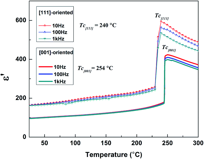
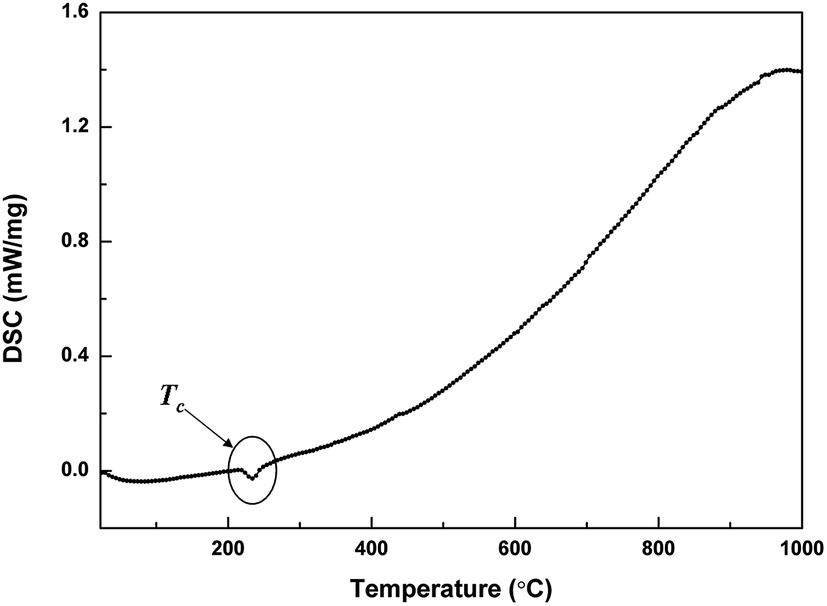
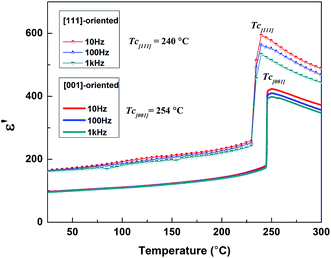
Fig. 8 shows the temperature dependence of the dielectric constant (ε′) at various frequencies for unpoled [111]-oriented and [001]-oriented PLN crystal plate. It shows a sharp peak at T = 240 °C and 254 °C for [111]-oriented and [001]-oriented crystal plates respectively, corresponding to the Tmax, which is the temperature of the maximum dielectric constant. Generally, the Tmax is related to the measurement frequency. So the value of Tmax at 1k Hz is considered to be Curie temperature TC habitually. No obvious frequency dispersion is found near Tmax, indicating the normal antiferroelectric behavior. The Curie temperature of PLN single crystals is lower than that of PLN ceramics which also undergoes a sharp antiferroelectric–paraelectric phase transition at about 258 °C without dielectric dispersion.10,14 The difference temperature is due the component differences between single crystals and ceramics. Like most antiferroelectric materials, the value of ε′ of PLN crystal (about 162, 90 for [111]-oriented and [001]-oriented crystal at room temperature respectively) is not very high. The difference of dielectric properties can be explained by the anisotropic behavior. It is known that the possible polarization directions for orthorhombic perovskite symmetry is along the [110] direction. The polarization rotation mechanism induced by external electric fields along certain paths is proposed to explain the high dielectric constant for [111]-oriented samples due to the easy rotation and incline of domain and polar vectors.36 In addition, the orthorhombic to cubic transition temperature was confirmed by the DSC curves of the PLN crystal, exhibiting at 234 °C as shown in Fig. 9, in agreement with the data obtained from dielectric data.
 |
| | Fig. 8 Temperature dependence of the dielectric constant (ε′) at various frequencies for unpoled [111]-oriented and [001]-oriented plates of PLN crystal. | |
 |
| | Fig. 9 Differential Scanning Calorimeter of the crashed PLN crystal sample. | |
3.5 Antiferroelectric properties
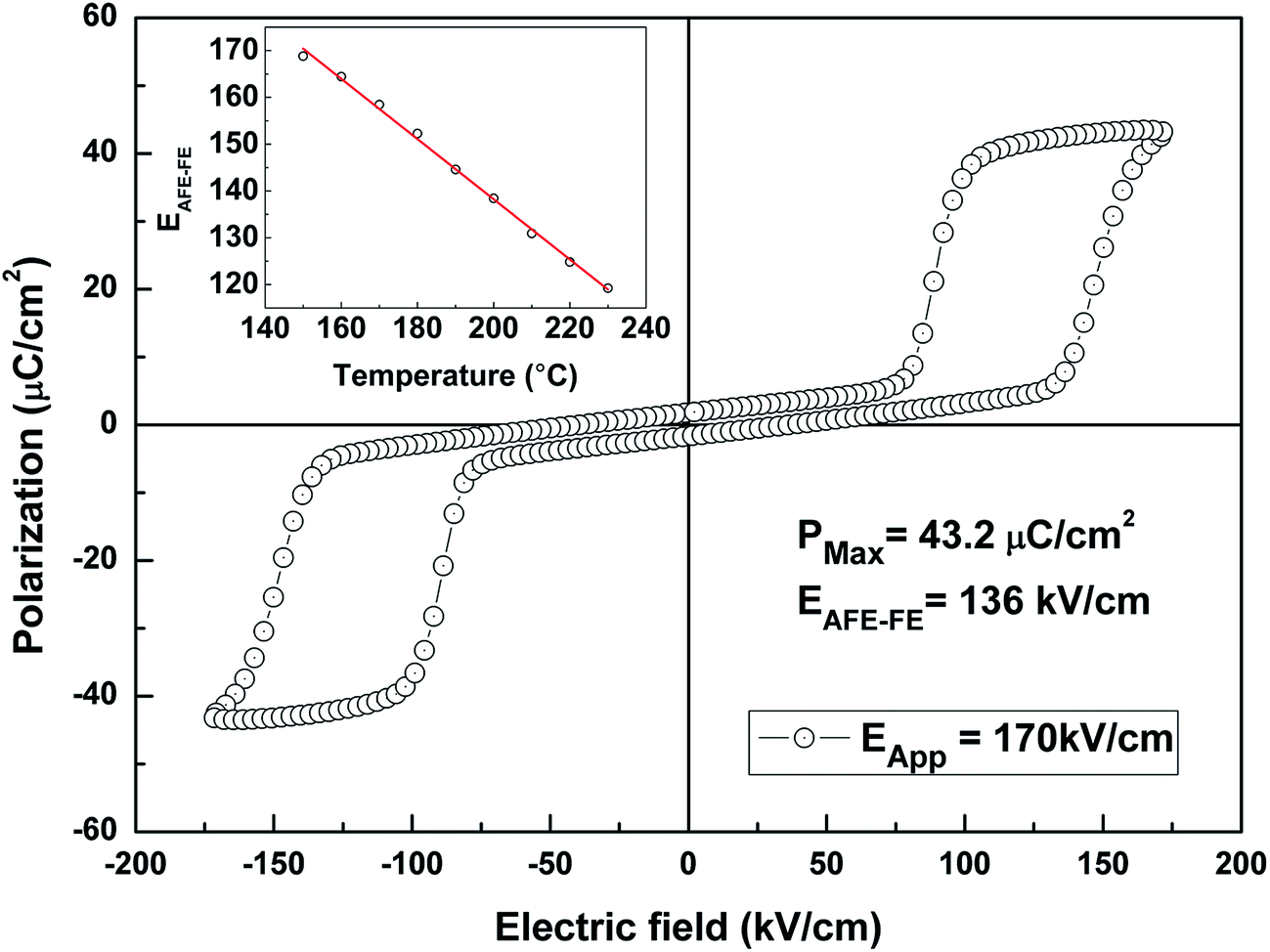
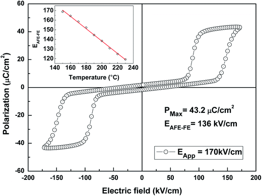
When high-occupancy order exists between the B-site cations, nanoscale chemical gradient appears with long-range normal antiferroelectric behavior.10 With an electric field EAPP = 170 kV cm−1 applied at room temperature (f = 10 Hz), the polarization–electric field (P–E) hysteresis loops of [111]-oriented PLN crystal platelets show that the P–E relationship is rather linear. It should be pointed out that it is difficult to obtained saturated double hysteresis loops at low temperature because the samples are easily broken down due to high AFE/FE transition electric field and low breakdown strength. In order to get the saturated double hysteresis loops, the AFE/FE hysteresis loops for PLN crystals were measured at high temperature which close to TC. Fig. 10 shows the polarization–electric field (P–E) hysteresis loops of [111]-oriented PLN crystal platelets with an electric field EAPP = 170 kV cm−1 (f = 10 Hz) applied at 200 °C. It can be seen that there is a double hysteresis loop with small remnant polarization (∼1 μC cm−2) and a high induced polarization (Pmax ∼ 43.2 μC cm−2) in the P–E curves. When electric field is increased larger than 136 kV cm−1, the antiferroelectric phase was transformed into a ferroelectric phase, namely, the antiferroelectric phase to ferroelectric phase transition field EAFE–FE = 136 kV cm−1. Whereas the electric field was reduced less than 75 kV cm−1, the metastable ferroelectric phase returned to antiferroelectric phase and macro-polarization disappeared. Large electric energy is stored and released in the transition process. The smallest value for an electric field that can prevent the transition from metastable ferroelectric phase into antiferroelectric phase is EFE–AFE = 75 kV cm−1. Antiferroelectric to ferroelectric transition leads to high energy storage for the DC field, because of the large increase in polarization that accompanies the transition. Energy storage capabilities are determined experimentally by simple electrical circuit theory.37 The value of energy density was calculated, which was approximately 3.65 J cm−3 at 200 °C with 170 kV cm−1 electric field applied. From the dependence of energy density on field strength and temperature, it can be predicted that the attained saturation energy density is higher at room temperature. Such materials show promise for energy storage applications. Compared with the energy density of PLN ceramics which is 1.95 J cm−3 measured at 200 °C with f = 50 Hz, PLN crystals has obvious advantages.17 Meanwhile, the temperature dependence of antiferroelectric parameter of EAFE–FE for PLN crystal below TC is also displayed in the inset of Fig. 10. It is obvious that the EAFE–FE shows a linear reduction as temperature increased from 140 °C to 230 °C, indicating coincidence antiferroelectric characterization: with the increasing temperature, the antiparallel dipole would be easily reversed under EAPP. Therefore, the EAFE–FE at room temperature can be extrapolated to be 250 kV cm−1, which is much higher than the breakdown field. Hence a double hysteresis loop at room temperature cannot be obtained.
 |
| | Fig. 10 Polarization vs. electric field (P–E) loops for the [111]-oriented plates PLN crystal at 200 °C (f = 10 Hz). Temperature dependence of antiferroelectric parameter of EAFE–FE for PLN crystal below TC (inset), showing an ideal linear relationship between temperature and EAFE–FE. | |
4. Conclusions
The antiferroelectric single crystals of PLN with a tetrakaidecahedron combination were successfully grown by high-temperature solution technique using PbO–H3BO3 flux. The crystal structure was found to be orthorhombic in nature, as revealed by the analysis of the XRD date. Both XRD and TEM show two sets of superlattice reflections originating respectively from the B-site atom ordering and the lead-atom antiparallel ordering. High degree of order of B-sites occupancy was demonstrated by the superlattice reflections and the chemical order of the as grown PLN crystals. An antiferroelectric micro-domains with 1–2 nm in size has been found on (111) surfaces of PLN single crystal using TEM. The macro-domains consisting of numerous micro-domains have also been found by PLM. The temperature dependence of domains, extinction angle and domain wall angle has been studied under PLM. The normal dielectric behavior is somewhat different from the previous reports in PLN ceramics. The Curie temperature TC was detected, to be near 240 °C. The polarization–electric field (P–E) hysteresis loops of PLN crystal platelets along [111]-oriented were displayed, with EAFE–FE = 136 kV cm−1 and EFE–AFE = 75 kV cm−1 under EAPP = 170 kV cm−1. The value of energy density was calculated, which was approximately 3.65 J cm−3 at 200 °C. It is suggested that the PLN single crystals can constitute a new resource of high Curie temperature, high energy storage capabilities antiferroelectric-crystals potentially useful for high energy density electrical capacitors especially for large size capacitor devices that require a wider operation temperature range.
Acknowledgements
This work was supported by the National Natural Science Foundation of China under Grant No. 91422303, 51602308, 11504373 and 11404331, the Strategic Priority Research Program of the Chinese Academy of Sciences, Grant No. XDB20000000, and the Science and Technology Project of Fujian Province under Grant No. 2015H0049.
References
- C. Kittel, Theory of antiferroelectric crystals, Phys. Rev., 1951, 82, 729–732 CrossRef CAS.
- G. Shirane, E. Sawaguchi and Y. Takagi, Dielectric properties of lead zirconate, Phys. Rev., 1951, 84, 476–481 CrossRef CAS.
- E. Sawaguchi, Ferroelectricity versus antiferroelectric in the solid solutions of PbZrO3 and PbTiO3, J. Phys. Soc. Jpn., 1953, 8, 615–629 CrossRef CAS.
- G. Shirane and K. Suzuki, Crystal structure of Pb(Zr,Ti)O3, J. Phys. Soc. Jpn., 1952, 8, 7333–7342 Search PubMed.
- Z. Xing, Y. J. Feng and X. Y. Wei, Effect of Sn content on dielectric, piezoelectric and ferroelectric properties for Pb(Zr0.35Ti0.65)1−xSnxO3 ceramics near morphotropic phase boundary, J. Alloys Compd., 2015, 627, 238–243 CrossRef CAS.
- L. Zhang, S. L. Jiang, B. Y. Fan and G. Z. Zhang, High energy storage performance in (Pb0.858Ba0.1La0.02Y0.008)(Zr0.65Sn0.3Ti0.05)O3–(Pb0.97La0.02)(Zr0.9Sn0.05Ti0.05)O3 anti-ferroelectric composite ceramics, Ceram. Int., 2015, 41, 1139–1144 CrossRef CAS.
- A. Pathak, R. Chatterjee and C. Prakash, Improvement in shape memory in magnesium niobate modified PZST, Ceram. Int., 2010, 36, 2263–2267 CrossRef CAS.
- W. Y. Pan, C. Q. Dam, Q. M. Zhang and L. E. Cross, Large displacement transducers based on electric field forded phase transitions in the tetragonal Pb0.97La0.02(Zr,Sn,Ti)O3 family of ceramics, J. Appl. Phys., 1989, 66, 6014–6023 CrossRef CAS.
- J. R. Kwon and W. K. Choo, The antiferroelectric crystal structure of the highly ordered complex perovskite Pb(Yb1/2Nb1/2)O3, J. Phys.: Condens. Matter, 1991, 3, 2147–2155 CrossRef CAS.
- Y. Park and K. Cho, Dielectric-state analysis in solid-solution Pb(Yb1/2Ta1/2)O3-Pb(Lu1/2Nb1/2)O3, J. Am. Ceram. Soc., 2000, 83, 135–140 CrossRef CAS.
- W. F. Wu, Y. Zhang, Q. Zhang, X. R. Wang and X. Z. Song, Characterization of PLZST-PMW dielectric ceramics, Mater. Res. Bull., 2014, 60, 183–187 CrossRef CAS.
- Q. H. Zhang, Y. Y. Zhang, F. F. Wang, D. Lin, X. B. Li, X. Y. Zhao and H. S. Luo, Growth and electric properties of 0.96Na0.5Bi0.5TiO3–0.04BaTiO3 single crystal, J. Cryst. Growth, 2010, 312, 457–460 CrossRef CAS.
- E. M. Alkoy and M. Papila, Microstructural features and electrical properties of copper oxide added potassium sodium niobate ceramics, Ceram. Int., 1921, 36, 1921–1927 CrossRef.
- A. Sternberg, L. Shebanovs, E. Birks, Y. Yamashita, M. Tyunina and V. Zauls, Effects of structure ordering, structure defects and external conditions on properties of complex ferroelectric perovskites, Ferroelectrics, 1998, 217, 307–317 CrossRef CAS.
- A. Stemberg, L. Shebanovs, M. Antonova, M. Livinsh, J. Y. Yamashita, L. Shombalko and A. Spule, New high piezoelectric coupling PLuNT binary system ceramics, Nanostruct. Mater., 1999, 12, 645–648 CrossRef.
- A. Sternberg, L. Shebanovs, V. Zauls, K. Kundzins, M. Antonova, M. Livins, L. Cakare, M. Tyunina, J. Levoska and I. Aulika, Structure and properties of Pb(LuNb)O3–PbTiO3 ceramics and thin films, Ferroelectrics, 2003, 294, 41–47 CAS.
- X. M. Yang, Y. Liu, C. He, H. Tailor and X. F. Long, La-modified Pb(Lu1/2Nb1/2)O3 antiferroelectric ceramics with high energy storage density, J. Eur. Ceram. Soc., 2015, 35, 4173–4180 CrossRef CAS.
- L. Zhang, S. L. Jiang, Y. K. Zeng, M. Fu, K. Han, Q. Li, Q. Wang and G. Z. Zhang, Y doping and grain size co-effects on the electrical energy storage performance of (Pb0.87Ba0.1La0.02)(Zr0.65Sn0.3Ti0.05)O3 anti-ferroelectric ceramics, Ceram. Int., 2014, 40, 5455–5460 CrossRef CAS.
- S. E. Young, J. Y. Zhang, W. Hong and X. Tan, Mechanical self-confinement to enhance energy storage density of antiferroelectric capacitors, J. Appl. Phys., 2013, 113, 054101 CrossRef.
- F. Zhuo, Q. Li, J. Gao, Y. Wang, Q. Yan, Y. Zhang, X. Xi, X. Chu and W. Cao, Coexistence of multiple positive and negative electrocaloric responses in (Pb,La)(Zr,Sn,Ti)O3 single crystal, Appl. Phys. Lett., 2016, 108, 082904 CrossRef.
- J. Gao, Q. Li, Y. Li, F. Zhuo, Q. Yan, W. Cao, X. Xi, Y. Zhang and X. Chu, Electric field induced phase transition and domain structure evolution in (Pb,La)(Zr,Sn,Ti)O3 single crystal, Appl. Phys. Lett., 2015, 107, 072909 CrossRef.
- Y. Li, W. Cao, Q. Li, Q. Yan, J. Gao, F. Zhuo, X. Xi, Y. Zhang and X. Chu, Electric field induced metastable ferroelectric phase and its behavior in (Pb,La)(Zr,Sn,Ti)O3 antiferroelectric single crystal near morphotropic phase boundary, Appl. Phys. Lett., 2014, 104, 052912 CrossRef.
- X. M. Yang, C. He, Y. Liu, X. Z. Li, Z. J. Wang, S. J. Han, S. L. Pan and X. F. Long, Antiferroelectric single crystal of La0.011Pb0.984(Lu1/2Nb1/2)O3 with high energy storage density, Ceram. Int., 2016, 42, 10472–10475 CrossRef CAS.
- M. Dong and Z.-G. Ye, High-temperature solution growth and characterization of the piezo-/ferroelectric (1 − x)Pb(Mg1/3Nb2/3)O3–xPbTiO3 [PMNT] single crystals, J. Cryst. Growth, 2000, 209, 81–90 CrossRef CAS.
- C. He, X. Z. Li, Z. J. Wang, X. F. Long, S. Y. Mao and Z.-G. Ye, Preparation and characterization of new Pb(Yb1/2Nb1/2)O3–Pb(Mg1/3Nb2/3)O3–PbTiO3 ternary piezo-/ferroelectric crystals, Chem. Mater., 2010, 22, 5588–5592 CrossRef CAS.
- X. X. Yan, D. L. Xu and D. F. Xue, SO42− ions direct the one-dimensional growth of 5Mg(OH)2·MgSO4·2H2O, Acta Mater., 2007, 55, 5747–5757 CrossRef CAS.
- D. L. Xu and D. F. Xue, Chemical bond analysis of the crystal growth of KDP and ADP, J. Cryst. Growth, 2006, 286, 108–113 CrossRef CAS.
- A. F. Devoshire, Theory of barium titanate -part I, Philos. Mag., 1949, 40, 1040–1055 CrossRef.
- M. A. Akbas and P. K. Davies, Cation ordering transformations in the Ba(Zn1/3Nb2/3)O3–La(Zn2/3Nb1/3)O3 system, J. Am. Ceram. Soc., 1998, 81, 1061–1064 CrossRef CAS.
- Z. G. Xia and Q. Li, Phase transformation in (0.90 − x)Pb(Mg1/3Nb2/3)O3–xPbTiO3–0.10PbZrO3 piezoelectric ceramic: X-ray diffraction and Raman investigation, Solid State Commun., 2007, 142, 323–328 CrossRef CAS.
- H. Fuiishita, Y. Shiozaki, N. Achiwa and E. Sawaeuchi, Crystal structure determination of antiferroelectric PbZrO3: application of profile analysis method to powder method of X-ray and neutron diffraction, J. Phys. Soc. Jpn., 1982, 51, 3583–3591 CrossRef.
- C. A. Randall and D. J. Barber, Ferroelectric domain configurations in a Modified-PZT ceramic, J. Mater. Sci., 1987, 22, 925–931 CrossRef CAS.
- C. A. Randall, D. J. Barber, P. Groves and R. W. Whatmore, TEM study of the disorder-order perovskite Pb(Inl/2Nbl/2)O3, J. Mater. Sci., 1988, 23, 3678–3682 CrossRef CAS.
- A. A. Bokov, X. F. Long and Z.-G. Ye, Optically isotropic and monoclinic ferroelectric phases in PZT single crystals near morphotropic phase boundary, Phys. Rev. B: Condens. Matter Mater. Phys., 2010, 81, 1248 CrossRef.
- Z. G. Ye, M. Dong and L. Zhang, Morphotropic domain structures and phase transitions of the relaxor-based piezo-/ferroelectric (1 − x)Pb(Zn1/3Nb2/3)O3–xPbTiO3 single crystals, J. Appl. Phys., 2000, 87, 2312–2319 CrossRef CAS.
- S. E. Park and T. R. Shrout, Ultrahigh strain and piezoelectric behavior in relaxor based ferroelectric single crystals, J. Appl. Phys., 1997, 82, 1804–1811 CrossRef CAS.
- K. Singh, Antiferroelectric lead zirconate, a material for energy storage, Ferroelectrics, 1989, 94, 433 CrossRef.
|
| This journal is © The Royal Society of Chemistry 2017 |
Click here to see how this site uses Cookies. View our privacy policy here. 
 Open Access Article
 This Open Access Article is licensed under a
  *a
*a