
 Open Access Article
 This Open Access Article is licensed under a
 Creative Commons Attribution 3.0 Unported Licence
Probing the nano-scale architecture of diamond-patterned electrospun fibre mats by synchrotron small angle X-ray scattering
Tan Sui a,
Kirill Titovb,
Siqi Yinga,
Hongjia Zhanga,
Igor P. Dolbnyac,
Jin-Chong Tanb and
Alexander M. Korsunsky*a
a,
Kirill Titovb,
Siqi Yinga,
Hongjia Zhanga,
Igor P. Dolbnyac,
Jin-Chong Tanb and
Alexander M. Korsunsky*a
aMBLEM, Department of Engineering Science, University of Oxford, Parks Road, Oxford OX1 3PJ, UK. E-mail: alexander.korsunsky@eng.ox.ac.uk
bMMC, Department of Engineering Science, University of Oxford, Parks Road, Oxford, OX1 3PJ, UK
cBeamline B16, Diamond Light Source, Harwell Campus, Didcot OX11 0DE, UK
First published on 23rd January 2017
Abstract
A diamond-patterned polyvinylpyrrolidone (PVP) fibre mat manufactured by electrospinning onto a structured target was studied by the combination of electron microscopy and synchrotron small angle X-ray scattering. Multi-scale hierarchical structure analysis revealed the relationship between different morphological levels, from an overall mat layout to individual fibres to polymer fibril orientation within them.
Electrospinning is a remarkably versatile technique for the production of fine fibres with diameters in the range from microns to tens of nanometres and unique properties that make them attractive for a wide range of practical applications, e.g. in energy storage, gas capture, filtration, optoelectronics and sensors, drug delivery and medicine.1,2 Electrospinning produces fibres by pulling a fine jet of a polymer solution from a Taylor cone, which then undergoes a bending and whipping instability, solidifying in the process. This jet is highly sensitive to the applied electric field. Therefore, controlled deposition of fibres onto the target electrode can be achieved by selecting a suitable target structure, e.g. a single slot, mesh, etc. Structured conductive collecting substrates such as wire grids have been used to produce nano-fibrous mats that are patterned according to the underlying electric field. Patterned fibre mat structures can be deposited in the form of doubly periodic repetition of “unit cells”. Mats with varying fibre distributions and arrangements may potentially be constructed in the course of a single electrospinning run using a substrate with differently patterned surface tailored for specific applications. Patterned nanofibre mats have attracted growing interest due to their remarkable mechanical properties3,4 and versatility, making them promising candidates for biomedical applications5 compared with un-patterned nanofibre mats. To be able to exploit better the mechanical and functional properties of patterned electrospun fibre mats, the investigation of multi-scale structural features from the micro- to nano-meter scale is crucial.
A variety of experimental techniques have been employed to characterise the internal structure of electrospun fibres, such as atomic force microscopy (AFM),6 polarized infrared spectroscopy (IR)7 and diffraction based techniques of wide angle X-ray diffraction and small angle X-ray scattering (SAXS).2 Among these techniques, synchrotron-based SAXS is one of the most versatile non-destructive techniques capable of acquiring quantitative structural information at the nano-scale, and allowing to explore the fibril distribution within individual fibres.2,8 Despite the research effort invested in the study of electrospun fibres so far, very limited exploration and understanding of the hierarchical architecture of patterned electrospun fibre mats has been achieved.
In this work, we report the use of electron microscopy and synchrotron small angle X-ray scattering (SAXS) measurements for the characterisation of the micro- and nano-structure of diamond-patterned electrospun fibre mats. We seek to achieve further understanding of the correlation between the fabricated structure and its properties, to help guide, control and optimise the processing parameters, such as the electric field strength, collector shape and polymer solution. This will ultimately allow using feedback from the structure and performance assessment to develop robust reliability-based design and optimisation for customised products.
Polyvinylpyrrolidone (PVP) powder with the average molecular weight of Mw ∼1![[thin space (1/6-em)]](https://www.rsc.org/images/entities/char_2009.gif) 300000 was dissolved in methanol (MeOH; both acquired from Sigma-Aldrich) to produce the electrospinning polymer solution. In the preliminary experiments, continuous fibres with good surface quality and diameters ranging from 2 to 4 μm (depending on the processing parameters used) were successfully produced by electrospinning from polymer solutions with 20 wt% of PVP in MeOH. The resulting mats consisted of randomly oriented fibres that were fully amorphous, as confirmed by X-ray scattering. In the in situ experiment described in the present report, polymer solution was supplied to the G19 needle emitter (nozzle) with a blunt tip via a syringe pump at a flow rate of 2 mL h−1. The needle was positioned vertically over the diamond-shaped Cu mesh collector, with the needle-to-collector distance of 15 cm, and applied voltage of 10 kV, depending on the solution concentration and flow rate. A nominal thickness of ∼200–300 μm of each mat was generated, without the patterned architecture of highly ordered fibrous mats in the diamond shape preserved throughout the process.
300000 was dissolved in methanol (MeOH; both acquired from Sigma-Aldrich) to produce the electrospinning polymer solution. In the preliminary experiments, continuous fibres with good surface quality and diameters ranging from 2 to 4 μm (depending on the processing parameters used) were successfully produced by electrospinning from polymer solutions with 20 wt% of PVP in MeOH. The resulting mats consisted of randomly oriented fibres that were fully amorphous, as confirmed by X-ray scattering. In the in situ experiment described in the present report, polymer solution was supplied to the G19 needle emitter (nozzle) with a blunt tip via a syringe pump at a flow rate of 2 mL h−1. The needle was positioned vertically over the diamond-shaped Cu mesh collector, with the needle-to-collector distance of 15 cm, and applied voltage of 10 kV, depending on the solution concentration and flow rate. A nominal thickness of ∼200–300 μm of each mat was generated, without the patterned architecture of highly ordered fibrous mats in the diamond shape preserved throughout the process.
The acquisition of 2D maps of the electrospun mat using Small-Angle X-ray Scattering (SAXS) was carried out at the synchrotron X-ray bending magnet Test Beamline B16 at Diamond Light Source, UK. Multilayer Monochromator (MLM) (Ru/B4C: 8 keV) was used to ensure X-ray high flux delivery by efficient scattering of the monochromatic beam. The beam was collimated to the 200 × 200 μm spot size. The sCMOS “X-ray Eye” transmission imaging detector (Photonic Science Ltd., UK) was first placed in the uncollimated transmitted beam to obtain radiographic images and identify the region of interest (ROI) on the sample. This imaging detector was then translated laterally out of the beam path to allow the sample scattering pattern to be captured by the SAXS detector (Pilatus 300K detector, Dectris, Baden, Switzerland). 2D mapping was performed on the ROI by rastering the sample across the collimated beam in the horizontal and vertical directions with the steps of 200 μm in both x- and y- directions. For the purpose of precise determination of the sample-to-detector distance (4184 mm) and of the centre of scattering pattern on the detector, a disk of silver behenate (AgBe) powder was put at the sample position, and the concentric ring pattern collected from it was used for SAXS calibration.9
SAXS patterns provide a wealth of information related to the nanostructure of the scattering object. Scattering contrast arises from the variation of electron density within the sample, meaning that SAXS pattern formation is related to the presence of interfaces and gradients of electron density within the sample.8 The angular coverage provided by the detector determines the range of dimensions in real space that contribute to the observed scattering patterns. In the configuration used in this study the length scales covered by the setup were in the range ∼10–100 nm. This meant that the information obtained from SAXS data interpretation was complementary to that collected using conventional real space examination tools, such as SEM, which allow visualisation of the exterior shape (morphology) of electrospun fibres down to length scales of fractions of a micron.
Quantitative interpretation of SAXS patterns allows the determination of the mean transverse dimension T of the scattering features, a conventional parameter used to describe average scattering object size, and preferred orientation.10 The mean dimension of the scattering object can be determined in two steps: firstly, the scattering intensity is integrated over the entire range of azimuthal angle, leading to a 1D function Î(q) that depends on q, the scattering vector length (Fig. 1). The Porod constant P and the background level B are obtained from the so-called Porod plot of Î(q) × q4 vs. q4. Secondly, based on the integral area Q under the curve of Î(q) × q2 vs. q. From these two instances of analysis, the mean dimension T, also known as the Porod chord length that represents the total surface area of scattering objects per unit volume, is determined as T = (4/π) × (Q/P).
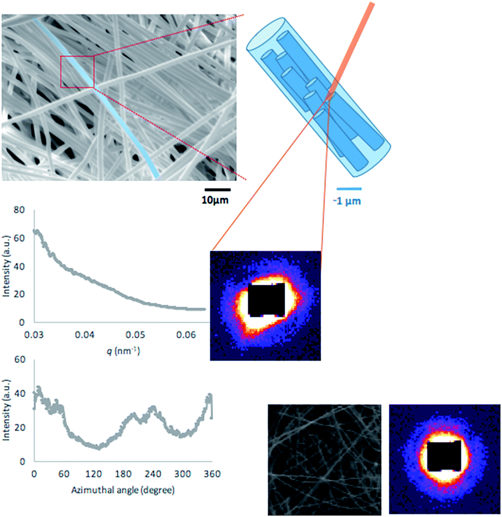 | ||
| Fig. 1 SAXS data interpretation of a representative 2D scattering pattern arising from the arrangement of fibres convoluted with the distribution of fibrils within individual fibres. This can be converted to 1D profiles by azimuthal (upper) and radial (lower) integration. | ||
Further, the preferred orientation and the degree of alignment of the scattering objects can also be determined by the following two steps. Firstly, the scattering intensity I(q, φ) is integrated over the entire range of the scattering vector q at each azimuthal angle φ to obtain the function Î(φ) (Fig. 1). The preferred orientation is then defined as the position (or azimuthal angle) of the peak intensity in Î(φ) ± 90° (where ± is used to ensure that the preferred orientation lies between 0 and 180°). The degree of alignment is defined as the height of the peak above the lowest value, divided by that value. For comparison, the inset at the bottom right of Fig. 1 (full frame width corresponding to 200 μm) shows the structure of the electrospun mat obtained using a flat unpatterned target, along with the corresponding SAXS scattering pattern.
As a consequence of electrospinning deposition of fibres onto the diamond-shaped mesh, the produced non-woven sheet of micro-scale fibres mimics the architecture of the mesh collector. The macroscopic image is shown in Fig. 2(a), where a highly ordered fibrous matrix can be clearly observed. The corresponding map of X-ray scattering integrated intensity is shown in Fig. 2(b). It can be seen that the X-ray scattering intensity map reflects the shape of individual unit cells and the periodical structure of the diamond. Stronger scattering intensity is observed within the ‘walls’ (above 6000 a.u.) compared to the ‘cells’ (below 5000 a.u.). Since the intensity increases with the concentration of fibres, this indicates the increased density of fibres deposited within the walls compared to the cells. In addition, Fig. 2(b) also reveals the variation of the scattering intensity between different unit cells, and even local intensity singularities in several cell walls (in excess of 10000 a.u.). Since electrospinning fibre deposition has been shown to be sensitive to small differences in the electric field profile,1 this non-uniform scattering intensity can be correlated with a number of factors that affect the deposition, including non-uniform in-plane electric field intensity and uneven surface of the conductive mesh collector.
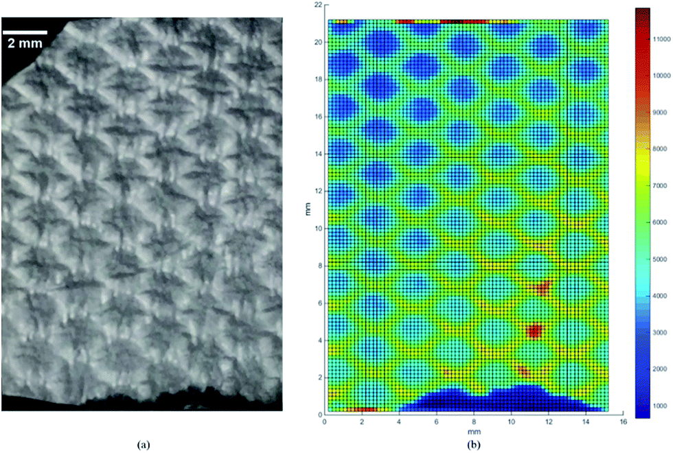 | ||
| Fig. 2 Diamond-patterned electrospun fibrous mat. (a) Optical image of the PVP fibrous mat; (b) map of the integrated intensity of X-ray small angle scattering obtained from 2D mapping of the same region of the mat. | ||
Closer inspection of a diamond-shaped unit cell by SEM (Carl Zeiss EVO LS15 SEM) shown in Fig. 3(a) illustrates the microstructure and arrangement of micro-scale fibres. SEM imaging reveals the ordered structure of this diamond-patterned electrospun fibre mat with approximately uniform wall width. The sketch of the unit cell dimension is shown in Fig. 3(b), with the two diamond-cell dimensions of 2.8 mm (horizontal) and 1.7 mm (vertical), respectively, while the average width of the walls is ∼500 μm. It is also apparent that the fibre density is considerably higher in the walls of the PVP structured fibrous mat compared to the cell interior. Nevertheless, fibres are clearly present within cell interiors that provide bridging connections between walls. The fibres making up the walls appear to be preferentially aligned along the sides of the diamond pattern (Fig. 3(a)). In contrast, cell interiors are occupied with approximately randomly oriented fibres. Since the electric field is not strongly directional within the unit cell interior, the fibre alignment and deposition density variation provide a link between the geometry of the mat, through the non-uniform and directional electric field, to the structure of the electrospun mat. The electrospinning jet is attracted to the charged ‘struts’ of the wire mesh, whilst the presence of neighbouring struts creates the possibility of diverting the spinning fibres to adjacent cells. Overall, this results in distinct regions of high fibre density in the walls and low fibre density in the cell interiors.11 Statistical analysis of the fibre dimensions show the fibres located within the wall appear to be significantly thinner (∼2 μm) compared to those lying within the cells (diameter ∼3 μm). This has been attributed to the greater stretching force acting on the fibres when they are attracted to the mesh struts underlying the walls, where the local inhomogeneity of the electric field create greater gradients of potential.1,12
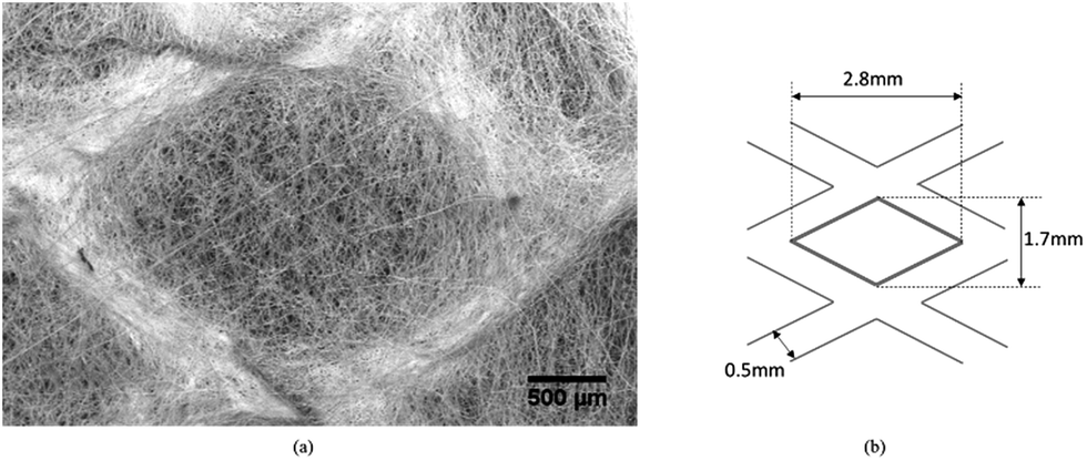 | ||
| Fig. 3 The morphology of a diamond-shaped unit cell imaged at the micro-scale. (a) SEM observation of a single unit cell; (b) sketch of the unit cell dimensions. | ||
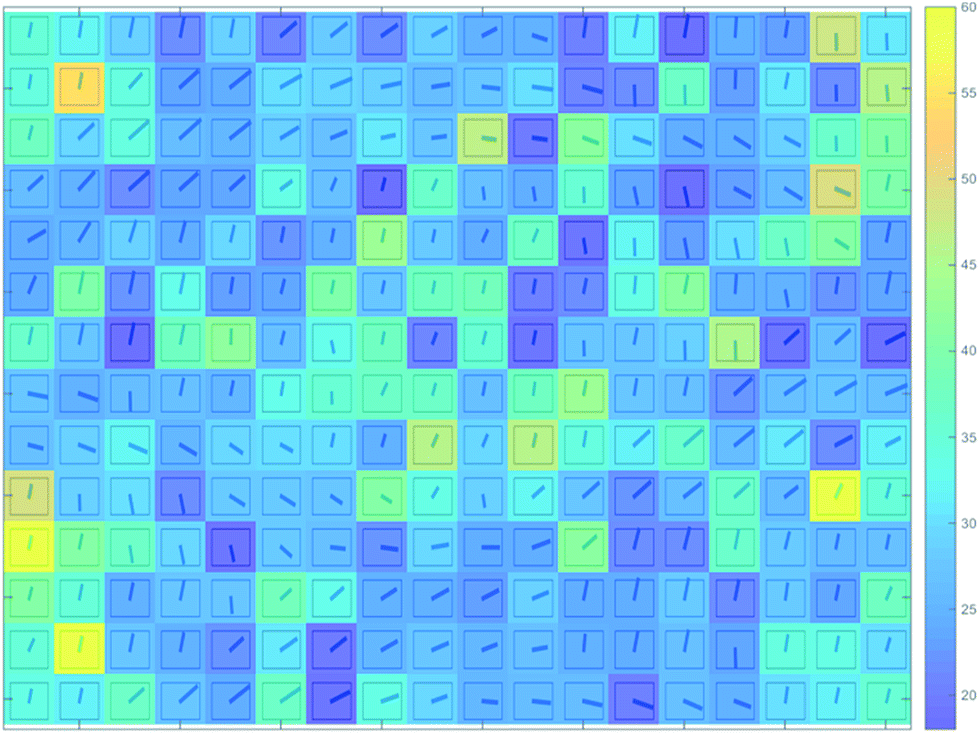
A single unit cell was selected for X-ray scanning examination. In total, Small Angle X-ray Scattering (SAXS) patterns were recorded at 18 × 14 scanning positions, as shown in Fig. 4.
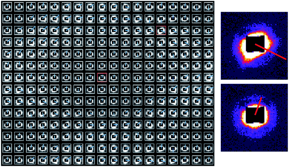 | ||
| Fig. 4 Orientation distribution of fibrils within a unit cell revealed by SAXS raster scan at 18 × 14 positions. A blue bar on each scanned image indicates the preferred orientation (bar direction) and the degree of alignment (bar length) of fibrils at each position. Two representative patterns, one from the unit cell ‘wall’ (upper) and one from the cell interior (lower) are shown on the right. | ||
SAXS is sensitive to the nano-scale internal structure of polymer, since scattering contrast is formed due to the interaction of X-ray wavefront with electron density gradients associated with the bundles of polymer molecules, or fibrils, contained within individual fibres.2 SAXS patterns were interpreted to extract the relevant ultrastructural information in the form of 2D maps. The interpretation of SAXS patterns in terms of the preferred orientation and degree of alignment as described in the previous section devoted to methods allows a correlation to be established between the exterior and interior structure of the mat, i.e. revealing how the arrangement of fibrils within individual fibres is related to their lay-up within the mat. Fig. 4 shows the SAXS patterns from each scanning position with a blue bar superimposed on each pattern. The direction of the blue bars represents the preferred orientation extracted from SAXS analysis, while the length of the bar corresponds to the degree of alignment of the internal fibrils within the fibres.
The black square that appears at the centre of each SAXS patterns represents the beam stop. Brightness of each image corresponds to the scattering intensity which increases with the number of fibrils that contribute to the scattering. It is worth noting that ‘spikes’ appear in some patterns, disrupting the elliptical or circular SAXS pattern structure. This indicates deviation from homogeneity within the underlying structure.
In general, it is observed that as a rule, elliptical patterns largely occur along the wall positions of the unit cell, whilst approximately circular scattering patterns occur in the cell interior. The orientation distribution of the blue bars is clearly analogous to that of the micro-fibres observed at the micro-scale by SEM (Fig. 3(a)). Within the walls, the direction of the bars aligns with the edge of the diamond shape, and the bars are clearly longer at these positions compared with those within the cells. Overall, this provides overwhelming evidence that the alignment of fibrils at the nano-scale coincides with that of the fibres themselves at the micro-scale within the cell walls (Fig. 3(a)). The degree of fibril alignment in these regions is clearly greater than that of fibres in the gaps. In addition, it can be noted that despite the reduced degree of orientation within the cells (indicated by the shorter bar lengths), fibrils still display systematic alignment that is mostly vertical. This observation is likely to be linked with the non-uniform nature of the in-plane electric field within the diamond-shaped mesh. The shorter unit cell dimension of the mat in the vertical direction is likely to lead to the electric field component is likely to be stronger compared to the horizontal direction, causing the fibres to be deposited with preferred axis orientation in the vertical direction.1
In order to take the data interpretation further, 2D contour plot of the mean fibril dimension collected from each scanning position in the unit cell was compiled based on the calculation of scattering object dimensions from the SAXS patterns. The resulting map is illustrated in Fig. 5, with the colour bar indicating the Porod transverse chord length (approximately corresponding to the average fibril diameter) in the units of nm. To explore the correlation between morphology, orientation and mean dimension, the map is superimposed with the orientation for each pattern, indicated by the blue bar. Whilst significant fluctuation of cross-sectional fibril dimension is observed within the cell interiors, in the walls the values of this parameter appear to be more uniform, and the map colour is continuous. There is no evident correlation to be seen between the fibril dimensions and orientation distribution, in the sense that the mean fibril dimension (cross-sectional diameter) appears to be independent from the position of the scattering volume within the unit cell. This suggests that the fibril structure remains rather stable and persistent at the nano-scale, in spite of the significant differences that can be observed at the micro-scale level via real space imaging of the fibre distribution within cells and in the walls (Fig. 3).
 | ||
| Fig. 5 Mean fibril dimension of fibrils within a single unit cell. Mean fibril dimension was calculated at 18 × 14 positions on the unit cell. For illustration, the orientation distribution indicated by blue bars is superimposed at the location of each scanned image within the map. The colour bar shown on the right indicates the predominant lateral dimension of the scattering objects (average fibril cross-section diameters) in nm. | ||
Conclusions
In summary, the patterned nano-fibrous mat was produced by using a conductive structured collecting substrate that had a pattern consisting of repeated diamond-shaped unit cells composed of wire struts, forming a grid that created a non-uniform electric field at the collector. The characterisation of the multi-scale hierarchical architecture of the non-woven fibre mat was probed by employing different modalities progressively, from macroscopic morphology to SEM imaging at the micro-scale to reveal the fibre arrangement within a unit cell, to nano-scale ultrastructural fibril distribution within the electrospun fibres, using Small Angle X-ray Scattering (SAXS). Higher X-ray scattering intensity in the cell walls was evident compared to the cell interior, and can be linked to the higher concentration and alignment of fibres within in the walls as the consequence of the high electric field gradient caused by the geometry of the wire struts in the mesh collector. The fibril distribution within a single unit cell of the electrospun mat revealed by SAXS resembles the SEM profile of fibre distribution perceived at the next larger structural scale, both in terms of the preferred orientation and degree of alignment of fibrils and fibres. It is concluded that a guided distribution of fibrils and fibres can be obtained using this fabrication approach, and that its further understanding and control are essential for further elucidation of the correlation between the function and structure of diamond patterned electrospun fibre mats. The results also shed light on the understanding of the mechanical properties, as well as the functionality and higher performance of these systems for future applications.Acknowledgements
Funding for the MBLEM laboratory at Oxford received under EU FP7 project iSTRESS (604646) is acknowledged, along with the access to the facilities at the Research Complex at Harwell (RCaH), under the Centre for In situ Processing Studies (CIPS).Notes and references
- K. Titov and J. C. Tan, APL Mater., 2016, 4, 086107 Search PubMed.
- M. Gazzano, C. Gualandi, A. Zucchelli, T. Sui, A. M. Korsunsky, C. Reinhard and M. L. Focarete, Polymer, 2015, 63, 154–163 CrossRef CAS.
- P. Gibson and H. Schreuder-Gibson, INJ Summer, 2014, 37, 34–41 Search PubMed.
- Y. Wang, G. Wang, L. Chen, H. Li, T. Yin, B. Wang, J. C. M. Lee and Q. Yu, Biofabrication, 2009, 1, 015001 CrossRef PubMed.
- N. M. Neves, R. Campos, A. Pedro, J. Cunha, F. Macedo and R. L. Reis, Int. J. Nanomed., 2007, 2, 433–438 CAS.
- C. T. Lim, E. P. S. Tan and S. Y. Ng, Appl. Phys. Lett., 2008, 92, 141908 CrossRef.
- M. V. Kakade, S. Givens, K. Gardner, K. H. Lee, D. B. Chase and J. F. Rabolt, J. Am. Chem. Soc., 2007, 127, 2777–2782 CrossRef PubMed.
- T. Sui, N. Baimpas, I. P. Dolbnya, C. Prisacariu and A. M. Korsunsky, Nat. Commun., 2015, 6, 6583 CrossRef PubMed.
- T. C. Huang, H. Toraya, T. N. Blanton and Y. Wu, J. Appl. Crystallogr., 1993, 26, 180–184 CrossRef CAS.
- T. Sui, M. A. Sandholzer, E. Le Bourhis, N. Baimpas, G. Landini and A. M. Korsunsky, J. Mech. Behav. Biomed. Mater., 2014, 32, 113–124 CrossRef PubMed.
- I. Ortega, A. J. Ryan, P. Deshpande, S. MacNeil and F. Claeyssens, Acta Biomater., 2013, 9, 5511–5520 CrossRef CAS PubMed.
- C. Vaquette and J. J. Cooper-White, Acta Biomater., 2011, 7, 2544–2557 CrossRef CAS PubMed.
| This journal is © The Royal Society of Chemistry 2017 |