
 Open Access Article
 This Open Access Article is licensed under a Creative Commons Attribution-Non Commercial 3.0 Unported Licence
The development of sol–gel derived TiO2 thin films and corresponding memristor architectures†
Valentina Prusakova*a,
Cristian Collinib,
Marco Nardiaf,
Roberta Tattif,
Lorenzo Lunellic,
Lia Vanzettie,
Leandro Lorenzellib,
Giacomo Baldig,
Andrea Chiappinid,
Alessandro Chiaserad,
Davor Ristichi,
Roberto Verucchif,
Mauro Bortolottia and
Sandra Dirèa
aDepartment of Industrial Engineering, University of Trento, Via Sommarive 9, 38123 Trento, Italy. E-mail: valentina.prusakova@unitn.it
bFBK, CMM – MICROSYSTEMS, Via Sommarive 18, 38123 Trento, Italy
cFBK, LABSSAH, Via Sommarive 18, 38123 Trento, Italy
dCNR-IFN, CSMFO Lab., Via Alla Cascata 56/C, 38123 Trento, Italy
eFBK, CMM – MNF, Via Sommarive 18, 38123 Trento, Italy
fCNR-IMEM, Via Alla Cascata 56/C, 38123 Trento, Italy
gDepartment of Physics, University of Trento, Via Sommarive 14, 38123 Trento, Italy
hDivision of Materials Physics, Laboratory for Molecular Physics, Ruđer Bošković Institute, Bijenička c. 54, Zagreb, Croatia
iResearch Unit New Functional Materials, Center of Excellence for Advanced Materials and Sensing Devices, Bijenička c. 54, Zagreb, Croatia
First published on 9th January 2017
Abstract
We report the development of sol–gel derived TiO2 thin films with adjustable and defined properties suitable for memristive cell fabrication. Memristive cells were developed by the sol–gel deposition of titania onto SiO2/Ti/Pt engineered electrodes via spin coating, followed by diverse curing and annealing procedures. The influence of the processing conditions and the sol's chemical composition on the film properties, and therefore on the memristive response, was studied by micro-Raman and transmission spectroscopies, profilometry, ellipsometry, X-ray photoelectron spectroscopy (XPS), atomic force microscopy (AFM), and X-ray absorption and diffraction spectroscopies (XAS and XRD). A memristive response was acquired from a number of these cells, revealing a dependence of the electrical behavior on minor changes in the TiO2 structure, electroforming parameters, and architecture. Thus, these properties provide a handle for fine-tuning electrical performance.
1. Introduction
Modern demands on computer performance require improvements in power consumption, speed, and both microprocessor and memory scalability.1 One of the most promising emerging technologies is a memristor-based RRAM memory with a plain cross-bar structure that ensures higher density than other memory technologies.2–4 Moreover, the memristor simultaneously supports logic and memory,5,6 fulfilling the conditions for the fourth fundamental circuit element in neuromorphic computation.7 One of the most studied memristive systems is a TiO2 thin film sandwiched between two electrodes.4 Despite numerous reports discussing the microscopic origin of the switch mechanism in TiO2,8–12 questions remain about the influence of material features on the memristive response, such as crystallinity, nanostructure, stoichiometry, and defects. Here, we highlight theoretical considerations for the desired material properties of a switchable resistive layer and describe the dependence of the memristive response on TiO2 features, electroforming parameters, and architecture of the device. The impact of the sol composition and processing parameters on the material properties and, therefore, on the memristive response was investigated. Additionally, the interface with the electrodes and the nature of the electrode for the development of memristive cells are carefully considered. Finally, the paper reports solutions to fabrication challenges encountered during the development process.A fabricated memristive cell consists of an active switching layer, TiO2, which is sandwiched between two electrodes (Fig. 1a). Highly dense 3D crossbar architectures can be designed based on this structural unit (Fig. 1d).
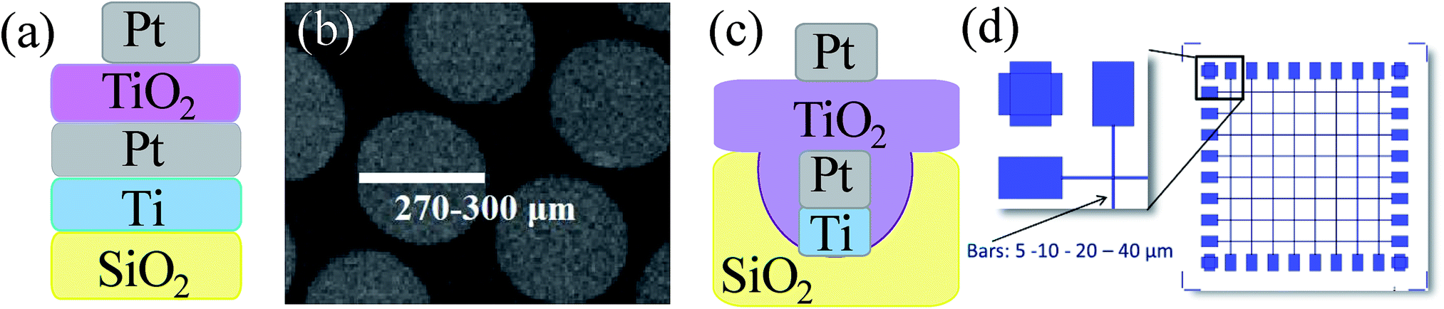 | ||
| Fig. 1 (a) Schematic representation of a memristive cell; (b) SEM image of an array of Pt top dishes (270–300 μm in diameter) in a fabricated device; (c) schematic representation of a memristive unit in a crossbar array; (d) schematic representation of a crossbar array. | ||
Numerous materials were reported to display resistive switching, including a large array of oxides,11,13,14 perovskites,15 nitrides,16 selenides,17 and organic compounds.18–20 Among a wide range of materials, TiO2 has been chosen as an active switching layer to fabricate a memristive cell based on the following desired properties. The material should be robust toward environmental and operation conditions. For reliable performance, the device must have a uniform switching layer with an identical response at any given point of operation. Macro- and microscale defects, such as clusters, holes, and cracks in the film have to be eliminated in order to avoid short circuits in a memristive cell. Thus, a dense material constituted of fine grains is expected to have the lowest surface roughness and is the most promising. Depending on the mechanism, the size scale of the resistance switch may vary from bulk (tens of nanometer) to interfacial surface regimes.12 Even though the development of thin films with exceptionally low (<3 nm) thickness may be beneficial for the switch, it also makes them mechanically vulnerable to tunneling and hot-spot issues. On the other hand, TiO2 layers tens of nanometers thick require an electroforming procedure that may damage electrodes during the evolution of molecular oxygen. Thus, “pre-activated” materials that already contain oxygen vacancies may be beneficial for stable performance of the device. Finally, the memristive response strongly depends on material and electrical input parameters; therefore, the material composition has to be reproducible to predict and acquire the desired memristive response.
For successful memristor development, the top and bottom electrode materials have to be chosen carefully, since the memristive behavior may be directly influenced by the electrode's work function, electronegativity, oxygen affinity, interface reactivity, and solid-state diffusion.21,22 For instance, in the case of the inert top electrodes, such as Au, Pt, and Ru, the switch relies on the presence of oxygen vacancies in the semiconductor layer, whereas Ag and Cu electrodes generate corresponding filaments under the electric field.23 Moreover, the bottom electrode, onto which the semiconductor layer is deposited by the sol–gel process, has a potential to influence the preferential orientation of the material, controlling charge transport through the film.24,25
2. Experimental
2.1. Syntheses
![[thin space (1/6-em)]](https://www.rsc.org/images/entities/char_2009.gif) :2 (sol:alcohol) volume ratio under N2.
:2 (sol:alcohol) volume ratio under N2.2.2. Fabrication of switching cells
SiO2/Ti (5 nm)/Pt (50 nm) bottom electrode fabrication, substrates preparation, cleaning, and a spin coating recipe for Ti sol deposition were reported elsewhere.27 The deposition of platinum circular shaped electrodes (270–300 μm in diameter, 40–50 nm thick) was performed by the electron beam evaporation, reported previously.282.3. Fabrication of cross-bar architectures
SiO2/Ti (5 nm)/Pt (50 nm) bottom rode electrodes (5–40 μm) for crossbar architecture were obtained starting from a flame fused quartz 6′′ wafer with a thickness of 650 μm. A standard UV lithography for a lift-off process was carried out, 50 nm bulk etching was performed by Reactive Ion Etching, followed by a multilayer (5 nm of titanium and 50 nm of platinum) deposition by the electron beam technique, yielding SiO2/Ti (5 nm)/Pt (50 nm) structures. The wafers were cut in dices of 1.5 cm × 1.5 cm. The prepared electrodes were brushed and rinsed with acetone, 2-propanol, followed by rinsing with D.I. water, and finally dried with nitrogen. Afterward, the electrodes were etched with oxygen plasma right prior to the spin coating deposition. A spin coating recipe was published previously.27Top platinum (40 nm) rode electrodes were deposited by the electron beam evaporation. Pt films were evaporated from a platinum rod (99.99% purity, supplied by Umicore) in a vacuum chamber using an e-beam evaporator EBX-16C (Ulvac). The pressure during the deposition was adjusted in a 2 ÷ 3 × 10⁻⁷ torr range with an evaporation rate of 0.1 nm sec−1. In each evaporation process TiO2 films (1.5 cm × 1.5 cm) were patterned using a shadow mask with rode-shaped patterns.
2.4. Characterization
AFM measurements were performed using a Cypher AFM (Asylum Research, Santa Barbara, CA) in an AC mode in air. AC200 silicon cantilevers (Olympus) with a nominal force constant of 9 N m−1 were used, acquiring images of different areas, ranging from 200 × 200 to 10000 × 10000 nm2. Scans were acquired and leveled line-by-line using the Asylum provided software. Data were analyzed and rendered with ImageJ.29
X-Ray diffraction data were acquired on an Italstructures IPD3000 instrument equipped with a Cu anode source (fine focus) operating at 40 kV and 30 mA. A multilayer monochromator was used to suppress k-beta lines from the incident radiation with a dual fixed-slit setup (100 μm) to reproduce a quasi-parallel beam. Diffraction spectra were acquired in a reflection geometry (fixed omega = 1°) over a 1–121 degree range by means of an Inel CPS120 curved position sensitive detector, working with a 15% ethane/argon mixture at 6 bar. The instrument was preliminarily calibrated by means of a NIST 660b LaB6 standard reference material.
XPS analyses were performed using Kratos Axis UltraDLD and Scienta ESCA-200 instruments both equipped with a hemispherical analyzer and a monochromatic Al Kα (1486.6 eV) X-ray source, in a spectroscopy mode. The emission angles between the axis of the analyzer and the normal to the sample surface were 0°. For each sample, Ti 2p, O 1s, C 1s and Si 2p core lines were collected. XPS quantification was performed using the instrument sensitivity factors and the high resolution scans. Charge compensation, when needed, was achieved using a charge neutralizer located at the bottom of the electrostatic input lens system and all core level peak energies were referenced to the saturated hydrocarbon in C 1s at 285.0 eV.
Raman spectra were collected using a Labram Aramis (Horiba Jobin-Yvon) equipped with an optical microscope and a 100× objective. A helium–neon laser (632.8 nm) was used for the excitation of the Raman signal with appropriate holographic notch filters in order to eliminate the laser line after excitation. The slit width of the spectrometer was typically set at 50 μm. A holographic grating with 1800 grooves per mm was used for the collection of all Raman spectra with a resolution of 1 cm−1. Spectral analysis and curve fitting were performed with a LabSpec Spectroscopy software.
The optical parameters such as thickness and refractive index at 632.8 nm were obtained by ellipsometry measurements using an AUTOEL IV ellipsometer. The ellipsometry data were acquired at a fixed wavelength and a fixed angle of 70°. Thickness measurements were carried out by the profilometry technique using a Tecno P6 mechanical profilometer. The reported values are an average of 5 measurements with an error of about 10%.
NEXAFS experiments were carried out at the BEAR end station (BL8.1L), at the left exit of the 8.1 bending magnet of the ELETTRA synchrotron facility in Trieste (Italy).30,31 NEXAFS spectra were collected in a total electron yield (TEY) mode (i.e., drain current mode) at the edge of Ti L2,3 and O K and normalized to the incident photon flux. Spectral energies were calibrated by referring to the 4f7/2 Au core level, which was obtained from an Au(100) sputtered sample (i.e., carbon free). The synchrotron beam was elliptically polarized with dominating components lying in the horizontal (H) plane and the corresponding ellipticity, defined as ε = |![[E with combining right harpoon above (vector)]](https://www.rsc.org/images/entities/i_char_0045_20d1.gif) V|2 × |H|−2, is equal to 0.1 (V stands for vertical plane and ε = 1 (0) for circularly (linearly) polarized light). Throughout the measurements, the incidence angle of the light with respect to a sample's surface plane has been kept fixed at 10°. To correctly process the acquired data, each absorption spectrum was first normalized to the drain current, which was measured on an optical element (refocusing mirror) placed along the beam-line; then, normalized to the absorption spectrum attained under the same experimental conditions and energy range, on an Au(100) sputtered sample. The energy scale of each single spectrum was re-calibrated taking into the account the energy fluctuation of characteristic absorption features measured on the refocusing mirror.
V|2 × |H|−2, is equal to 0.1 (V stands for vertical plane and ε = 1 (0) for circularly (linearly) polarized light). Throughout the measurements, the incidence angle of the light with respect to a sample's surface plane has been kept fixed at 10°. To correctly process the acquired data, each absorption spectrum was first normalized to the drain current, which was measured on an optical element (refocusing mirror) placed along the beam-line; then, normalized to the absorption spectrum attained under the same experimental conditions and energy range, on an Au(100) sputtered sample. The energy scale of each single spectrum was re-calibrated taking into the account the energy fluctuation of characteristic absorption features measured on the refocusing mirror.
2.5. Electrical testing
Voltage-controlled electrical testing was performed with a custom setup composed of a stereoscopic microscope SKU:H800 (AmScope), micromanipulators with tungsten probes, a 2410 High Voltage SourceMeter (Keithley) connected to a PC through a GPIB card and controlled by a software user interface (Labview, National Instruments).28 Current-controlled electrical testing was accomplished with NI PXIe-1073 chassis connected to a PC through a PCI-express card and controlled by a software user interface developed within the Labview environment. The chassis was equipped with a NI-PXIe-4139 source measure unit capable of current or voltage controlled source and measure. The I–V curves were recorded in an ambient atmosphere at RT.3. Results and discussion
Preparation of TiO2 thin films by the sol–gel method consists of five main steps (Fig. S1†): (I) preparation of a sol; (II) oxygen plasma electrode etching; (III) spin coating deposition of the sol onto the electrode; (IV) curing; (V) annealing.These five key steps control the thickness, surface roughness, crystallinity, stoichiometry, substrate adhesion, and purity of the thin films. Through optimization in these stages, we produced desirable building blocks for memristor devices and identified the material features that affect the memristive response, suggesting further ideas for optimization of the material.
Among different growth processes, the sol–gel route has been chosen to fabricate TiO2 thin films since it provides a versatile control over the crystalline phase and thickness of films.32 The sol–gel method in conjunction with spin coating grants a considerable advantage over cluster source deposition, feasibly providing highly dense materials with a low surface roughness.33 Additionally, the stoichiometry of the material may be controlled by introduction of dopants into the sol or processing the films in a selected atmosphere; in contrast, stoichiometry control is extremely challenging using laser ablation, radio frequency, and magnetron sputtering.34 Moreover, the low-cost wet chemistry method enables lower cost deposit than the more expensive atomic layer deposition method.
Close-packed TiO2 grains are known to form from a three-dimensional polymeric skeleton, whose growth is favorable from titanium alkoxides with low water content, low hydrolysis rate, and high concentration of Ti(OR)4 in the reaction mixture.35 In order to achieve a low hydrolysis rate, the chelating agents are introduced to the reaction mixture.
The stabilized resulting sol ensures the reproducibility of the obtained material properties. Ti(i-OPr)4 was used as a precursor with the assistance of 2-aminoethanol as a chelating agent, in conjunction with 2-methoxyethanol or ethanol, for routes 1 and 2, correspondingly.26,27 Among conventional chelating agents, 2-aminoethanol has been chosen due to a relatively low boiling point, ensuring efficient removal from the film during the heat treatment stage. Table 1 summarizes the TiO2 thin films prepared from two different sol compositions.
The films obtained by the 1st route and annealed in the atmosphere of air, 1TPA, were comprehensively studied by SEM, FE-SEM, XPS, FT-IR, micro-Raman, and prism coupling m-line spectroscopy in conjunction with transmittance, and profilometry measurements, and the results were reported elsewhere.27,28 In summary, the 1st route led to the formation of uniform, flawless and dense films of about 52 nm thick (double layer) consisting of anatase TiO2 grains. The 1st route uses 2-aminoethanol as a chelating agent in conjunction with 2-methoxyethanol as a coordinating solvent. In order to demonstrate the effect of 2-methoxyethanol in the sol, the reaction mixture was prepared in presence of absolute ethanol instead of 2-methoxyethanol (route 2). SEM images (not shown) displayed the absence of any noticeable micro defects at the magnification up to 12000 on the surface of 1 and 2 layered samples prepared by route 2 on Pt/Ti/SiO2 substrate. Therefore, considering the absence of the defects observed by SEM, the exclusion of 2-methoxyethanol from the sol may be beneficial since it allows elemination of a toxic solvent and lowering a process cost. Based on these promising outcomes, a memristive cell with a Pt top dish electrode was fabricated and the results of electrical testing are discussed below.
The second step of thin film preparation is cleaning and modification of the substrates. For a reliable memristive response, it is essential to remove carbon-based pollutants from the surface of SiO2/Ti/Pt electrode by cleaning and oxygen plasma etching procedures, as reported previously.27,28 In addition to a cleaning function, oxygen plasma treatment is essential for the improvement of SiO2/Ti/Pt electrode adhesion to the titania sol. In our previous studies,27 we observed the peeling of TiO2 layer in the absence of oxygen plasma etching. For the transmittance and m-line measurements, the deposition of the sol (route 1) on silica substrates was performed. The improvement in the adhesion of silica to the titania sol may be achieved by placing the substrates in distilled water overnight, by 30 minutes treatment with fresh piranha solution or by oxygen plasma etching.27
The third key step in thin film fabrication is deposition of the titania sol by spin coating. Spin coating provides the control over homogeneity of the resulting film thickness and even a size of nanoparticles.36 In our studies, we have performed the spin coating in a clean room; the sol prepared in a conventional lab was filtered through a Teflon filter prior to the deposition. Static dispensing method was used and the whole area of the electrode was covered by sol prior to the start of spinning. We found that 50 s spinning time at 3000 rpm was sufficient to evaporate 2-methoxyethanol. For the fourth step, the resulting films were cured at 150 °C for 1 h.27
Annealing is the fifth key step in the thin film formation. Thermally cured TiO2 thin films prepared by the route 1 were annealed in an atmosphere of air at 400 °C for 1 h with a heating/cooling rate of 1 °C min−1. Thickness, refractive index, and porosity of the annealed films, 1TPA, were studied by ellipsometry and profilometry (Table 2). Ellipsometry measurements were carried out both on a bare electrode (SiO2/Ti/Pt) and on 1TPA (1 and 2 layered) in order to determine the refractive index (RI) at 632.8 nm and thickness of the films. The bare electrode yielded an RI value of n = 2.07 + i4.24 @ 632.8 nm. The obtained values of RI and thickness of 1TPA with a different number of layers are reported in Table 2. Profilometry measurements were performed in order to confirm the thickness value obtained through ellipsometry measurements (Table 2). For 1TPA (1 and 2 layers) the thickness values were estimated to be 30 and 52 nm, correspondingly, and are in agreement with the optically derived values.
| Sample set label | Na | Profilometryb | Ellipsometryc | Porosityd | |
|---|---|---|---|---|---|
| Thickness [nm] | n | Thickness [nm] | |||
| a Number of layers.b Thickness values obtained by profilometry measurements.c The results were evaluated by the ellipsometry technique (at λex = 632.8 nm), an average of 5 measurements.d Porosity was estimated from optical parameters. | |||||
| 1TPA | #1 | 30 | 2.00 | 32 | 0.3 |
| #2 | 52 | 2.24 | 60 | 0.16 | |
The porosity of 1TPA was evaluated from optical measurements as previously described in literature.27 The results reported in Table 2 revealed the decrease in the porosity of the films after annealing with respect to the porosity of the “green” samples (P = 0.4–0.6) studied in,27 suggesting that heat treatment at 400 °C leads to dense TiO2 structures.
Atomic force microscopy (AFM) was performed to establish the surface roughness of the resulting films. The AFM images acquired from 1TPA at different magnifications (from 200 × 200 nm2 to 10 × 10 μm2) show exceptionally smooth surfaces with roughness (Rq) of about 0.7 ± 0.1 nm (Fig. 2). Additionally, no defects, such as holes, were observed by AFM surface profile measurements. The resulting smooth surface is beneficial for a consistent electric response along the film in a corresponding memristive cell.
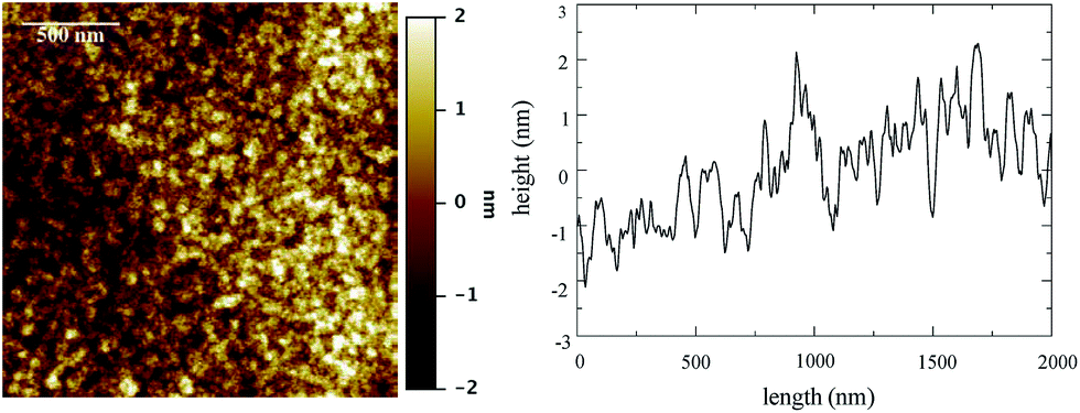 | ||
| Fig. 2 AFM image of 1TPA, at 2 × 2 μm2, (left) and surface profile (right). Rq is 0.75 ± 0.08 nm at this acquisition scale. False color vertical scale from −2 to 2 nm. | ||
Further investigation of 1TPA (2 layers) was performed by X-ray diffraction measurements (XRD). The XRD analysis of 1TPA was challenging, owing to the low thickness of TiO2 films and relatively high penetration depth of the Cu-kα X-ray radiation in the material (∼tens of microns). Therefore, a careful calibration of an optimal incidence angle of the primary X-ray beam (omega) had to be performed. Lower incidence angles allow the optimization of the signal from TiO2 thin films with respect to SiO2/Ti/Pt electrode, simultaneously reducing the total signal statistics. Thus, an omega angle of 1° had been chosen to acquire the data as the best compromise.
The diffraction spectrum collected on 1TPA is shown in Fig. 3. The broadened peak centered at ∼21° is typical of an amorphous phase and attributed to a SiO2 substrate. The sharp diffraction peaks at 25.5°, 38°, 48.3°, 54°, 55.3° and 63° were indexed with the (101), (004), (200), (105), (211) and (204) well-crystallized anatase reflections, respectively.37 The remaining diffraction peaks were assigned to a Pt cubic phase. Most importantly, no additional diffraction peaks corresponding to other polymorphs of TiO2, such as rutile and brookite, were observed.
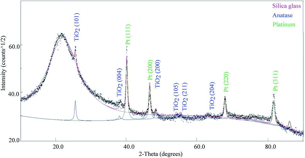 | ||
| Fig. 3 X-ray diffraction data collected on the sample 1TPA (2 layers), with indexing of relevant phases. | ||
XRD data were modeled by means of a full-pattern approach based on the Rietveld method as implemented in the Maud software.38 The sample model is a three phase mixture, accounting for crystalline platinum, anatase TiO2, and amorphous silica from the substrate. Modeling parameters are included, in addition to the crystal phases volume fractions and the scale factors, and the average crystallite sizes for both Pt and TiO2 phases. The experimental diffraction intensities originating from Pt slightly differ from those calculated from the reference literature structure, which may be attributed to a possibility of preferred orientation. Alternatively, any significant preferred orientation can be excluded for the TiO2 layer, considering a good agreement between experimental and calculated intensities.
During the annealing step, control over crystallinity, the desired stoichiometry, and purity of the film may be achieved. At this step, the introduction of oxygen vacancies in the TiO2 layer may be performed by heat treatment of the film in vacuum.22 The resulting thin films containing a substantial number of oxygen vacancies have a potential to yield a memristive response in an absence of the electroforming stage, which is not possible for the samples annealed in an atmosphere of air.39 In our previous studies, changes in a chemical composition of the TiO2 layer were introduced by annealing the samples in air, vacuum and oxygen (Table 3).28 The preliminary data on electroforming and memristive response were studied in order to find the correlation of electrical outcomes with the chemical composition of TiO2 thin films.28
| Sample | Atmosphere of annealing |
|---|---|
| a The oven chamber was purged with oxygen (5 L min−1) for 10 min prior to the heat treatment.b The oven chamber was flushed with nitrogen for 2 min at 35 °C prior to the heat treatment in vacuum (350 ± 100 Pa). | |
| 1TPA-Si | Air (Si-contaminated oven) |
| 1TPA | Air (clean oven) |
| 1TPO | Oxygena |
| 1TPV | Vacuumb |
Fig. S2† shows XPS surveys of TiO2 samples annealed in air, oxygen, and vacuum, 1TPA, 1TPA-Si, 1TPO, and 1TPV. It was discovered that the silicon contamination originated from the oven (Fig. S2,† 1TPA-Si). To prevent this, the samples were annealed in a different compartment (Fig. S2,† 1TPA). Although the problem with a Si contamination was successfully resolved, the produced samples still suffered with contamination by carbon and nitrogen, predominantly on the surface.28
The core lines spectra of O 1s and Ti 2p acquired from the four samples are shown in Fig. 4. The O 1s core line profiles of 1TPA, 1TPA-Si, and 1TPO display two peaks at 531.4 eV and 529.7 eV. The first one is attributed to oxygen from the surface contamination (Si–O, C–O),28 whereas the second peak corresponds to O–Ti bonding.40 For the 1TPV sample, the peak that arises from O–Ti is slightly shifted toward higher energies, 529.95 eV, which may be ascribed to the contribution of oxygen vacancies.41 For all the samples, the Ti 2p core line profiles are identical with a doublet at 458.50 and 464.21 eV, corresponding to the Ti 2p3/2 and Ti 2p1/2 spin–orbit peaks of TiO2.40 No signals from lower oxidation states of titanium, for example, Ti3+ at 457.1 eV, were observed.41
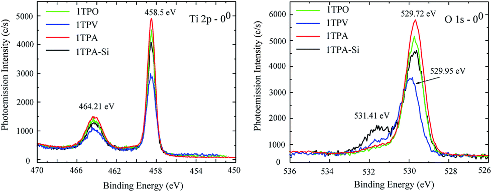 | ||
| Fig. 4 XPS core lines spectra of Ti 2p (left) and O 1s (right) acquired from 1TPA, 1TPA-Si, 1TPV, and 1TPO at 0° probing angle. | ||
Structural investigation of the samples prepared by route 1 and annealed in a variety of atmospheres was performed by micro-Raman spectroscopy, providing the evaluation of the phase composition as well as a degree of order–disorder at a short range of TiO2 crystalline structures based on relative intensity, width, and displacements of vibrational modes. Raman spectra of all TiO2 thin films are shown in Fig. 5. For all the spectra, the 5 vibrations of anatase phase were observed: (a) Eg, related to the symmetric stretching of Ti–O–Ti, (b) B1g, caused by the symmetric bending of O–Ti–O and (c) A1g peak associated with the asymmetric bending of O–Ti–O.27,42 Moreover, no signals arising from other polymorphs of TiO2, brookite and rutile, were observed in Fig. 5. The latter is in agreement with the presence of solely anatase phase observed by XRD.
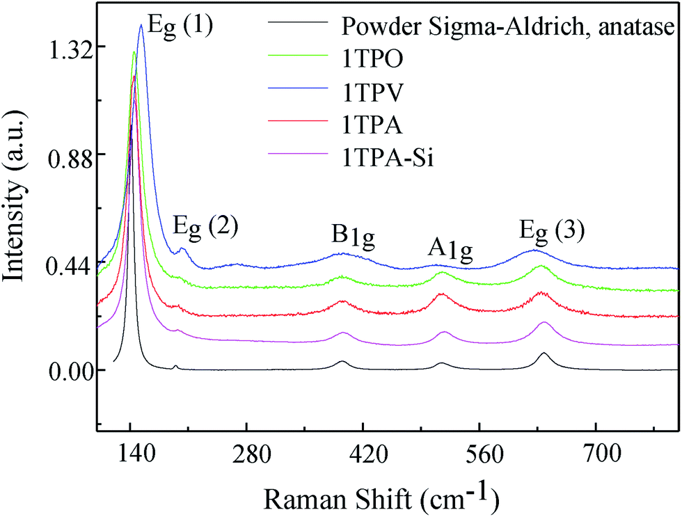 | ||
| Fig. 5 Raman spectra acquired from TiO2 thin films annealed in a variety of atmospheres together with the model Raman spectrum obtained from TiO2 powder (Sigma Aldrich). | ||
In order to evaluate the role of the atmosphere during the temperature treatment, the Raman spectrum from TiO2 commercial powder (anatase, Sigma-Aldrich) was acquired as a model. The most intense peak Eg (1) for all the samples, 1TPA, 1TPA-Si, 1TPO, and 1TPV, is blue-shifted and broadened compared to the model spectrum acquired from the commercial powder (Fig. 5). The shift of Eg (1) in the thin films may be attributed to a variety of effects, including disorder induced defects and phonon confinement.42,43 Additionally, the broadening of the peaks may be associated with a size of crystallites and its distribution.44
Simultaneously, the red shift and broadening of B1g, A1g, Eg (3) of 1TPV spectrum, may be caused by several competing mechanisms, including the nonstoichiometry due to oxygen vacancies, disorder induced defects, and phonon confinement effects.45–47 Insofar as the reduced heat transfer in vacuum could affect a size of the crystallites compared to the samples processed in air or oxygen, broadening of Raman bands can be attributed to the variation in the size of crystallites.43,48
In order to further investigate the effect of the annealing atmosphere on the structural properties of the thin films, X-ray absorption spectroscopy (XAS) was performed. In the following, a brief summary of the TiO2 valence and conduction bands' nature is given, providing a complete understanding of the XAS spectra reported in Fig. 6. The valence band is mainly formed by O 2p (mostly O 2p-derived) levels hybridized with Ti 4s and 4p orbitals.49 The conduction band (probed by the XAS experiment presented here) is formed by Ti 3d, 4s and 4p, and O 2p orbitals. The crystal field induced by surrounding oxygen atoms splits Ti 3d orbitals in two sub-bands, namely t2g and eg. Due to the specific orientation toward O 2p orbitals of the surrounding oxygen and larger hybridization with O, the eg transition peak is slightly more intense than the t2g transition peak and highly sensitive to the crystal structure and coordination.
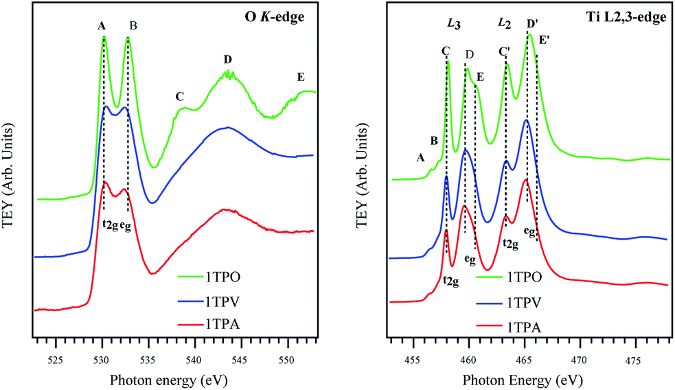 | ||
| Fig. 6 O K-edge X-ray absorption spectra of TiO2 samples annealed in air, vacuum, and oxygen, 1TPA, 1TPV, and 1TPO, correspondingly (left); Ti L2,3-edge X-ray absorption spectra of TiO2 samples annealed in air, vacuum, and oxygen, 1TPA, 1TPV, and 1TPO, respectively (right). | ||
Fig. 6 (left) provides a comparison of O K-edge XAS spectra of the sol–gel derived TiO2 samples annealed in different conditions. In agreement with the previous works,50–54 all the TiO2 samples exhibit two main peaks centered at ∼531 and 534 eV (labeled as A and B) and additional structures at a higher energy (labeled as C, D, and E). The two main peaks A and B are attributed to the transition from O 1s into t2g and eg bands, respectively, induced by the crystal field. Other features at higher energy (C, D, and E) are attributed to the transition from the O 1s level to the O 2p and Ti 4s/4p antibonding bands.
All the spectra in Fig. 6 are very similar (especially lower energy regions), indicating that the electronic structures of the TiO2 samples studied in this work are alike. Nevertheless, the peaks in the spectra of air and vacuum annealed TiO2 films, 1TPA and 1TPV, are broadened and less resolved compared to the bands arising from oxygen annealed films, 1TPO. Such a broadening in the spectra is correlated to the signal contribution from amorphous solids, due to slight variations in bond lengths and angles. Additionally, a significant decrease in the distance between the peaks A and B from ∼2.6 to 2.0 eV in 1TPA and 1TPV with respect to 1TPO was observed. Such a decrease of the ligand field splitting (i.e. the energy difference between the t2g and eg originated transition) leads to a shift of the peak B to a lower energy and is compatible with a slightly different and inhomogeneous chemical environment together with a less defined structure in the samples annealed in air and vacuum, 1TPA and 1TPV, with respect to the one annealed in oxygen, 1TPO. The shift of the peak B toward a lower energy is consistent with a higher sensitivity to the local environment of the eg transition. A small shift of the peak A by ∼0.4 eV toward a higher energy is observed for 1TPA and 1TPV samples with respect to 1TPO. This can be attributed to a slightly larger band gap, which is probably correlated to a small intermixing of anatase with amorphous phase. However, no amorphous phase is detectable in the sample annealed in oxygen, 1TPO.
In contrast to the O K-edge spectra reported in Fig. 6 (left), the Ti L2,3-edge spectra shown in Fig. 6 (right) are considerably more structured and complex. The transitions in the Ti L2,3-edge spectra involve excitations from Ti 2p levels to Ti 3d states of a conduction band. As suggested by de Groot et al.,55,56 the complexity of the spectra mainly originates from the interaction between Ti 3d electrons (that are poorly screened) and Ti 2p core hole. Due to the spin–orbit coupling of Ti 2p orbitals, all the peaks from the samples are split into two groups L3 and L2 separated by ∼5.5 eV. In addition to the spin–orbit coupling, the crystal field splits the 3d level (i.e. L3 and L2) into two sub-bands t2g and eg (as in the O K-edge spectra). Apparently, all the spectra reported in Fig. 6 (left) are relatively similar and clearly indicate that the major contribution to the spectra is ascribable to the anatase phase. Only 1TPO shows a small shift of the C and C′ transitions to a higher energy that is attributed to a slightly different band gap with respect to the other two samples that show a minor contribution of an amorphous phase to the anatase phase.
For all the samples, the eg band in the L3 as well as in the L2 regions is split additionally into two peaks labeled as D, E and D′, E′, respectively. This split is commonly attributed to a distortion of crystal symmetry from an ideal octahedral Oh geometry to D2h and D2d geometries.57 Moreover, the splitting can also be correlated to a different coupling of electronic and vibrational states (i.e. Jahn–Teller effect) and to different degrees in the long-range order.57
In Fig. 6 (right) the D/E ratio clearly shows that the anatase is a predominant phase in all the samples, even if for 1TPV and 1TPA the presence of an amorphous phase cannot be excluded, which would be in agreement with the increased broadening of the peaks. The spectrum of 1TPO shows shifts of the components D, E and D′, E′ to higher energies, by 0.3 eV and 0.45 eV, respectively. Moreover, different energy shifts, together with a higher broadening and a change in the D/E ratio, can be attributed to a higher degree of crystallinity and different symmetry distortion around Ti atoms in 1TPO with respect to 1TPV and 1TPA. These considerations are also consistent with a shift of the L2 eg transition toward a lower energy for 1TPA and 1TPV.
All the spectra reported in Fig. 6 (right) show two additional features A and B in a lower energy range at ∼457 eV that on the base of theoretical calculations performed by de Groot et al.55,56 and Finkelstein et al.58 are attributed to strong interactions between poorly screened Ti 3d electrons and Ti 2p core hole, together with sharp features presented in Ti 3d partial density of states.
The combined data obtained by Raman and XAS suggest that 1TPA, 1TPV, and 1TPO display modest differences in the TiO2 anatase crystal structure and, thus, may influence electrical properties of the materials. Most ordered, coherent and defined structure was detected in 1TPO, whereas the highest degree of disorder and defects was observed in 1TPV. Therefore, annealing represents a powerful tool for fine tuning of the TiO2 structure.
The electrical studies were performed with Pt both as top and bottom electrodes. The memristive response of the cell (Fig. 1) is dependent on semiconductor and electrode materials and on electrical input parameters, including applied voltage or current, frequency, and environment.39 Therefore, the memristive behavior of Pt/TiO2/Pt can be pre-programmed at the electroforming step. For instance, the bipolar or unipolar switching behavior can be tuned by adjusting an appropriate compliance value of current during the activation. The electroforming parameters have to be chosen carefully both to ensure a stable switching behavior and to avoid a breakdown of the material.
The fabrication of the memristive cell was performed by the deposition of Pt top electrode dishes (270–300 μm in diameter, 40–50 nm thick) on 1TPA-Si, 1TPA and 2TPA building blocks by the electron beam evaporation method (Fig. 1b). Electrical characterization was performed on 1TPA-Si and 1TPO samples with Pt dish and Pt tip top electrodes, correspondingly, and reported elsewhere.28 Briefly, it was found that 1TPO sample failed to perform a stable memristive behavior after an electroforming recipe and resulted in a breakdown. More likely, a highly ordered crystal structure with an absence of the defects is responsible for such a poor performance. Meanwhile, 1TPA-Si showed a steady memristive response without a collapse; thus, only the samples annealed in the atmosphere of air are discussed further on.
Driven by the promising results reported in28 current and voltage-controlled activations were tested. Fig. S3† shows gradual voltage-controlled electroforming performed on virgin insulating 1TPA-Si with a resistance of gigaohms. At first, eight negative sweeps from 0 to −5.5 V were applied with a compliance current of 20 mA and 60 s duration (Fig. S3†). Even though the compliance current was not achieved, with every sweep the current value at −5.5 V increased, suggesting a gradual formation of a memristive channel. Then, four sweeps from 0 to −6 V and other four from 0 to −6.5 V were performed with an absence of any noticeable change in a current value. Thus, the voltage window of a sweep was opened up to −8 V and the compliance current of 20 mA was finally achieved, resulting in a SET state (Fig. S3, right†). A RESET state was attained during a positive sweep from 0 to +1.5 V.
Based on the data above, a value of −8 V has to be achieved during the negative sweep in order to fully open the channel. Once the channel is formed, the voltage window can be narrowed to a −5 to +2 V range (Fig. 7a and b). Under these conditions, a hysteresis loop was observed with a (v, i) = (0, 0) pinch.
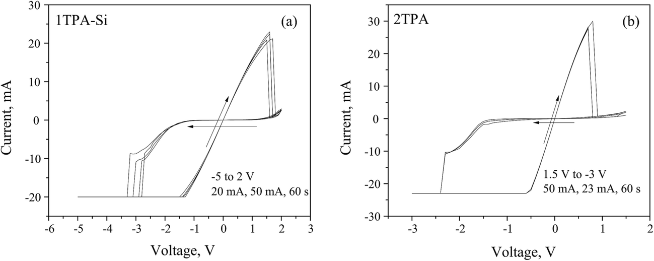 | ||
| Fig. 7 Memristive responses from (a) 1TPA-Si, 5 cycles; and (b) 2TPA, 3 cycles, after a voltage-controlled electroforming. | ||
The observed asymmetrical switch suggests that the device is a non-ideal memristor, since an ideal memristor behavior is symmetrical.59 The asymmetry of the switch may be attributed to the asymmetry of the device. For instance, the semiconductor layer may contain more oxygen close to a bottom electrode, since it was treated with oxygen plasma, resulting in an uneven distribution of oxygen vacancies at the electroforming stage.39 In addition to that, the annealing atmosphere and the environment, in which the measurements are performed, may generate the asymmetry of the material composition, and thus, the response. Since 1TPA-Si displays a linear I–V relationship through the origin, the behavior can be assigned to a generic class of memristors.59
Considering the suitable characteristics of 2TPA layer, the corresponding memristive cell with Pt dishes as top electrodes was fabricated and the electrical testing was performed after a voltage-controlled electroforming (Fig. 7b) with a recipe similar to the one described above. The nature of the electrical behavior is very similar to 1TPA-Si, except for the voltage window, that is narrowed in the case of 2TPA. Additionally, the endurance is reduced for 2TPA compared to the 1TPA-Si based memristive cell.
Apart from the voltage-controlled electroforming, the current-controlled activation was tested on 1TPA films with dishes and a crossbar architecture (Fig. 1).
The current-controlled electroforming was performed on 1TPA with a Pt top dish as a top electrode by applying −500 μA with a 100 nA step and a compliance of 15 V, that was followed by a sweep of 500 μA with a 100 nA increment and a compliance of 15 V (Fig. S4†).
Similar to that, the current-controlled electroforming was performed on the crossbar architecture by applying 200 μA with a 500 nA step and a compliance of 15 V. The resulting switching behavior displayed higher stability, durability, and low power of operation. The nature of the memristive switch differs from the one obtained for the voltage-controlled electroforming (Fig. 7 and 8, right). Clearly, apart from the voltage range, the I–V curve becomes nonlinear; suggesting that the nature of the memristor is altered compared to the voltage-controlled electroforming. Overall, the device can be classified as a non-ideal bipolar extended memristor, as suggested by Chua.59 Upon the current-controlled electroforming, the switch is more symmetrical than the one observed after the voltage-controlled activation. Although in a virgin state the sample had a resistance of 100 kΩ, the SET was observed with a resistance of 20 kΩ, whereas the RESET displayed a resistance of 1.1 MΩ; giving RON/OFF ∼ 55. The device based on 1TPA with a Pt top dish electrode displayed at least 500 consecutive switching cycles (Fig. S5†). Overall, the electroforming input parameters and the architecture of the device influence the memristive switch behavior.
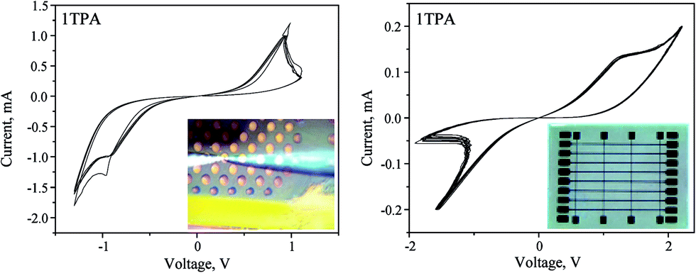 | ||
| Fig. 8 Memristive response from 1TPA dishes (left, 4 cycles) and crossbar (right, 10 cycles) after a current-controlled electroforming. | ||
Previously observed structural changes in a memristive cell during the measurements were attributed to the evolution of molecular oxygen with a subsequent damage of the Pt top dishes electrodes.28 The “soft” electroforming reported herein may be beneficial for the slow and gentle O2 evolution, thus, avoiding the damage of electrodes.
4. Conclusions
Herein, the fabrication of SiO2/Ti/Pt/TiO2 by the sol–gel method and the corresponding memristive cells is reported. The influence of the sol's chemical composition and processing parameters on the final properties of TiO2, and therefore on the memristive response, was thoroughly studied by micro-Raman and transmission spectroscopy, profilometry, ellipsometry, X-ray photoelectron spectroscopy (XPS), atomic force microscopy (AFM), X-ray absorption and diffraction spectroscopies (XAS and XRD). It was shown that the minor changes in the key steps of the TiO2 thin films fabrication affect the electrical response of the corresponding memristive cells. Moreover, the electroforming input parameters together with the architecture of the device influence the memristive switch behavior. All together, they provide a handful tool for the desirable electric outcome.Acknowledgements
The authors are thankful to Dr Laura Pasquardini (University of Trento, Department of Industrial Engineering), Dr Cecilia Pederzolli (FBK, LaBSSAH), Prof. Maurizio Ferrari (CNR-IFN, CSMFO Lab), and Prof. Luca Lutterotti (University of Trento, Department of Industrial Engineering) for valuable suggestions. The authors are grateful to Mr Giuseppe Resta for the development of a software user interface (Labview, National Instruments). This research was performed in a framework of the “Grandi progetti 2012” PAT: “Developing and Studying novel intelligent nano Materials and Devices towards Adaptive Electronics and Neuroscience Applications” – MaDEleNA Project.References
- G. E. Moore, Proc. IEEE, 1998, 86, 82–85 CrossRef.
- F. Pan, S. Gao, C. Chen, C. Song and F. Zeng, Mater. Sci. Eng., R, 2014, 83, 1–59 CrossRef.
- J. S. Meena, S. M. Sze, U. Chand and T.-Y. Tseng, Nanoscale Res. Lett., 2014, 9, 526 CrossRef PubMed.
- E. Gale, Semicond. Sci. Technol., 2014, 29, 104004 CrossRef.
- S. Gao, F. Zeng, M. Wang, G. Wang, C. Song and F. Pan, Sci. Rep., 2015, 5, 15467 CrossRef CAS PubMed.
- J. Borghetti, G. S. Snider, P. J. Kuekes, J. J. Yang, D. R. Stewart and R. S. Williams, Nature, 2010, 464, 873–876 CrossRef CAS PubMed.
- S. H. Jo, T. Chang, I. Ebong, B. B. Bhadviya, P. Mazumder and W. Lu, Nano Lett., 2010, 10, 1297–1301 CrossRef CAS PubMed.
- D. B. Strukov, G. S. Snider, D. R. Stewart and R. S. Williams, Nature, 2008, 453, 80–83 CrossRef CAS PubMed.
- A. Moballegh and E. C. Dickey, Acta Mater., 2015, 86, 352–360 CrossRef CAS.
- J. J. Yang, D. B. Strukov and D. R. Stewart, Nat. Nanotechnol., 2013, 8, 13–24 CrossRef CAS PubMed.
- K. M. Kim, T. H. Park and C. S. Hwang, Sci. Rep., 2015, 5, 7844 CrossRef CAS PubMed.
- J. Joshua Yang, F. Miao, M. D. Pickett, D. A. A. Ohlberg, D. R. Stewart, C. N. Lau and R. S. Williams, Nanotechnology, 2009, 20, 215201 CrossRef CAS PubMed.
- W.-Y. Chang, Y. C. Lai, T. B. Wu, S. F. Wang, F. Chen and M. J. Tsai, Appl. Phys. Lett., 2008, 92, 022110 CrossRef.
- Y. Yang, P. Sheridan and W. Lu, Appl. Phys. Lett., 2012, 100, 203112 CrossRef.
- H. Nili, S. Walia, S. Balendhran, D. B. Strukov, M. Bhaskaran and S. Sriram, Adv. Funct. Mater., 2014, 1–10 Search PubMed.
- C. Chen, Y. C. Yang, F. Zeng and F. Pan, Appl. Phys. Lett., 2010, 97, 083502 CrossRef.
- Y. T. Huang, C. W. Huang, J. Y. Chen, Y. H. Ting, K. C. Lu, Y. L. Chueh and W. W. Wu, ACS Nano, 2014, 8, 9457–9462 CrossRef CAS PubMed.
- S. Gao, C. Song, C. Chen, F. Zeng and F. Pan, J. Phys. Chem. C, 2012, 116, 17955–17959 CAS.
- V. Erokhin, A. Schüz and M. P. Fontana, International Journal of Unconventional Computing, 2010, 6, 15–32 Search PubMed.
- S. Ezugwu, J. A. Paquette, V. Yadav, J. B. Gilroy and G. Fanchini, Adv. Electron. Mater., 2016, 1600253 CrossRef.
- T. Bertaud, D. Walczyk, C. Walczyk, S. Kubotsch, M. Sowinska, T. Schroeder, C. Wenger, C. Vallée, P. Gonon, C. Mannequin, V. Jousseaume and H. Grampeix, Thin Solid Films, 2012, 520, 4551–4555 CrossRef CAS.
- J. J. Yang, J. P. Strachan, F. Miao, M. X. Zhang, M. D. Pickett, W. Yi, D. A. A. Ohlberg, G. Medeiros-Ribeiro and R. S. Williams, Appl. Phys. A: Mater. Sci. Process., 2011, 102, 785–789 CrossRef CAS.
- Y. Kang, T. Liu, T. Potnis and M. K. Orlowski, ECS Solid State Lett., 2013, 2, Q54–Q57 CrossRef CAS.
- P. Singh, A. Kumar and D. Kaur, Phys. B, 2008, 403, 3769–3773 CrossRef CAS.
- N. A. Deskins and M. Dupuis, J. Phys. Chem. C, 2009, 113, 346–358 CAS.
- J. Y. Kim, S. H. Kim, H. H. Lee, K. Lee, W. Ma, X. Gong and A. J. Heeger, Adv. Mater., 2006, 18, 572–576 CrossRef CAS.
- V. Prusakova, C. Armellini, A. Carpentiero, A. Chiappini, C. Collini, S. Dirè, M. Ferrari, L. Lorenzelli, M. Nardello, S. Normani, A. Vaccari and A. Chiasera, Phys. Status Solidi, 2015, 12, 192–196 CrossRef CAS.
- V. Prusakova, S. Dire, C. Collini, L. Pasquardini, L. Vanzetti, G. Resta, C. Pederzolli and L. Lorenzelli, in Proceedings of the 2015 18th AISEM Annual Conference, AISEM 2015, 2015, pp. 1–4 Search PubMed.
- D. Nečas and P. Klapetek, Cent. Eur. J. Phys., 2012, 10, 181–188 Search PubMed.
- S. Nannarone, F. Borgatti, A. DeLuisa, B. P. Doyle, G. C. Gazzadi, A. Giglia, P. Finetti, N. Mahne, L. Pasquali, M. Pedio, G. Selvaggi, G. Naletto, M. G. Pelizzo and G. Tondello, in AIP Conference Proceedings, 2004, vol. 705, pp. 450–453 Search PubMed.
- L. Pasquali, A. De Luisa and S. Nannarone, AIP Conf. Proc., 2004, 705, 1142–1145 CrossRef.
- J. Livage, M. Henry and C. Sanchez, Prog. Solid State Chem., 1988, 18, 259–341 CrossRef CAS.
- T. Sugahara, Y. Hirose, S. Cong, H. Koga, J. Jiu, M. Nogi, S. Nagao and K. Suganuma, J. Am. Ceram. Soc., 2014, 97, 3238–3243 CrossRef CAS.
- M. L. Calzada, in The Sol–Gel Handbook, Wiley-VCH Verlag GmbH & Co. KGaA, 2015, pp. 841–882 Search PubMed.
- X. Chen and S. S. Mao, Chem. Rev., 2007, 107, 2891–2959 CrossRef CAS PubMed.
- C. J. Brinker, A. J. Hurd, P. R. Schunk, G. C. Frye and C. S. Ashley, J. Non-Cryst. Solids, 1992, 147–148, 424–436 CrossRef CAS.
- M. Horn, C. F. Schwerdtfeger and E. P. Meagher, Z. Kristallogr.–New Cryst. Struct., 1972, 136, 273–281 CrossRef CAS.
- L. Lutterotti, M. Bortolotti, G. Ischia, I. Lonardelli and H. R. Wenk, in Zeitschrift fur Kristallographie, Supplement, 2007, vol. 1, pp. 125–130 Search PubMed.
- D. S. Jeong, H. Schroeder, U. Breuer and R. Waser, J. Appl. Phys., 2008, 104, 123716 CrossRef.
- X. Yan, Y. Li, F. Du, K. Zhu, Y. Zhang, A. Su, G. Chen and Y. Wei, Nanoscale, 2014, 6, 4108–4116 RSC.
- H. Yaghoubi, Z. Li, Y. Chen, H. T. Ngo, V. R. Bhethanabotla, B. Joseph, S. Ma, R. Schlaf and A. Takshi, ACS Catal., 2015, 5, 327–335 CrossRef CAS.
- J. Singh and S. Mohapatra, Adv. Mater. Lett., 2015, 6, 924–929 CrossRef CAS.
- B. Santara, B. Pal and P. K. Giri, J. Appl. Phys., 2011, 110, 114322 CrossRef.
- J. Wang, A. K. Mishra, Q. Zhao and L. Huang, J. Phys. D: Appl. Phys., 2013, 46, 255303 CrossRef.
- K. R. Zhu, M. S. Zhang, Q. Chen and Z. Yin, Phys. Lett. A, 2005, 340, 220–227 CrossRef CAS.
- J. C. Parker and R. W. Siegel, Appl. Phys. Lett., 1990, 57, 943–945 CrossRef CAS.
- S. Balaji, Y. Djaoued and J. Robichaud, J. Raman Spectrosc., 2006, 37, 1416–1422 CrossRef CAS.
- D. A. H. Hanaor and C. C. Sorrell, J. Mater. Sci., 2011, 46, 855–874 CrossRef CAS.
- D. O. Scanlon, C. W. Dunnill, J. Buckeridge, S. A. Shevlin, A. J. Logsdail, S. M. Woodley, C. R. A. Catlow, M. J. Powell, R. G. Palgrave, I. P. Parkin, G. W. Watson, T. W. Keal, P. Sherwood, A. Walsh and A. A. Sokol, Nat. Mater., 2013, 12, 798–801 CrossRef CAS PubMed.
- U. Diebold, Surf. Sci. Rep., 2003, 48, 53–229 CrossRef CAS.
- T. F. Baumann, A. E. Gash, G. A. Fox, J. H. Satcher and L. W. Hrubesh, in Handbook of Porous Solids, Wiley-VCH Verlag GmbH, 2002, pp. 2014–2037 Search PubMed.
- O. Masson, V. Rieux, R. Guinebretière and A. Dauger, Nanostruct. Mater., 1996, 7, 725–731 CrossRef CAS.
- T. L. Hanley, V. Luca, I. Pickering and R. F. Howe, J. Phys. Chem. B, 2002, 106, 1153–1160 CrossRef CAS.
- H. Yoshitake, T. Sugihara and T. Tatsumi, Phys. Chem. Chem. Phys., 2003, 5, 767–772 RSC.
- F. M. F. de Groot, J. C. Fuggle, B. T. Thole and G. A. Sawatzky, Phys. Rev. B: Condens. Matter Mater. Phys., 1990, 41, 928–937 CrossRef CAS.
- F. M. F. de Groot, J. Faber, J. J. M. Michiels, M. T. Czyyk, M. Abbate and J. C. Fuggle, Phys. Rev. B: Condens. Matter Mater. Phys., 1993, 48, 2074–2080 CrossRef CAS.
- S. O. Kucheyev, B. Sadigh, T. F. Baumann, Y. M. Wang, T. E. Felter, T. Van Buuren, A. E. Gash, J. H. Satcher and A. V. Hamza, J. Appl. Phys., 2007, 101, 1–7 CrossRef.
- L. D. Finkelstein, E. I. Zabolotzky, M. A. Korotin, S. N. Shamin, S. M. Butorin, E. Z. Kurmaev and J. Nordgren, X-Ray Spectrom., 2002, 31, 414–418 CrossRef CAS.
- L. Chua, Semicond. Sci. Technol., 2014, 29, 104001 CrossRef.
Footnote |
| † Electronic supplementary information (ESI) available. See DOI: 10.1039/c6ra25618j |
| This journal is © The Royal Society of Chemistry 2017 |