
 Open Access Article
 This Open Access Article is licensed under a
 Creative Commons Attribution 3.0 Unported Licence
Fabrication of plasmonic opposite metal spindles in nanowells by shadow deposition for sensing†
Lingxiao Liu,
Feifei Wu,
Dongyang Xiao,
Fei Teng,
Daren Xu,
Lei Feng and
Nan Lu *
*
State Key Laboratory of Supramolecular Structure and Materials, College of Chemistry, Jilin University, Changchun 130012, P. R. China. E-mail: luenan@jlu.edu.cn; Fax: +86-431-85168477; Tel: +86-431-85168477
First published on 17th January 2017
Abstract
An array of plasmonic opposite metal spindles in nanowells is fabricated for sensing. This array is fabricated based on the combination of nanoimprint lithography and two-step shadow deposition, which exhibits a remarkable plasmonic sensing property and SERS activity. This method can be applied to the preparation of plasmonic structures for detecting and sensing applications.
Introduction
With the development of fabrication and measurement techniques, plasmonic metallic nanostructures have received considerable scientific interest due to their fascinating physical properties and their applications in chemical and biological sensors,1 single-molecule detection2 and light control.3 For a certain material, the plasmonic property depends on the morphology and the size of the metallic nanostructures.4 Therefore, to design and fabricate various metallic nanostructures is essential for achieving plasmonic properties.Conventional nanostructures, such as nanogaps,5,6 nanodisks7 and nanomeshs8 etc., are designed and fabricated to study their plasmonic properties. Fantastic optical properties are founded and these metallic nanostructures are widely used in sensing.9 However, the sensing sensitivity of those nanostructures is always not so high. Metallic nanostructures with high sensitivity are needed. A lot of efforts have been made to improve the sensitivity by introducing a strong surface plasmon resonance (SPR).10 One approach for improving the sensitivity is to create novel metallic nanostructures with special localized surface plasmon resonance (LSPR).11 These kinds of nanostructures usually have special shape or strong coupling of LSPR such as plasmonic dimmers,12,13 nanocrescents,14,15 crescent-shaped nano-holes16,17 and split-ring resonators18 etc. With the unique plasmonic properties, high sensitivity of sensing can be achieved. Another approach is to create a double-layer structure coupling a LSPR with a different resonance mode.10,19,20 With good designing of the double-layer structure, special resonance peaks will turn up and these peaks are very sensitive to the change of the surrounding media.10
It is important to choose proper fabrication techniques to create the novel nanostructures. Electron beam lithography (EBL) and focused ion-beam lithography (FIB) are of great advantage in precisely controlling the shape and size of nanostructures.12 However, the high-cost and low-throughput limit their applications.21 Shadow mask deposition techniques are alternative for their low-cost in creating novel nanostructures.20,22,23 Shadow nanosphere lithography (NSL) is the most common used technique.24 It is suitable for preparing crescent shape nanostructures on plane using close-packed or randomly distributes individual nanosphere as masks.24 However, this method is not a good choice in creating asymmetric double-layer structures.
To develop cost-effective and high-throughput techniques is highly needed for fabricating asymmetric hierarchical structure with good plasmonic properties.
Herein, we present an efficient method to fabricate opposite metal spindles in nanowells with two-step shadow deposition on polymethylmethacrylate (PMMA) nanowell array. The side wall of PMMA nanowell is used as the shadow mask during the deposition. This kind of nanostructure contains an upper Au nanomesh and bottom opposite Au spindles. The upper and bottom structures were connected together with Au film on the nanowell. The morphology of the array can be tuned by adjusting the deposition angles. With proper deposition angles, the structure presents high sensitivity in detecting sucrose aqueous solution at VIS-NIR range. Meanwhile, the structure shows good SERS-active property with low detection limit and low relative standard deviation (RSD). We believe this method has potential in detecting and sensing applications.
Results and discussions
The schematic outline of the fabrication procedure is schematically shown in Fig. 1. First, a PMMA nanowell array was created on a quartz substrate using nanoimprint lithography (NIL) and removing the residual PMMA on the bottom with reactive ion etching (RIE). The imprinting mold was fabricated based on NSL, the detail of the fabrication is shown in Fig. S1.† The periodicity of nanopillars on the mold is 538 nm to locate the resonance peaks at the VIS-NIR range. As revealed in Fig. S2A and B,† the diameter and the height of nanopillars are 380 nm and 360 nm respectively. Fig. S2C and D† show the nanowell array created by NIL with this mold.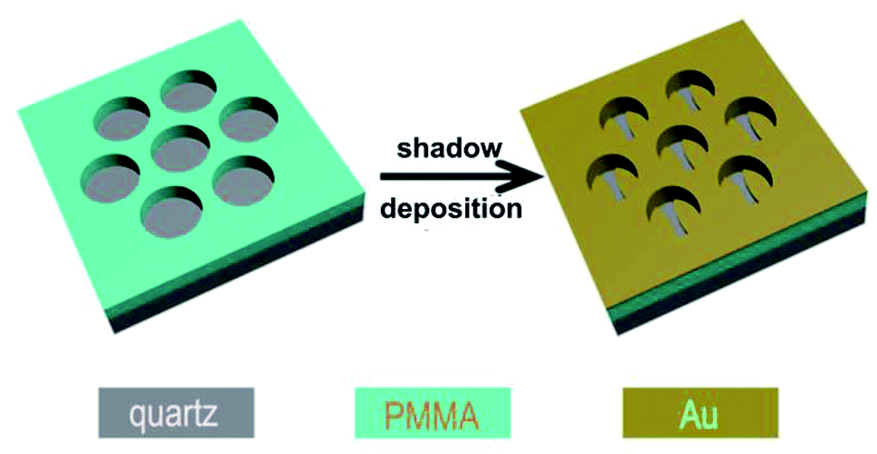 | ||
| Fig. 1 Schematic of fabricating spindles in nanowells. | ||
A gold spindle in a nanowell array was fabricated by a shadow deposition process. The size of spindles depends on the tilted angle of the shadow deposition. As revealed in Fig. 2, the average length of the spindles is 330 nm, 280 nm and 250 nm when the deposition angle is 30°, 45° and 60°, and the corresponding average width of the spindles is 135 nm, 120 nm and 80 nm (C) respectively. Clearly, the size of the spindles decreases with increasing the deposition angle from 30° to 60°. The spindles become smaller with the increase of the deposition angle. The roughness of the spindles should be introduced by the rough surface of nanowells, which is transferred from the mold (Fig. S2B†).
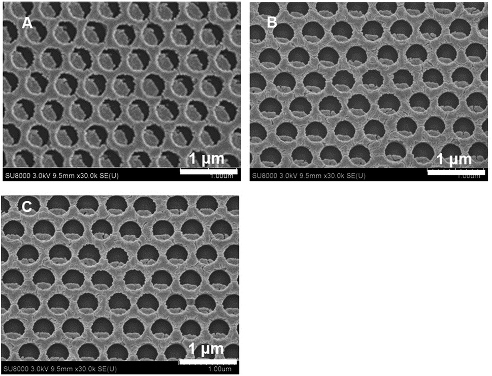 | ||
| Fig. 2 SEM images of one Au spindle in a nanowell array fabricated with tilted angle of (A) 30°, (B) 45°, and (C) 60°. | ||
Then the second shadow deposition was conducted after rotating the substrate for 180° along the axis to create the opposite spindles. In the first deposition process, the height of the nanowell was increased. The tilted angle of the second deposition was adjusted to obtain the same size spindles. The fabricated array was consisted of a metal nanomesh and two opposite Au spindles, which were connected along with the Au layer on the side wall, as shown in Fig. 3. Fig. 3A–C present the arrays created with the angle of 30°, 45°, and 60°, which are named as sample A, B and C respectively. The opposite spindles can be seen clearly in Fig. 3A and B. Dumbbell-shaped gaps are formed at the vacant areas without Au. The areas unable to deposit any Au in A and B are turned to dumbbell-shaped gaps. However, because of the large deposition angle, the morphology of the nanowell mask changes into ellipse and makes the bottom structures crescent moon like. The gaps turns spindle like. The average smallest width of the dumbbell-shaped gap is 75 nm, 100 nm and 150 nm respectively (detailed in Table S1†).
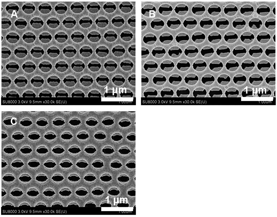 | ||
| Fig. 3 SEM images of the spindles created with the deposition angle of (A) 30°, (B) 45°, and (C) 60°. | ||
Through the results, we realize the limitation of our method. When the deposition angle is smaller than 60°, the size of the spindles can be tuned well. However, the morphology of the nanostructures cannot be tuned. Meanwhile, when the deposition angle is larger than 60°, the morphology of spindles is hard to maintain.
The reflection spectra of sample A in the range of 500 nm to 1100 nm collected under the polarized light parallel and perpendicular to the deposition axis are shown in Fig. 4A. When the polarized incident light is parallel to the axis, only a broad dip can be observed in the spectrum (black line). And when the incident light is perpendicular to the axis, a peak around 720 nm can be observed (red line). However, no peak or dip can be observed in the spectrum of PMMA nanowells (green line). The peak should be contributed by the spindles. To investigate the plasmonic sensing performance of the spindles in nanowells arrays, the reflection spectra of sample A in sucrose aqueous solutions of different concentrations are recorded and shown in Fig. 4B. The refractive index (RI) of the sucrose aqueous solution increases from 1.3330 to 1.4419 when the concentration changes from 0 to 60 wt%.9 Three pieces of sample A created individually were used to test the reproducibility. Fig. 4C shows that the wavelength shift against the RI fits well with the fitting curve.
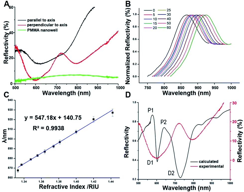 | ||
| Fig. 4 (A) Reflectivity of sample A. (B) Correlation of the reflectivity and the concentration of sucrose aqueous solution under the polarized light perpendicular to the axis. (C) Correlation of the wavelength and the RI. (D) Calculated and experimental reflectivity under polarized light perpendicular to the axis. | ||
Sensitivity (S) and figure of merit (FOM) are two main characteristics for evaluating the performance of plasmonic sensors. S can be calculated by:
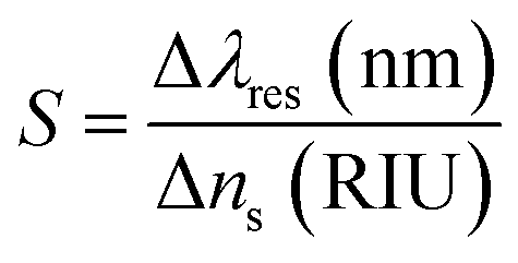 | (1) |
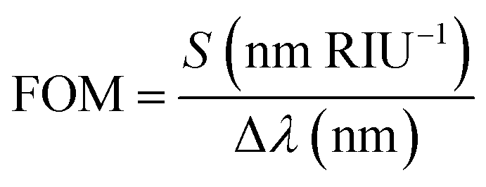 | (2) |
To further understanding the plasmonic property of the structure, a FDTD simulation was introduced. The distribution of electromagnetic field is given in Fig. S3† (line C), which indicates that this peak is contributed by the coupling of PSPR of the Au mesh and LSPR of the spindles.
Fig. 4D presents the calculated and experimental spectrum, which are similar in shape. However, there are deviations in the positions between the calculated and experimental spectra. It is the difference between the real structure and the model for calculation caused the deviation. It is difficult to build up a model exactly same as the real sample due to the following reasons. First, there are some defects in the arrangement for real sample; second, the surface of the nanomesh is rough; third, the thickness of Au along the side wall of nanowell varies. The results indicate that P1, D1 and D2 were caused by both PSPR and LSPR of the gold mesh (line A, B, D in Fig. S3†). P2, used for RI sensing, is introduced by the coupling of PSPR of the Au mesh and LSPR of the spindles (line C in Fig. S3†).
To test the SERS activity of this structure, we collected the SERS spectra using rhodamine 6G (R6G, 10−5 M) as a probe molecule, as displayed in Fig. 5A. The characteristic peaks of R6G molecules can be observed. The bonds at 610 cm−1 attribute to the out-of-plane C–C–C ring in-plane modes; 772 cm−1 attribute to the out-of-plane modes of ring; 1120 cm−1 attribute to in-plane C–H bending vibration mode; 1190, 1308, 1510, and 1572 cm−1 attribute to symmetric modes of in-plane C–C stretching vibrations; 1360 cm−1 and 1650 cm−1 are assigned to the aromatic C–C stretching. Taking the peak at 1650 cm−1 as reference, the Raman intensity decreases as the deposition angle increases. While the signal of Au nanowell array created by normal deposition shows the lowest intensity among them. We believe this was attributed to the bottom spindles. The side of spindles and the far field coupling of the two nanostructures provided electromagnetic field enhancement. As the distance increases, the coupling becomes weaker and provides lower electromagnetic field enhancement. With the smallest gap, the sample A shows the highest SERS activity. To find the detection limit of this structure for SERS measurements, we collected the SERS spectra of R6G molecule with concentrations from 10−5 M to 10−8 M on sample A, as shown in Fig. 5B. The Raman signal can be clearly observed when the concentration is down to 10−8 M. Based on the intensities of peaks at 1510 cm−1 and 1650 cm−1, the average calculated EF factors are 8.68 × 10⁻⁴ and 1.29 × 10⁻⁵ according to the formula reported elsewhere. To investigate the reproducibility, SERS spectra were collected on 10 randomly selected points, as shown in Fig. 5C. The RSD is calculated based on the intensities of peak at 1650 cm−1 (shown in Fig. 5D), which is 6.24%. The above results indicate that this kind of structures can be applied in SERS detection.
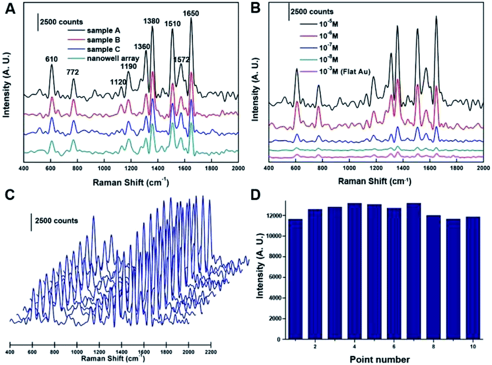 | ||
| Fig. 5 (A) SERS spectra of R6G (10−5 M) collected on the sample A, B, C and Au nanowell array fabricated under normal deposition. (B) SERS spectra of R6G (10−5 M to 10−8 M) collected on sample A and R6G (10−3 M) on flat Au surface. (C) SERS spectra of R6G (10−5 M) collected on 10 randomly points from sample A. (D) The Raman intensities at 1650 cm−1 in (C). | ||
Conclusions
In conclusion, we present a method to fabricate opposite metal spindles in nanowells array by two-step shadow deposition using the PMMA nanowell array as shadow mask. The dumbbell-shaped gap between a pair of spindles can be tuned by adjusting the deposition angle. The structure with gap size of 75 nm shows a high sensing sensitivity, which exhibits the 547.18 nm RIU−1 and an acceptable FOM of 7.27 RIU−1 for RI detection. A 3D-FDTD simulation reveals that the resonance peak was caused by the coupling of PSPR of the Au mesh and LSPR of the spindles. Furthermore, this kind of array shows good SERS activity with EF of 1.29 × 10⁵ and a RSD of 6.24%. This method may be utilized in the fabrication of structures for detecting and sensing fields.Acknowledgements
This work was supported by the National Natural Science Foundation of China (No. 20373019 and 21273092).Notes and references
- J. Park, Y. Choi, M. Lee, H. Jeon and S. Kim, Nanoscale, 2015, 7, 426–431 RSC.
- X. Zhang, Y. Zheng, X. Liu, W. Lu, J. Dai, D. Y. Lei and D. R. MacFarlane, Adv. Mater., 2015, 27, 1090–1096 CrossRef CAS PubMed.
- M. L. Juan, M. Righini and R. Quidant, Nat. Photonics, 2011, 5, 349–356 CrossRef CAS.
- J. N. Anker, W. P. Hall, O. Lyandres, N. C. Shah, J. Zhao and R. P. Van Duyne, Nat. Mater., 2008, 7, 442–453 CrossRef CAS PubMed.
- H. Im, K. C. Bantz, N. C. Lindquist, C. L. Haynes and S. H. Oh, Nano Lett., 2010, 10, 2231–2236 CrossRef CAS PubMed.
- W. Kubo and S. Fujikawa, Nano Lett., 2011, 11, 8–15 CrossRef CAS PubMed.
- M. Lee, H. Jeon and S. Kim, Nano Lett., 2015, 15, 3358–3363 CrossRef CAS PubMed.
- M. Najiminaini, F. Vasefi, B. Kaminska and J. J. L. Carson, Plasmonics, 2013, 8, 217–224 CrossRef CAS.
- F. Wu, L. Liu, L. Feng, D. Xu and N. Lu, Nanoscale, 2015, 7, 13026–13032 RSC.
- Y. Shen, J. Zhou, T. Liu, Y. Tao, R. Jiang, M. Liu, G. Xiao, J. Zhu, Z. K. Zhou, X. Wang, C. Jin and J. Wang, Nat. Commun., 2013, 4, 2381 Search PubMed.
- Y. Shen, X. Chen, Z. Dou, N. P. Johnson, Z. K. Zhou, X. Wang and C. Jin, Nanoscale, 2012, 4, 5576–5580 RSC.
- H. Duan, A. I. Fernandez-Dominguez, M. Bosman, S. A. Maier and J. K. Yang, Nano Lett., 2012, 12, 1683–1689 CrossRef CAS PubMed.
- G. F. Walsh and L. Dal Negro, Nano Lett., 2013, 13, 3111–3117 CrossRef CAS PubMed.
- H. Rochholz, N. Bocchio and M. Kreiter, New J. Phys., 2007, 9, 53 CrossRef.
- M. Swartz, M. Rodriguez, A. D. Quast, C. T. Cooper, S. Blair and J. S. Shumaker-Parry, J. Phys. Chem. C, 2016, 120, 20597–20603 CAS.
- L. Y. Wu, B. M. Ross and L. P. Lee, Nano Lett., 2009, 9, 1956–1961 CrossRef CAS PubMed.
- Z. B. Li, X. M. Zhang, S. S. Ye, J. N. Zhang, T. Q. Wang, L. P. Fang, J. H. Zhang and B. Yang, Nanotechnology, 2013, 24, 105307 CrossRef PubMed.
- J. Zhao, C. Zhang, P. V. Braun and H. Giessen, Adv. Mater., 2012, 24, OP247–252 CrossRef CAS PubMed.
- N. Vogel, J. Fischer, R. Mohammadi, M. Retsch, H. J. Butt, K. Landfester, C. K. Weiss and M. Kreiter, Nano Lett., 2011, 11, 446–454 CrossRef CAS PubMed.
- T. Liu, Y. Shen, W. Shin, Q. Zhu, S. Fan and C. Jin, Nano Lett., 2014, 14, 3848–3854 CrossRef CAS PubMed.
- M. Zhang, N. Large, A. L. Koh, Y. Cao, A. Manjavacas, R. Sinclair, P. Nordlander and S. X. Wang, ACS Nano, 2015, 9, 9331–9339 CrossRef CAS PubMed.
- Y. S. Jung, Z. Sun, H. K. Kim and J. Blachere, Appl. Phys. Lett., 2005, 87, 263116 CrossRef.
- T. Kolb, F. Kost, F. Neubrech, M. E. Toimil-Molares, T. Cornelius, R. Neumann, A. Pucci and G. Fahsold, Infrared Phys. Technol., 2006, 49, 29–34 CAS.
- Y. Choi, S. Hong and L. P. Lee, Nano Lett., 2009, 9, 3726–3731 CrossRef CAS PubMed.
- A. Lesuffleur, H. Im, N. C. Lindquist and S.-H. Oh, Appl. Phys. Lett., 2007, 90, 243110 CrossRef.
Footnote |
| † Electronic supplementary information (ESI) available: Detailed experimental section; scheme of fabricating process of the NIL mold; SEM of the NIL mold and PMMA nanowells; the detailed parameter of samples; distribution of EF of sample A. See DOI: 10.1039/c6ra25332f |
| This journal is © The Royal Society of Chemistry 2017 |