
 Open Access Article
 This Open Access Article is licensed under a
 Creative Commons Attribution 3.0 Unported Licence
Tuning optical band gap by electrochemical reduction in TiO2 nanorods for improving photocatalytic activities†
Jong-Won Yun a,
Ki Yeon Ryua,
Tri Khoa Nguyena,
Farman Ullaha,
Yun Chang Parkb and
Yong Soo Kim*a
a,
Ki Yeon Ryua,
Tri Khoa Nguyena,
Farman Ullaha,
Yun Chang Parkb and
Yong Soo Kim*a
aDepartment of Physics, Energy Harvest-Storage Research Center, University of Ulsan, Ulsan 44610, South Korea. E-mail: yskim2@ulsan.ac.kr
bMeasurement and Analysis Division, National Nanofab Center, Daejeon 34141, South Korea
First published on 18th January 2017
Abstract
In this study, we investigate the tuning of the optical band gap of TiO2 nanorods (TiO2 NRs) by electrochemical methods for improving their photocatalytic activities. A seed layer prepared by RF-magnetron sputtering is employed to increase the adhesion between TiO2 NRs and substrate to prevent the peel-off of TiO2 NRs from substrate during electrochemical reduction process. The morphological study shows the stability of TiO2 NRs structure after reduction process. The electrochemical reduction process increased the amount of Ti3+ (a reduced state of Ti4+) and oxygen vacancy by 2.2% and 3.6%, respectively. The process also tune the optical band of TiO2 NRs from 3.0 eV to 2.84 eV due to the up-shift of valence band to Fermi level. The reduced band gap of NRs improve the photocatalytic activities by 1.48 times due the increase of its absorbance range from UV to visible in solar spectrum. The photocatalytic activities were 24.3 times improved by depositing a ultrathin layer of Pt as electron collector.
Introduction
Its excellent chemical stability, nontoxicity, catalytic activity and low cost make TiO2 an attractive photocatalytic material for a range of applications, such as water purification, self-cleaning, and solar energy conversion.1–4 On the other hand, the use of TiO2 in the visible region is limited by its large energy band gap. In recent years, significant effort has been devoted to improving the visible absorbance of TiO2 to enhance its photocatalytic activity in solar light.5–19A well-known approach is hetero-doped TiO2 using impurity cations, Cr, Ag, etc., and anions, N, F, C, etc.6,9–12 Nitrogen-doped TiO2 may produce sub-levels by hybridization of the N 2p and O 2p states near the valence band of TiO2 that would improve the visible light activity.12 On the other hand, it can produce carrier recombination centers that may reduce the catalytic activity in the UV region.20–23 Self-doped TiO2 is a useful method for improving the photocatalytic activities of TiO2 in the UV-Vis region by generating a sub-band level in the TiO2 band gap and not involving structure defects.24–29 Naldoni et al. reported that the reduced band gap of Ti3+ self-doped TiO2 results from the slight up-shift of the valence band (VB) to the Fermi level.21 Kang et al. also reported the same behavior of the up-shift of VB.30 Moreover, the oxygen vacancies (VO) formed during Ti3+ self-doping increase the carrier density and charge transfer.31 Well-known approach could be the thermal annealing method used famously for Ti3+ self-doped TiO2;32–36 however, it require a carrier gas and control system for temperature and pressure. Recently, an electrochemical reduction method has been adopted widely because of its simple mechanism, low cost and fast self-doping properties. On the other hand, owing to the lattice mismatch between rutile TiO2 and the substrate,37 electrochemical self-doped approach is only employed in TiO2 nanotubes anodized from Ti-foil.30,38–40
In this study, the electrochemical reduction method was used to self-dope Ti3+ into TiO2 nanorods (TiO2 NRs) grown on a FTO substrate for optical band gap tuning. To prevent the peel-off of TiO2 NRs from the substrate due to large lattice mismatch, a TiO2 seed layer was introduced by RF-magnetron sputtering to enhance the adhesion between TiO2 and FTO substrate. X-ray photoelectron spectroscopy and UV-Vis spectroscopy were employed to examine the tuning of the TiO2 optical band gap. In a study of photocatalysis, the reduced TiO2 nanorods (rTiO2 NRs) exhibited better performance compared to the as-grown TiO2 NRs. The photocatalytic activities of rTiO2 NRs were enhanced significantly by decorating an ultrathin layer of Pt on the rTiO2 NRs as an electron collector by RF magnetron sputtering.
Experiment
Synthesis of TiO2 nanorods
Prior to synthesis, FTO substrate (F:SnO2, Tec 20, 8 Ω □−1) was cleaned by immersing in a mixture of DI water, acetone and 2-propanol (1![[thin space (1/6-em)]](https://www.rsc.org/images/entities/char_2009.gif) :1:1 of volume ratio) and ultra-sonicated for 30 min. TiO2 seed layer was deposited on FTO substrate using RF-magnetron sputtering (details in Table S1†). To synthesize TiO2 NRs by hydrothermal method, 0.65 mL of titanium(IV) n-butoxide (TBO, Aldrich Chemicals, 97%), 25 mL of HCl 38%, and 25 mL of DI water were mixed and stirred for 30 min.
:1:1 of volume ratio) and ultra-sonicated for 30 min. TiO2 seed layer was deposited on FTO substrate using RF-magnetron sputtering (details in Table S1†). To synthesize TiO2 NRs by hydrothermal method, 0.65 mL of titanium(IV) n-butoxide (TBO, Aldrich Chemicals, 97%), 25 mL of HCl 38%, and 25 mL of DI water were mixed and stirred for 30 min.
RF-deposited TiO2 seed layer on FTO substrate was placed face side down in the grown solution in a Teflon beaker. To grow the TiO2 NRs, the Teflon beaker was then sealed in a stainless steel auto-clave at 165 °C for 10 h. The as-grown TiO2 NRs were washed with DI water and ethanol, and then annealed at 450 °C for 60 min. To compare the quality of RF-sputtered seed layer, another TiO2 NRs were also grown on a seed layer prepared by sol–gel method. The seed layer was prepared by spin coating of TiO2 polymeric solution.41,42
Electrochemical reduction of TiO2 NRs and Pt decoration
The synthesized TiO2 NRs were reduced using an electrochemical reduction method; connecting TiO2 NRs/FTO (working electrode) and a Pt wire (counter electrode, 1 mm of diameter and 9 cm of length, 99.95%). Electrochemical reduction process was done in a 0.1 M of NaOH electrolyte with negative bias, −3 V vs. Pt for 5 to 20 min. The final rTiO2 NRs were washed in DI water, and dried with dry N2. To improve photocatalytic activities, an ultrathin layer of Pt as electron collector was deposited on surface of the rTiO2 NRs by using a RF-magnetron sputtering at 30 W for 2 min (details in Table S1†).Characterization
The morphology and crystallinity of the TiO2 NRs and rTiO2 NRs were studied using field emission scanning electron microscopy (FE-SEM, JEOL, JSM 7600F) and a transmission electron microscope (FE-TEM, JEI, Tecnai G2F30 S-Twin). The crystalline structure was characterized by a X-ray diffraction (XRD, RIGAKU, D/MAX 2500-V/PC, using Cu Kα radiation, λ = 1.540598 Å). X-ray photoelectron spectroscopy (XPS) using a Leybold spectrometer with an Al Kα monochromatic beam (1486.6 eV, ESCALAB250, Theta Probe XPS system) and ultra-violet photoelectron spectroscopy (UPS) study with a He(I) beam source (21.21 eV) was done. UV-Vis spectra were recorded using an optical spectrophotometer (Varian, Cary 5000).Photocatalytic activities measurement
Photocatalytic performances of the TiO2 NRs, rTiO2 NRs and Pt decorated rTO2 NRs were evaluated by photo-degradation of 15 mL of 15 μM methylene blue (MB, C16H18N3SCl) under Xe-lamp irradiation. The intensity of the light source was calibrated with a standard Si-photodiode detector of a KG-3 filter (Newport Co., Oriel) to AM 1.5G illumination of 100 mW cm−2. Photocatalytic degradation of MB was determined from the absorbance of MB solution at 665 nm using a UV-Vis spectrophotometer.Results and discussion
Fig. 1(a) shows schematically the growth process of TiO2 NRs, rTiO2 NRs and Pt decorated rTiO2 NRs on a RF-magnetron sputtered TiO2 seed layer/FTO substrate. The RF-sputtered TiO2 seed layer plays an important role in enhancing the adhesion between the grown TiO2 NRs and substrate. The insets in Fig. 1(b) and (c) show photographs of the TiO2 NRs before and after reduction, respectively. The TiO2 NRs has maintained their quality, indicating the good adhesion between the TiO2 NRs and substrate. On the other hand, the rTiO2 NRs on sol–gel TiO2 seed layer show poor adhesion as compared to those on the RF-magnetron sputtered seed layer (Fig. S1†). Moreover, the RF-sputtered seed layer exhibited higher mechanical durability as compared to sol–gel.43,44 To check the adhesion more closely, the sample was analyzed by FE-SEM before and after the reduction process, as depicted in Fig. 1(b) and (c), respectively. The TiO2 NRs preserved their quality, which further confirmed the excellent adhesion between TiO2 NRs and substrate. | ||
| Fig. 1 (a) Schematic diagram of experimental sequence. (b and c) FE-SEM images of (b) TiO2 NRs and (c) rTiO2 NRs (insets: photograph image of (b) TiO2 NRs and (c) rTiO2 NRs on FTO substrate, indicating that the TiO2 NRs was changed from white to dark brown after the reducing process while the morphology was stable). (d) TEM (inset: a low-magnification image) and (e) HR-TEM image of TiO2 NRs grown along the [001] direction with an average length of 1.5 μm and diameter of 65 nm. (f) XRD result of TiO2 NRs and rTiO2 NRs. Two peaks are appeared at 30.64° and 31.96° 2θ after electrochemical reduction by the formation of VO. (g) TEM image and (h–k) EDS mapping images of the ultrathin Pt decorated rTiO2 NRs. The inset in (h) shows Pt decorated rTiO2 NRs used EDS mapping. | ||
The TEM image in Fig. 1(d) shows that the TiO2 NRs are approximately 1.5 μm in length and 65 nm in diameter. The HR-TEM image shown in Fig. 1(e) taken at the highlighted region in Fig. 1(d) shows that the growth direction of TiO2 NR is along the (001) direction, which confirms the typical TiO2 NR structure. This observation is similar to previous reports.45 Fig. 1(f) show the XRD results of the TiO2 NRs and rTiO2 NRs. The diffraction peaks at 26.42°, 33.68°, 37.68°, 51.46°, 61.54° and 65.46° 2θ (gray circles) correspond to the crystalline structure of the FTO substrate (S.G. P42/mnm, JCPDS no. 00-046-1088, a = b = 0.4750 nm, c = 0.3198 nm). The XRD peaks at 36.04°, 41.22°, 54.30°, 62.70° and 68.92° 2θ (dark squares) are consistent with the tetragonal rutile phase of TiO2 (S.G. P42/mnm, JCPDS no. 01-070-7347, a = b = 0.4593 nm and c = 0.2961 nm).46 The rutile structure has a 42 screw axis along the c-axis; hence, the domination of (110) faces indicates the promoted growth of the TiO2 NR along the (001) direction.47–49 After electrochemical reduction, two XRD peaks (red diamonds) are appeared at 30.64° and 31.96° 2θ which match to the (![[2 with combining macron]](https://www.rsc.org/images/entities/char_0032_0304.gif) 03) and
03) and  faces of Ti4O7 (S.G. P1, JCPDS no. 77-1390) lacking oxygen atoms. This shows that the electrochemical process is suitable for generating oxygen vacancies (VO) in rTiO2 NRs. Owing to the lower band gap of rTiO2 NRs as compared to the TiO2 NRs, the rTiO2 NRs can perform better photocatalytic behavior in UV-Vis irradiation.
On the other hand, the charge recombination can affect the rTiO2 NRs performance. Therefore, to avoid the recombination of photo-generated electron–hole pairs, an ultrathin layer of Pt was deposited on the rTiO2 NRs by RF-magnetron sputtering. The Pt distribution on rTiO2 NRs was analysed HR-TEM, as shown in Fig. 1(g) and S2.† It shows that amorphous Pt is uniformly decorated on rTiO2 NRs surface with the average width and thickness are about 2.2 and 3.4 nm, respectively. Energy-dispersive X-ray spectroscopy (EDS) elementary mapping images in Fig. 1(h)–(k) show the excellent coated (almost conformal) of Pt on whole interface of exposed rTiO2 NRs.
The sample was further characterized by XPS to examine the effect of the reduction process on atomic bonding in the TiO2 NRs. The Ti 2p3/2 spectra before and after reduction are given in Fig. 2(a). The figure shows a weak peak at 456.9 eV and a strong peak at 458.3 eV, corresponding to Ti3+ and Ti4+, respectively. The intensity of the Ti3+ peak increased after the reduction process, which indicates the reduction of TiO2. The total increase was found to be 2.2%. Moreover, the change in the relative intensity of Ti3+ indicates the self-doping of Ti3+ into TiO2 NRs.39,50,51 The O 1s survey in Fig. 2(b) shows the presence of oxygen vacancies (VO) at 531.0 eV, strong binding of crystalline Ti–O in TiO2 at 529.5 eV, and weak binding of Ti and oxygen at the TiO2 surface at 527.8 eV.50,51 The intensity of VO increased by 3.6% after the reduction process.
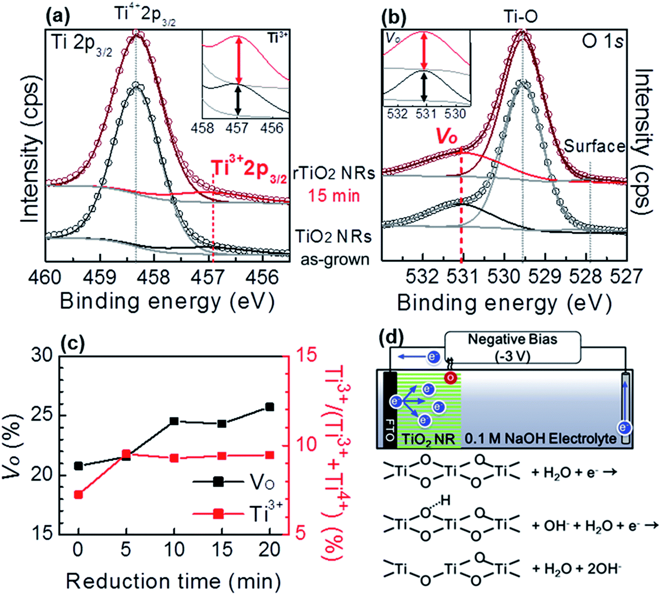 | ||
| Fig. 2 XPS core levels spectra of (a) Ti 2p3/2 and (b) O 1s of TiO2 NRs and rTiO2 NRs (inset: magnification graph of (a) Ti3+ peak and (b) VO peak). (c) Time dependent proportion change of VO and Ti3+ obtained from deconvolution of XPS results. Ti3+ content is likely to saturate at a mean value of 9.4% after 5 min of reduction time, VO defect increase linearly with reduction time. (d) Schematic description of electrochemical reduction process. The reaction of surface oxygen with water generates VO (O–Ti4+–VO) and electrons supported from counter electrode could inject to Ti4+ to form Ti3+. | ||
Fig. 2(c) shows the reduction time dependent formation of Ti3+ and VO in rTiO2 NRs, which was calculated from XPS data deconvolution shown in Fig. S3.† The Ti3+ was found to be saturated at an average 9.4% after a 5 min reduction time, while the VO defects is found to be saturated at about 24% after 10 min of reduction time. This phenomenon can be explained by a reduction mechanism shown schematically in Fig. 2(d). Electrons supported from the counter electrode could inject into Ti4+ to form Ti3+. The larger amount of electron injected into Ti4+ may rapidly reduce it to Ti3+ (saturated after 5 min reduction). Thus, the bonding of oxygen and Ti3+ is weaken then oxygen atoms at surface react with hydrogen ions (H+, separated from water) to generate oxygen vacancies.
The VB position of the TiO2 NRs and rTiO2 NRs were analyzed from the VB XPS spectra, as shown in Fig. 3(a). The VB edge of TiO2 NRs and rTiO2 NRs observed at 2.25 eV and 2.09 eV, respectively, under the Fermi level, which indicates that the VB edge of the rTiO2 NRs was shifted 0.16 eV to the Fermi level.21,30 The same behavior can be observed in plots of the Kubelka–Munk function vs. the photon energy transformed from the total diffuse transmittance (Fig. S4†) shown in Fig. 3(b). The TiO2 NRs reveal a band gap of 3.0 eV,52 whereas the rTiO2 NRs exhibit an optical band gap of 2.84 eV, which is 0.16 eV lower. Fig. 3(c) shows work-function deduced from UPS spectra before and after the electrochemical reduction of TiO2 NRs. Gap between CB and Fermi level was maintained, while the Fermi level of rTiO2 NRs was raised 0.78 eV after reduction, as shown in Fig. 3(d). Therefore, reduced optical band gap of rTiO2 NRs is attributed to up-shifting of VB. Every result in the UV-Vis transmittance and XPS (UPS) analysis are in well agreement. These results confirm that the surface defect in the rTiO2 NRs reduce its optical band-gap by up-shifting the VB edge, which is in good agreement with previous reports.21,30,38,51 Fig. 3(e) and S5† presents the time evolution of the VB and the tuning of the optical band gap with respect to the reduction time. Both of VB position and band gap of rTiO2 NRs are found to be saturated at about 2.1 and 2.85 eV, respectively, after 10 min of reduction time. The modification of the optical band gap of the rTiO2 NRs is similar to the shifted value of the VB edge to the Fermi level for all reduction times. Therefore, the reduction of the optical band-gap of rTiO2 NRs by the electrochemical reduction was attributed to the modification of the VB edge.21,30,39,53
 | ||
| Fig. 3 (a) VB position analyzed from VB XPS spectra, (b) plots of Kubelka–Munk function vs. the photon energy and (c) work-function analyzed from UPS spectra of TiO2 NRs and rTiO2 NRs. (d) Schematic description of band structure of TiO2 NRs before and after reduction. (e) Evolution of valence band and optical band gap with respect to the reduction time. After reduction for 15 min, the Fermi level was raised 0.78 eV and the VB edge is shifted up 0.16 eV to the Fermi level. The modification of the optical band gap is similar to that the VB edge. | ||
Fig. 4 shows the photocatalytic activities of the samples evaluated by the photo-degradation of methylene blue (M.B.) in an aqueous solution. As shown in Fig. 4(a) and S6(a),† the rTiO2 NRs and Pt/rTiO2 NRs show 1.48 and 12.85 times higher photocatalytic activities than that of the TiO2 NRs and Pt/TiO2 NRs under UV-Vis irradiation in a 180 min and 90 min reaction, respectively. This effect can be attributed to the reduction of the optical band gap. For further improvement, an ultrathin layer of Pt was deposited by RF-magnetron sputtering, as shown in Fig. 1(g). The ultrathin Pt layer can act as an electron collector, thereby reducing the charge recombination of the photo-generated electron/hole pair (e–h pair). This can enhance the overall performance. The photocatalytic activities of the Pt decorated rTiO2 NRs are given in Fig. 4 and S6.† This shows that the photocatalytic activities and reaction rate constant k of Pt/rTiO2 NRs (98.2% of M.B. degradation in 90 min, k = 0.038 min−1) increased 24.3 and 9.5 fold compared with the rTiO2 NRs (31.2% of M.B. degradation in 90 min, k = 0.004 min−1).
 | ||
| Fig. 4 (a) Photo-degradation of M.B. in TiO2 NRs, rTiO2 NRs, Pt decorated TiO2 NRs (Pt/TiO2 NRs) and Pt decorated rTiO2 NRs (Pt/rTiO2 NRs). The photocatalytic activities are enhanced after electrochemical reduction and decoration of Pt, due to the reduction of the optical band gap and recombination, respectively. (b) Photocatalytic performance of Pt decorated rTiO2 NRs with different reduction times. (c) Recycled photocatalytic activities of Pt decorated rTiO2 NRs. (d) Schematic description of the photocatalytic activities of Pt decorated rTiO2 NRs. | ||
Furthermore, the Pt-decorated rTiO2 NRs also has substantial stability and cyclic endurance of the photocatalytic activities by the excellent photo-degradation of M.B. for 8 cycles, shown in Fig. 4(c). Fig. 4(b) and S6(b)† shows the photocatalytic performance of the Pt/rTiO2 NRs with different electro-chemical reduction time. The results reveal that photocatalytic activities of rTiO2 NRs were saturated after 10 min of reduction time. The photocatalytic behavior is in good agreement with the band structure results shown in Fig. 3(c). The rate constant k for 3 samples of 10, 15 and 20 min of reduction time are found to be similar (from 0.030 to 0.038 min−1). A further reduction of the optical band gap resulted in further improvement of the photocatalytic activities.
Fig. 4(d) presents the mechanism of the enhanced photocatalytic activities of the Pt decorated rTiO2 NRs. The conduction band (CB) of rTiO2 NRs is located at approximately −4.4 eV under vacuum level, while the Fermi level of Pt is located under the CB of the rTiO2 NRs.54–56 Owing to the narrower band gap, the rTiO2 NRs can absorb UV to blue light in the solar spectrum to generate e–h pairs. The photo-excited electrons from rTiO2 NRs tend to transfer to Pt. The ultrathin Pt collects the electrons and improves charge transfer efficiency. The photo-excited electrons trapped on Pt react with oxygen to form superoxide radicals or hydroperoxide radical to degrade M.B. The photo-excited holes located in the rTiO2 NRs oxidize water to produce hydroxyl radical to oxide M.B.57,58
Conclusions
This study examined the optical band gap tuning of TiO2 NRs by an electrochemical reduction method and its effects on the photocatalytic activities. The reduction process tune the optical band gap from 3.0 eV to 2.84 eV, enabling TiO2 NRs to absorb UV to the blue light frequencies in the solar spectrum. This reduction in band gap enhanced its photocatalytic activity 1.48 fold. In addition, Pt, as an electron collector layer, was found to be another important parameter. The ultrathin Pt layer greatly reduces the e–h recombination process and can improve the photocatalytic activity significantly (24.3 fold). Moreover, the RF-magnetron sputtered TiO2 seed layer showed much better adhesion properties than the seed layer prepared by the sol–gel method.Acknowledgements
This research was supported by the Priority Research Centers Program (2009-0093818), the Basic Science Research Program (2015R1D1A3A03019609), and the Basic Research Lab Program (2014R1A4A1071686) through the National Research Foundation of Korea (NRF), funded by the Korean Government. This research was also supported by the “Leaders Industry-University Cooperation” Project, supported by the Ministry of Education (MOE). Y. S. Kim also thanks to Prof. S. Park and Mr J.-W. Kim of the Dep. of Physics, Pusan National University and Dr J.-S. Bae of Busan center, Korea Science Institute for the XPS analysis.Notes and references
- Z. Gan, X. Wu, M. Meng, X. Zhu, L. Yang and P. K. Chu, ACS Nano, 2014, 8, 9304–9310 CrossRef CAS PubMed.
- A. Fakharuddin, F. D. Giacomo, A. L. Palma, F. Matteocci, I. Ahmed, S. Razza, A. D'Epifanio, S. Licoccia, J. Ismail, A. D. Carlo, T. M. Brown and R. Jose, ACS Nano, 2015, 9, 8420–8429 CrossRef CAS PubMed.
- Y. Dou, S. Zhang, T. Pan, S. Xu, A. Zhou, M. Pu, H. Yan, J. Han, M. Wei, D. G. Evans and X. Duan, Adv. Funct. Mater., 2015, 25, 2243–2249 CrossRef CAS.
- B. Qiu, M. Xing and J. Zhang, J. Am. Chem. Soc., 2014, 136, 5852–5855 CrossRef CAS PubMed.
- J.-Y. Zheng, S.-H. Bao, Y. Guo and P. Jin, ACS Appl. Mater. Interfaces, 2014, 6, 5940–5946 CAS.
- J. Tao, M. Yang, J. W. Chai, J. S. Pan, Y. P. Feng and S. J. Wang, J. Phys. Chem. C, 2014, 118, 994–1000 CAS.
- Z. Zhan, J. An, H. Zhang, R. V. Hansen and L. Zheng, ACS Appl. Mater. Interfaces, 2014, 6, 1139–1144 CAS.
- I. S. Cho, M. Logar, C. H. Lee, L. Cai, F. B. Prinz and X. Zheng, Nano Lett., 2014, 14, 24–31 CrossRef CAS PubMed.
- S. N. R. Inturi, T. Boningari, M. Suidan and P. G. Smirniotis, J. Phys. Chem. C, 2014, 118, 231–242 CAS.
- S. Padikkaparambil, Z. Yaakob, B. N. Narayanan, R. Ramakrishnan and S. Viswanathan, J. Sol-Gel Sci. Technol., 2012, 63, 108–115 CrossRef CAS.
- J. Biedrzycki, S. Livraghi, E. Giamello, S. Agnoli and G. Granozzi, J. Phys. Chem. C, 2014, 118, 8462–8473 CAS.
- R. Asahi, T. Morikawa, T. Ohwaki, K. Aoki and Y. Taga, Science, 2001, 293, 269–271 CrossRef CAS PubMed.
- A. Kumar and T. Mohanty, J. Phys. Chem. C, 2014, 118, 7130–7138 CAS.
- R. Asahi, T. Morikawa, H. Irie and T. Ohwaki, Chem. Rev., 2014, 114, 9824–9852 CrossRef CAS PubMed.
- Z. Jiang, Y. Tang, Q. Tay, Y. Zhang, O. I. Malyi, D. Wang, J. Deng, Y. Lai, H. Zhou, X. Chen, Z. Dong and Z. Chen, Adv. Energy Mater., 2013, 3, 1368–1380 CrossRef CAS.
- M.-Z. Ge, C.-Y. Cao, S.-H. Li, Y.-X. Tang, L.-N. Wang, N. Qi, J.-Y. Huang, K.-Q. Zhang, S. S. Al-Deyabe and Y.-K. Lai, Nanoscale, 2016, 8, 5226–5234 RSC.
- Y.-C. Pu, G. Wang, K.-D. Chang, Y. Ling, Y.-K. Lin, B. C. Fitzmorris, C.-M. Liu, X. Lu, Y. Tong, J. Z. Zhang, Y.-J. Hsu and Y. Li, Nano Lett., 2013, 13, 3817–3823 CrossRef CAS PubMed.
- Y. Tang, Z. Jiang, G. Xing, A. Li, P. D. Kanhere, Y. Zhang, T. C. Sum, S. Li, X. Chen, Z. Dong and Z. Chen, Adv. Funct. Mater., 2013, 23, 2932–2940 CrossRef CAS.
- M. Ge, Q. Li, C. Cao, J. Huang, S. Li, S. Zhang, Z. Chen, K. Zhang, S. S. Al-Deyab and Y. Lai, Adv. Sci., 2016, 3, 1600152 Search PubMed.
- S. Liu, J. Yu and W. Wang, Phys. Chem. Chem. Phys., 2010, 12, 12308–12315 RSC.
- A. Naldoni, M. Allieta, S. Santangelo, M. Marelli, F. Fabbri, S. Cappelli, C. L. Bianchi, R. Psaro and V. D. Santo, J. Am. Chem. Soc., 2012, 134, 7600–7603 CrossRef CAS PubMed.
- G. R. Torres, T. Lindgren, J. Lu, C.-G. Granqvist and S.-E. Lindquist, J. Phys. Chem. B, 2004, 108, 5995–6003 CrossRef CAS.
- J. Wang, D. N. Tafen, J. P. Lewis, Z. Hong, A. Manivannan, M. Zhi, M. Li and N. Wu, J. Am. Chem. Soc., 2009, 131, 12290–12297 CrossRef CAS PubMed.
- X. Chen, L. Liu and F. Huang, Chem. Soc. Rev., 2015, 44, 1861–1885 RSC.
- Z. Zhang, X. Yang, M. N. Hedhili, E. Ahmed†, L. Shi and P. Wang, ACS Appl. Mater. Interfaces, 2014, 6, 691–696 CAS.
- J. Chen, W. Song, H. Hou, Y. Zhang, M. Jing, X. Jia and X. Ji, Adv. Funct. Mater., 2015, 25, 6793–6801 CrossRef CAS.
- H. Zhou and Y. Zhang, J. Phys. Chem. C, 2014, 118, 5626–5636 CAS.
- B. Qiu, Y. Zhou, Y. Ma, X. Yang, W. Sheng, M. Xing and J. Zhang, Sci. Rep., 2015, 5, 8591 CrossRef CAS PubMed.
- F. Zuo, L. Wang, T. Wu, Z. Zhang, D. Borchardt and P. Feng, J. Am. Chem. Soc., 2010, 132, 1856–11857 Search PubMed.
- Q. Kang, J. Cao, Y. Zhang, L. Liu, H. Xu and J. Ye, J. Mater. Chem. A, 2013, 1, 5766–5774 CAS.
- J. M. Macak, B. G. Gong, M. Hueppe and P. Schmuki, Adv. Mater., 2007, 19, 3027–3031 CrossRef CAS.
- X. Chen, L. Liu, P. Y. Yu and S. S. Mao, Science, 2011, 331, 746–750 CrossRef CAS PubMed.
- J. E. Rekoske and M. A. Barteau, J. Phys. Chem. B, 1997, 101, 1113–1124 CrossRef CAS.
- J.-Y. Shin, J. H. Joo, D. Samuelis and J. Maier, Chem. Mater., 2012, 24, 543–551 CrossRef CAS.
- H. He, K. Yang, N. Wang, F. Luo and H. Chen, J. Appl. Phys., 2013, 114, 213505 CrossRef.
- S.-T. Myung, M. Kikuchi, C. S. Yoon, H. Yashiro, S.-J. Kim, Y.-K. Sun and B. Scrosati, Energy Environ. Sci., 2013, 6, 2609–2614 CAS.
- B. Liu and E. S. Aydil, J. Am. Chem. Soc., 2009, 131, 3985–3990 CrossRef CAS PubMed.
- C. Xu, Y. Song, L. Lu, C. Cheng, D. Liu, X. Fang, X. Chen, X. Zhu and D. Li, Nanoscale Res. Lett., 2013, 8, 391 CrossRef PubMed.
- Z. Zhang, M. N. Hedhili, H. Zhu and P. Wang, Phys. Chem. Chem. Phys., 2013, 15, 15637–15644 RSC.
- H. Li, Z. Chen, C. K. Tsang, Z. Li, X. Ran, C. Lee, B. Nie, L. Zheng, T. Hung, J. Lu, B. Pan and Y. Y. Li, J. Mater. Chem. A, 2014, 2, 229–236 CAS.
- X. Feng, K. Zhu, J. Frank, C. A. Grimes and T. E. Mallouk, Angew. Chem., 2012, 124, 2781–2784 CrossRef.
- H. S. Jung, J.-K. Lee, J. Lee, B. S. Kang, Q. Jia, M. Nastasi, J. H. Noh, C.-M. Cho and S. H. Yoon, Langmuir, 2008, 24, 2695–2698 CrossRef CAS PubMed.
- S. Takedaa, S. Suzukia, H. Odakaa and H. Hosonob, Thin Solid Films, 2001, 392, 338–344 CrossRef.
- M. Yamagishi, S. Kuriki, P. K. Song and Y. Shigesato, Thin Solid Films, 2003, 442, 227–231 CrossRef CAS.
- I. S. Cho, Z. Chen, A. J. Forman, D. R. Kim, P. M. Rao, T. F. Jaramillo and X. Zheng, Nano Lett., 2011, 11, 4978–4984 CrossRef CAS PubMed.
- P. Ballirano and R. Caminiti, J. Appl. Crystallogr., 2001, 34, 757–762 CrossRef CAS.
- W. J. Howard, Crystal Chemistry and Refractivity, Cambridge University, Cambridge, UK, 1988 Search PubMed.
- P. B. Allen, Nano Lett., 2007, 7, 6–10 CrossRef CAS PubMed.
- A. Kumar, A. R. Madaria and C. Zhou, J. Phys. Chem. C, 2010, 114, 7787–7792 CAS.
- B. Santara, P. K. Giri, K. Imakita and M. Fujii, J. Phys. Chem. C, 2013, 117, 23402–23411 CAS.
- M. C. Biesinger, L. W. M. Lau, A. R. Gerson and R. S. C. Smart, Appl. Surf. Sci., 2010, 257, 887–898 CrossRef CAS.
- J.-J. Wu and C.-C. Yu, J. Phys. Chem. B, 2004, 108, 3377–3379 CrossRef CAS.
- X. Chen, L. Liu, P. Y. Yu and S. S. Mao, Science, 2011, 331, 746–750 CrossRef CAS PubMed.
- W.-N. Wang, W.-J. An, B. Ramalingam, S. Mukherjee, D. M. Niedzwiedzki, S. Gangopadhyay and P. Biswas, J. Am. Chem. Soc., 2012, 134, 11276–11281 CrossRef CAS PubMed.
- H. Chen, S. Chen, X. Quan, H. Yu, H. Zhao and Y. Zhang, J. Phys. Chem. C, 2008, 112, 9285–9290 CAS.
- Y.-C. Chen, Y.-C. Pu and Y.-J. Hsu, J. Phys. Chem. C, 2012, 116, 2967–2975 CAS.
- S. Lakshmi, R. Renganathan and S. Fujita, J. Photochem. Photobiol., A, 1995, 88, 163–167 CrossRef CAS.
- A. Houas, H. Lachheb, M. Ksibi, E. Elaloui, C. Guillard and J.-M. Herrmann, Appl. Catal., B, 2001, 31, 145–157 CrossRef CAS.
Footnote |
| † Electronic supplementary information (ESI) available. See DOI: 10.1039/c6ra25274e |
| This journal is © The Royal Society of Chemistry 2017 |