
 Open Access Article
 This Open Access Article is licensed under a
 Creative Commons Attribution 3.0 Unported Licence
Piezoelectric energy harvesting from a PMN–PT single nanowire†
Brindha Moorthy‡
a,
Changyeon Baek‡a,
Ji Eun Wang a,
Chang Kyu Jeongab,
San Moona,
Kwi-Il Park*c and
Do Kyung Kim*a
a,
Chang Kyu Jeongab,
San Moona,
Kwi-Il Park*c and
Do Kyung Kim*a
aDepartment of Materials Science and Engineering, Korea Advanced Institute of Science and Technology (KAIST), 291 Daehak-ro, Yuseong-gu, Daejeon 34141, Republic of Korea. E-mail: dkkim@kaist.ac.kr; Fax: +82-42-350-3310; Tel: +82-42-350-4118
bKAIST Institute for the NanoCentury (KINC), 291 Daehak-ro, Yuseong-gu, Daejeon, 34141, Republic of Korea
cDepartment of Energy Engineering, Gyeongnam National University of Science and Technology (GNTECH), 33 Dongjin-ro, Jinju-si, Gyeongsangnam-do 52725, Republic of Korea. E-mail: kipark@gntech.ac.kr; Fax: +82-55-751-3889; Tel: +82-55-751-3884
First published on 23rd December 2016
Abstract
Flexible piezoelectric generators constructed using one-dimensional nanostructures are well known for their efficient energy harvesting. Herein, we have fabricated a flexible piezoelectric energy harvester (PEH) consisting of a single 0.65Pb(Mg1/3Nb2/3)O3–0.35PbTiO3 nanowire (PMN–PT NW) using a facile transferring approach onto a Au electrode-patterned plastic substrate. The well-developed device effectively harvested the maximum output signals (9 mV and 1.5 nA) originating from a single PMN–PT nanowire under mechanical bending/unbending motions. The designed PEH is also expected to be utilized as a versatile tool to evaluate the performance of a one-dimensional nanostructure.
Introduction
Piezoelectric energy conversion technology that harvests mechanical stimulation into electrical energy is an attractive approach to achieve a self-powered energy system in portable devices, because the mechanical energy sources (e.g., pressure, bending, stretching and vibrational motions) are more readily accessible than outdoor sustainable energy resources (such as thermal, solar, and wind).1–4 Harvesting electrical energy at the nanometer scale holds great promise for powering small electronic devices and for achieving self-powered electronic systems. Recently, piezoelectric energy harvesting devices based on piezoelectric nanowires have attracted more attention due to their significant electrical and mechanical properties at the nanoscale.5 A range of piezoelectric nanostructure such as ZnO nanowires, BaTiO3 nanofibers, and PZT nanofibers have been examined for energy harvesting applications.6–8 In particular, piezoelectric flexible nanostructures based energy harvester on single plastic substrate could be fabricated by using simple transfer process without employing complicated high temperature process. Such flexible devices enhances the possibility to generate electrical energy even from slight mechanical agitations, providing an opportunity to utilize the infinite power sources for flexible and wearable electronic devices.9–13Although piezoelectric generators based on bulk materials were widely studied, nanogenerators based on nanostructures needs a lot of study and deeper understanding for performance improvement. Wang and co-workers have developed piezoelectric nanogenerator based on vertically aligned zinc oxide (ZnO) nanowires (NWs) array on rigid substrates at low temperature and demonstrated an energy conversion from a single NW deformed by atomic force microscopy (AFM) tip.9 Following this, a variety of ferroelectric and non-ferroelectric materials have been studied for energy harvesting application in vertically aligned NWs configuration. Vertically grown ZnO oxide NWs, PZT NWs, BaTiO3 NWs, CdS NWs, GaN NWs arrays have been intensively investigated for converting mechanical energy into electricity.9,14–17 Yet, PEHs based on vertical configuration is not attractive due to their mechanical instability and poor flexibility, affecting the output performance. To achieve enhanced mechanical flexibility and stability, a new approach (lateral aligned PEH) of transferring a piezoelectric nanowire onto a flexible substrate have been established.18 Variety of nanostructures that include ZnO NWs,19,20 ZnSO3 (ref. 21) and CdTe microwires22 have been studied in lateral aligned PEH configuration and showed an improved output performance. Yet, the outperformance is not satisfactory to meet practical need and an intense research is continuously growing in order to develop an enhanced PEH device. Utilizing a piezoelectric nanomaterial with high piezoelectric coefficient could greatly enhance output performance from PEH.
Compared with other piezoelectric materials, the relaxor piezoelectric single crystal (1 − x)Pb(Mg1/3Nb2/3)O3–xPbTiO3 (PMN–PT) is gaining considerable attention owing to its excellent piezoelectric charge constant (d33 could reach up to 2500 pC N−1 for PMN–PT) and high electromechanical coupling factor (k33 could reach up to 0.94 for PMN–PT).23 A single crystal piezoelectric PMN–PT have been demonstrated to deliver a high piezoelectric coefficient, which is 10 orders higher than conventional ceramics. Moreover, their piezoelectric coefficient is ∼30 orders higher than BaTiO3 and 4 orders higher than that of PZT bulk material.23,25 Despite the remarkable piezoelectric performance, the flexible piezoelectric energy harvester (PEH) constructed with PMN–PT finds difficulties in device fabrication and complexity in material transfer onto plastic substrates after high temperature crystallization. Yet, high performance devices have to be realized for their potential practical application. Xu et al.24 synthesized PMN–PT NWs via a hydrothermal reaction at low temperature and studied their piezoelectric property (d33 ∼ 381 pm V−1). Further, they demonstrated the energy generation from flexible nanocomposite based nanogenerator consisting of hydrothermally grown PMN–PT NWs – polymeric matrix.25 Furthermore, to enhance the output voltage, they adapted a top-down method to fabricate single-crystal PMN–PT nanobelt and developed piezoelectric nanogenerator that generated a maximum output voltage of 1.2 V.26 This made PMN–PT nanostructure based nanocomposite generator more interesting and fascinating for PEH studies. Although the possibility of using PMN–PT materials with high piezoelectric constant for energy harvesting applications have been provided, the practical characterizations are still insufficient to guarantee the output performance of individual NW under bending deformation conditions.
In this study, we synthesize perovskite structured 0.65Pb(Mg1/3Nb2/3)O3–0.35PbTiO3 (PMN–PT) NWs by a simple low temperature hydrothermal reaction. And in addition, we have fabricated a single PMN–PT NWs based PEH by transferring the NW onto a flexible plastic substrate to explore its energy producing ability. During periodical bending and unbending motions, a maximum output voltage of 9 mV and a maximum current of 1.5 nA were generated from the single PMN–PT NW-based nanogenerator. We have also fabricated a nanocomposite generator (NCG) device with PMN–PT NWs and an elastomeric matrix. This PEH exhibited an output voltage of 4 V and current of 400 nA under periodically bending and unbending conditions. This research output provides an opportunity to use simple transferring approach to demonstrate a high performing single NW based flexible PEH that converts even a slight mechanical agitation into electricity.
Experimental section
Synthesis of PMN–PT NWs
All the chemicals used in this study were analytical grade without any further purification. In the typical synthesis of PMN–PT stock solution, a stoichiometric amount of lead acetate trihydrate (Pb-(O2C2H3)2·3H2O), magnesium 2,4-pentanedionatedihydrate (Mg(O2C5H7)2·2H2O), and 1,1,1-tris(hydroxymethyl) ethane (THOME) were dissolved in a mixture of poly(ethylene glycol)-200 (PEG-200) and methanol (MeOH) (1![[thin space (1/6-em)]](https://www.rsc.org/images/entities/char_2009.gif) :2 as a volume ratio).27 Niobium ethoxide (Nb(OCH2CH3)5), titanium di-isopropoxide bis-acetyl acetonate (TIAA) (Ti(O2C5H7)2(OCH(CH3)2)) and THOME were mixed separately with a PEG-200/MeOH (1:2) mixture. The two reaction mixtures were kept under stirring separately for 3 h at room temperature to dissolve all the precursors. Then, they were mixed together and kept under stirring for 5 hours to obtain a yellow homogeneous solution. This solution was then dried in a rotary evaporator to vaporize all the organic volatiles to form a viscous solution. This stock solution was used for the hydrothermal reaction which was carried out in a homemade stainless steel autoclave with a Teflon liner and potassium hydroxide (KOH) as a mineralizer. For the hydrothermal reaction, 5 mL of PMN–PT sol–gel was added dropwise into the 60 mL of KOH solution (12 M) under constant stirring. This mixture was then poured into the stainless steel autoclave with a Teflon liner (80 mL in volume), and the autoclave was placed into a preheated electric oven at 200 °C for 6 h. After the reaction, the resultant product was washed with deionized water and ethanol several times until the pH of the solution reaches neutral, and then dried in an oven at 70 °C for overnight. Finally, the obtained PMN–PT powders were used for further characterizations.
:2 as a volume ratio).27 Niobium ethoxide (Nb(OCH2CH3)5), titanium di-isopropoxide bis-acetyl acetonate (TIAA) (Ti(O2C5H7)2(OCH(CH3)2)) and THOME were mixed separately with a PEG-200/MeOH (1:2) mixture. The two reaction mixtures were kept under stirring separately for 3 h at room temperature to dissolve all the precursors. Then, they were mixed together and kept under stirring for 5 hours to obtain a yellow homogeneous solution. This solution was then dried in a rotary evaporator to vaporize all the organic volatiles to form a viscous solution. This stock solution was used for the hydrothermal reaction which was carried out in a homemade stainless steel autoclave with a Teflon liner and potassium hydroxide (KOH) as a mineralizer. For the hydrothermal reaction, 5 mL of PMN–PT sol–gel was added dropwise into the 60 mL of KOH solution (12 M) under constant stirring. This mixture was then poured into the stainless steel autoclave with a Teflon liner (80 mL in volume), and the autoclave was placed into a preheated electric oven at 200 °C for 6 h. After the reaction, the resultant product was washed with deionized water and ethanol several times until the pH of the solution reaches neutral, and then dried in an oven at 70 °C for overnight. Finally, the obtained PMN–PT powders were used for further characterizations.
Materials characterization
The crystal structure and phase purity of the products were determined by X-ray diffractometer (XRD) (RIGAKU, D/Max-2500) with Cu Kα radiation operated at 40 kV and 300 mA with a scan speed of 2.5° min−1 and a step size of 0.01° in 2θ range of 10–70°. The scanning electron microscopy images for synthesized NWs were taken using field emission scanning electron microscopy (FE-SEM) (S-4800, HITACHI, Japan). The field emission transmission electron microscopy (FE-TEM, Tecnai, USA) and elemental mapping were taken by using a TEM instrument with an acceleration voltage of 300 kV. The sample preparation for SEM and TEM were as follows: for SEM, PMN–PT NWs were dispersed in ethanol, and a few drops were deposited onto a glass slide followed by drying for osmium sputter coating. For TEM, PMN–PT NWs were dispersed in absolute ethanol by ultra-sonication, and then it was dropped onto a carbon-coated mesh (200 mesh). The Raman spectra were recorded by a dispersive-Raman spectroscopy (ARAMS, Horiba, Jobin Yvon, France). The spectrum used 600 g mm−1 gratings and 514 nm Ar laser.Fabrication process for PMN–PT single NW-based PEH
Electrodes (100 nm-thick Au) were deposited onto a flexible polyimide (PI) substrate (125 μm thickness) by a standard microfabrication process, and then a thin layer of chromium was deposited onto the Au/PI substrate to avoid charging problem during the focused ion beam (FIB) process. A small amount of PMN–PT NWs were dispersed in ethanol by ultrasonication; then, a drop of the resulting suspension was coated on the Cr/Au/PI. Subsequently, a single PMN–PT NW was selected using FIB-Pt electrodes and both ends were connected to Au electrodes for electrical measurements. Finally, the PEH device was electrically poled at 120 °C by applying an electric field of 100 kV cm−1 for 4 h to improve the piezoelectric output performance.Fabrication process for the PMN–PT NWs-NCG device
An NCG based on PMN–PT NWs was fabricated as previously reported.28 Firstly, a polydimethylsiloxane (PDMS) elastomeric matrix (sylgard 184, Dow Corning) was prepared by mixing a base and a curing agent as the ratio of 10:1. Subsequently, ∼50 μm PDMS layer was spin-casted onto a Si wafer, to form a dielectric layer between the piezoelectric material and the indium tin oxide (ITO) electrode. This substrate was cured at 85 °C for 10 min in a conventional oven. The p-NC was prepared by dispersing the hydrothermally synthesized PMN–PT NWs (2 g) into the PDMS elastomeric matrix at a ratio of 20 wt% without any dispersant. The obtained p-NC layer was placed onto a PDMS-coated Si wafer by a spin coating process with 1500 rpm for 30 s. The top PDMS dielectric layer was coated again onto the p-NC/PDMS/Si substrate and hardened at room temperature for 1 day. Next, the PDMS/p-NC/PDMS layers were detached from the Si wafer and sliced into pieces of 3 × 3 cm2, followed by transferring onto a 100 nm ITO-coated thick polyethylene terephthalate (PET) substrate (175 μm, Sigma Aldrich). Finally, for forming an NCG device, an ITO-coated thin PET sheet (150 μm) was also placed on the top of the PDMS/p-NC/PDMS/ITO/PET layered architecture. Cu wires were connected to the top and bottom electrodes of PET substrate by conductive epoxy. To enhance the output performance, the flexible NCG device was poled at 140 °C with an electric field of 1.5 kV for 12 h.
Measurement of output performance of flexible NCG
To generate the output performance from the flexible NCG device during repeated bending/unbending motions, a custom designed bending machine was used with a maximum horizontal displacement of 5 mm at a bending strain rate of 0.2 m s−1. The produced open-circuit voltage and short-circuit current by the deformation of an NCG device were measured by a measurement unit (Keithley 2612A) and were recorded in real-time by a computer. All the measurements were carried out in a Faraday cage on an optical table to avoid external effects.Results and discussion
The schematic illustration in Fig. 1a clearly presents the preparation of PMN–PT NWs by a hydrothermal method in which the PMN–PT stock solution was used as seed (the detailed procedure is given in the Experimental section). The XRD patterns of as-synthesized PMN–PT NWs (Fig. 1b) displays a well-developed sharp crystalline peaks with no impurities, indexed to the typical perovskite PMN–PT crystal structure (space group: P4mm). The lattice parameters of as synthesized PMN–PT NWs were calculated to be, a = 3.9895 Å and c = 4.0410 Å and this is in consistent with standard reference pattern (JCPDS no. 010-075-8020). The splitting of the diffraction peaks (c/a = 1.012) confirms the characteristic of tetragonal structure. The structure of the PMN–PT NWs was further analyzed by Raman spectroscopy, and presented in Fig. 1c. It exhibited a broad characteristic band between 789 and 823 cm−1 corresponding to the stretching motion of B′–O–B′′ bonds, indicating the ABO3 perovskite structure with different cations in the B site (B′ and B′′ = Ti, Mg, Nb). Also, this band indicates a presence of chemical inhomogeneity in the B sites, leading to the existence of different types of B–O bonds (Mg–O, Nb–O, and Ti–O).29,30 The bands at 521 and 581 cm−1 are assigned to the B–O–B (B![[double bond, length as m-dash]](https://www.rsc.org/images/entities/char_e001.gif) Nb, Ti) bond and the weak band at 430 cm−1 region originates from Mg–O–Mg bond. The high intense peak at 281 cm−1 originates from to the bending motions of O–B–O.
Nb, Ti) bond and the weak band at 430 cm−1 region originates from Mg–O–Mg bond. The high intense peak at 281 cm−1 originates from to the bending motions of O–B–O.
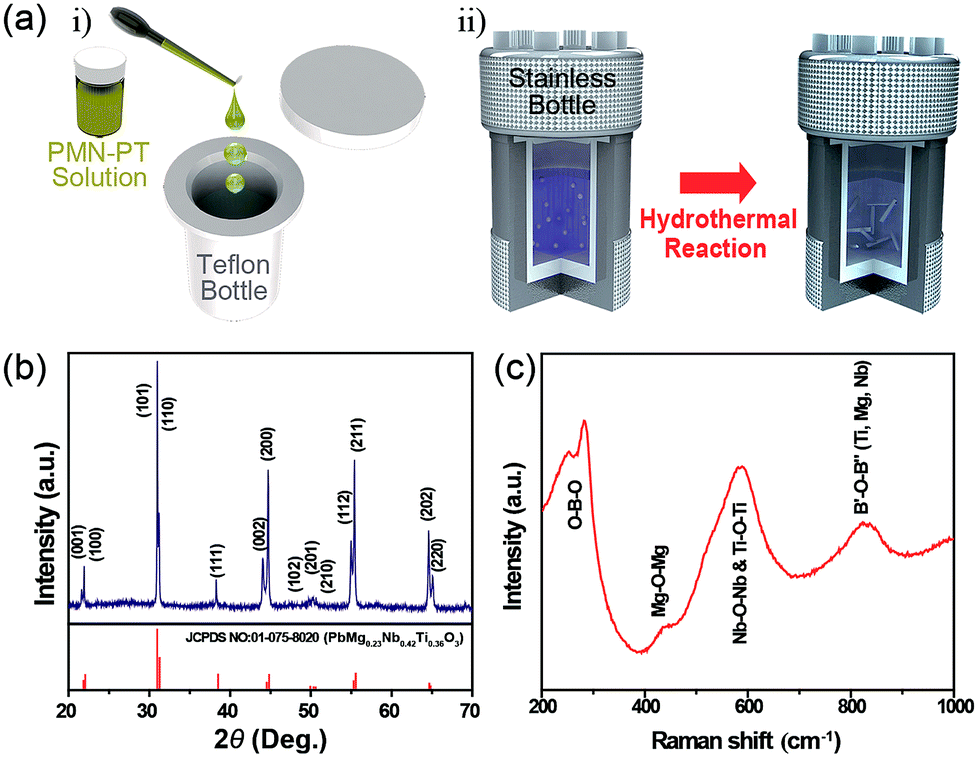 | ||
| Fig. 1 (a) Schematic representation of the synthesis procedure for the preparation PMN–PT NWs by a hydrothermal method. (i) PMN–PT solution prepared by a sol–gel method used as seed. (ii) PMN–PT nuclei grown as NWs under hydrothermal conditions. (b) XRD pattern of PMN–PT NWs. (c) Raman spectrum of PMN–PT NWs. | ||
SEM image in Fig. 2a shows that the synthesized PMN–PT powders contains a large quantity of randomly oriented nanowires with diameter of about ∼100 nm and length of about nm and 10 μm, respectively. The lattice fringes were clearly observed in HR-TEM image (the left-top inset of Fig. 2b), confirming the crystalline nature. In addition, selected area diffraction (SAED) pattern obtained the PMN–PT NW shown in Fig. 2b (right-bottom image) depicts clearly the single crystalline nature of the nanowire. Further, the spacing between the lattice fringes was calculated to be 2.82 Å, which corresponded to the (110) plane of the tetragonal PMN–PT phase. The XRD and HRTEM results confirms the orientation of NWs growth is parallel to the (110) direction of tetragonal PMN–PT crystal. Fig. 2e displays the typical scanning transmission electron microscopy (STEM) image of a single NW. Energy dispersive X-ray spectroscopy (EDS) mapping of PMN–PT NW utilizing scanning transmission electron microscopy (STEM) in Fig. 2c confirms the presence all the elements (Pb, Nb, Mg, Ti, and O) and all elements were distributed uniformly along the NWs.
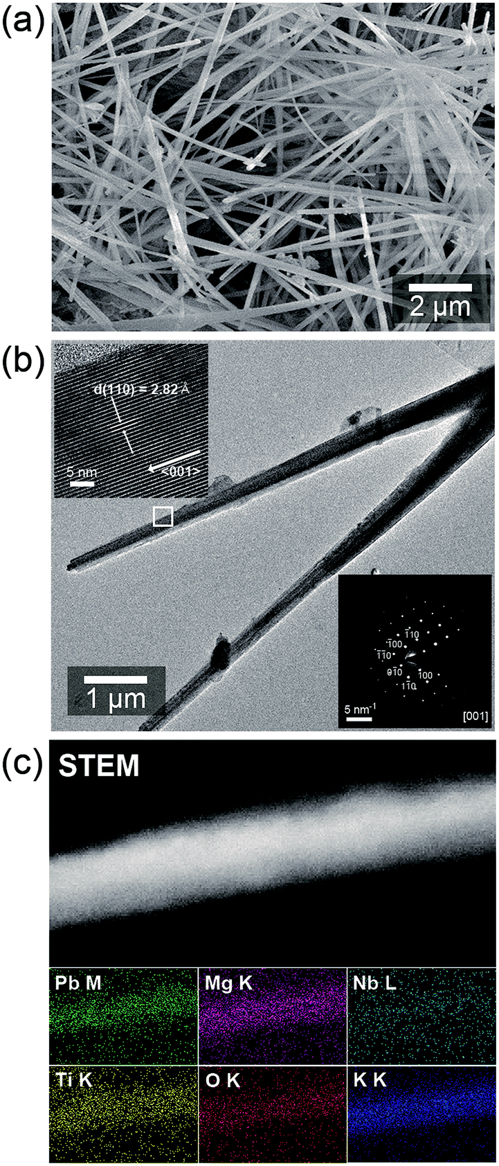 | ||
| Fig. 2 (a) SEM image of PMN–PT NWs synthesized by a hydrothermal method. (b) TEM image of PMN–PT NWs. The Left-top inset is a HRTEM image of a single NW showing that lattice fringes of the (110) plane and the right-bottom image shows the SAED pattern when the electron beam is coherent along the [001] plane. (c) STEM image and EDS mapping of a PMN–PT NW. | ||
The formation of PMN–PT NWs under hydrothermal condition follows a “Dissolution–Recrystallization” mechanism. In this procedure, the precursor materials for Pb–Mg and Nb–Ti elements were first dissolved separately in the PEG and MeOH mixture with THOME. It should be noted that THOME was selected as a complexing agent due to its high metal complexation ability.31 The above solutions can result in a homogenous mixture, and they contained all the cationic species. Then, the organic volatiles were removed from the precursor solutions to form the viscous stock solutions. Initially, a white colored amorphous hydroxide precursor [Pb(OH)2, Mg0.216Nb0.433Ti0.35O(OH)2] was formed when 5 mL of a PMN–PT stock solution was added into the 60 mL of a KOH solution.24
It is believed that the solubility of the amorphous precursor solution can increase under hydrothermal condition at 200 °C and the strong alkaline medium. Therefore, the amorphous hydroxide particles are able to be dissolved as soluble ions [HPbO2−] and [Mg0.216Nb0.433Ti0.35(OH)x4−x (4 < x < 6)]. Once the super-saturation level is reached in the hydrothermal solution, the primary PMN–PT nuclei can be grown by the reprecipitation of dissolved precursor ions. Thereby, the overall reaction mechanism involves with the formation of metal hydroxide complex during the initial step and followed by formation metal oxide nanowires through “Dissolution–Recrystallization” mechanism.
The selective adsorption of PEG-200 on the surface PMN–PT crystals was considered to play an important role as a capping agent for the formation of NWs. The polymer was adsorbed on the (110) plane with the highest surface energy, which can repress the radial growth direction and induce the longitudinal growth along the c-axis of the PMN–PT nuclei. This mechanism was revealed in the previous reports about the combination of polymeric capping agents for some tetragonal 1-D PZT structures.32
In order to evaluate the ability of a single PMN–PT NW in power generation, we fabricated a simple PEH device to scavenge an output signal from a single PMN–PT NW. The scheme in Fig. 3a illustrates our PEH device fabrication design for measuring the output performance from a single PMN–PT NW and the further detailed procedure given in the Experimental section. A photograph of the flexible PEH device based on a single PMN–PT NW connected with copper wires for measuring the output signals, were displayed in Fig. 3b. The edges of a single PMN–PT NW were connected to Au electrodes by FIB-Pt deposition process (see Fig. 3c).
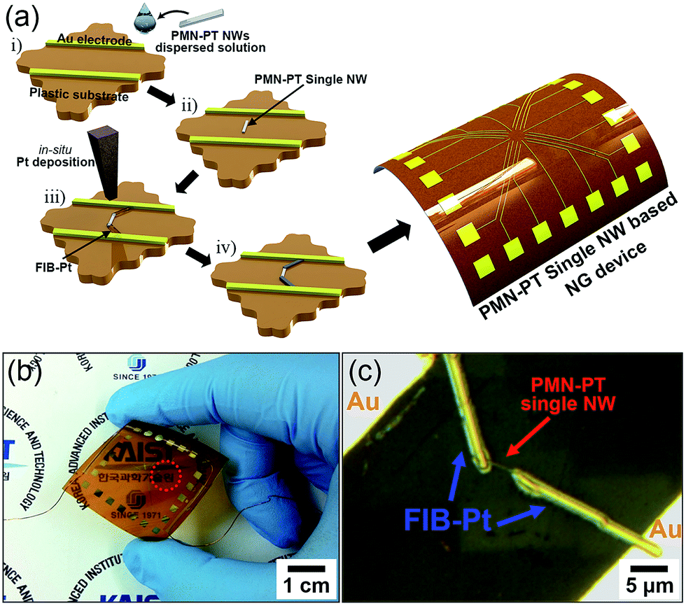 | ||
| Fig. 3 (a) Schematic illustration of the overall fabrication process for a single PMN–PT NW based PEH. (b) Photograph of a flexible nanoscale PEH device connected with Cu wires. (c) PMN–PT NW connected with Au electrodes by the FIB-Pt process. | ||
The working mechanism of the PEH based on a single PMN–PT NW is explored and the short-circuit current and open-circuit voltage were measured by a customized measurement system. Fig. 4a shows a magnified SEM image of nanoscale PEH device in which a single PMN–PT NW (∼5 μm long) is connected with Au electrodes by a Pt docking line using the FIB technique. The output signals were generated when the nanoscale PEH device based on single PMN–PT NW is repeatedly bent along the axial direction by a bending machine. Under repeatedly bending and unbending motions as shown in the scheme of Fig. 4b, the corresponding output voltage and current signal generations are shown in Fig. 4c and d. By the bending motions with a strain of 0.283% (corresponding to a bending radius of 2.20 cm and applied force of 1.1 μN with elastic modulus of 20 GPa (ref. 33)) at a straining rate of 2.32% s−1, the PMN–PT single NW-based PEH device, which had a length of about 5 μm and a diameter of 140 nm, repeatedly generated an output voltage of 9 mV [corresponding to a piezoelectric voltage coefficient (g33) of 40 × 10−3 V m N−1] and a current pulse of 1.5 nA. The current density (9.7 A cm2) and power density (175.4 W cm−3) calculated from single PMN–PT NW based PEH is higher than previously reported lateral single NW-based PEH devices.18,21,22 Subsequently, we performed the switching polarity test to verify that the output signal was generated originally from the piezoelectric effect of PMN–PT NW. In a forward connection, the positive and negative signals were measured with respect to the bending and unbending motions, as presented in Fig. 4c. In the case of a reverse connection, the NG device based a single PMN–PT NW was reversely connected to the measurement system, and the obtained average output signal were similar to that of the forward connection, but the polarity was inversed (Fig. 4d), which confirmed that the signals came from the piezoelectric effect of the PMN–PT NW.
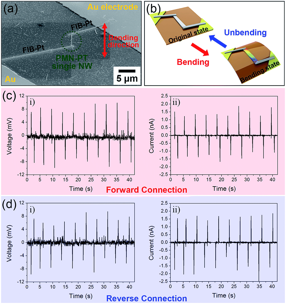 | ||
| Fig. 4 (a) SEM image of a PEH device based on a single PMN–PT NW docked to Au electrodes by the FIB-Pt process. (b) Scheme of the original and bending states of the nanoscale PEH based on a single PMN–PT NW. Open-circuit voltage and short-circuit current generation of a single PMN–PT NW based PEH device during bending/unbending conditions with (c) forward and (d) reverse connection to a measuring equipment. | ||
For the purpose of demonstrating practical energy harvesting applications using the piezoelectric effect of PMN–PT NWs, we adopted a familiar NCG fabrication technique with simple, low-cost, and scalable spin-casting (see Fig. S1 of ESI†).28 As shown in the schematic representation of Fig. S1a,† the PMN–PT NWs were embedded in the PDMS matrix without any dispersing agents to produce the polymer-based piezoelectric composites. Next, a selected piezoelectric thick layer were sandwiched between two ITO-coated PET substrates that acted as a current collector. To measure the output signals, both electrodes were connected with Cu wires by conductive epoxy. The further details of the fabrication process is described in the Experimental section. Fig. S1b† shows a photograph of the actual fabricated NCG device with an effective area of 3 × 3 cm2, which could be bent by human fingers. The output signals were generated from the PMN–PT nanocomposite by mechanically stressing the device using a linear motor, which were recorded in real time by a measurement unit and a computer. The corresponding output voltage and current generation graph is shown in Fig. S1c.† The NCG made of PMN–PT NWs harvested a maximum open-circuit voltage of 4.0 V and short-circuit current of 400 nA; these values were created by the mechanical bending deformations with the displacement of 5 mm at the deformation rate of 0.2 m s−1. By the well-known switching polarity test results (Fig. S1d†), we confirmed that the measured output signals were induced from the piezoelectric effect of the NCG device.
Conclusions
In summary, we have used a simple hydrothermal method to synthesize single-crystalline 0.65Pb(Mg1/3Nb2/3)O3–0.35PbTiO3 NWs with an average length of 10 μm and a diameter of 140 nm. We have demonstrated a single PMN–PT NW based PEH by simple transferring the NW onto a flexible plastic substrate. The output performance of the single PMN–PT NW reached the maximum output voltage of 9 mV and a maximum current of 1.5 nA with a power density of 175.4 W cm−3, which are higher than those of previously reported lateral aligned single NW-based PEH devices. Furthermore, the NCG device was made by dispersing the hydrothermally synthesized PMN–PT NWs into a PDMS matrix without using any dispersants. The open-circuit voltage and short-circuit current generated from the PMN–PT NWs-based composite generator reached up to ∼4 V and ∼400 nA, respectively, under periodically bending and unbending conditions. Our findings suggest the practical characterization of flexible PEH based on a single PMN–PT NW and the feasibility of an NCG device made of PMN–PT NWs and a PDMS elastomer, which may bring interesting applications in the field of flexible self-powered energy systems.Acknowledgements
This work was supported by the National Research Foundation (NRF) of Korea grant funded by the Korea government (MSIP) (No. 2016R1C1B1006456).Notes and references
- S. Priya and D. J. Imman, Energy Harvesting Technologies, 2009 Search PubMed.
- Z. L. Wang, Nanogenerators for Self-powered Devices and Systems, 2011 Search PubMed.
- Y. Qi and M. C. McAlpine, Energy Environ. Sci., 2010, 3, 1275–1285 CAS.
- C. R. Bowen, H. A. Kim, P. M. Weaver and S. Dumn, Energy Environ. Sci., 2014, 7, 25–44 CAS.
- C. Sun, J. Shi and X. Wang, J. Appl. Phys., 2010, 108, 034309–034311 CrossRef.
- S. Xu, Y. Qin, C. Xu, Y. Wei, R. Yang and Z. L. Wang, Nat. Nanotechnol., 2010, 5, 366–373 CrossRef CAS PubMed.
- J. Yan and Y. G. Jeong, ACS Appl. Mater. Interfaces, 2016, 8, 15700–15709 CAS.
- X. Chen, S. Xu, N. Yao and Y. Shi, Nano Lett., 2010, 10, 2133–2137 CrossRef CAS PubMed.
- Z. L. Wang and J. Song, Science, 2006, 312, 242–246 CrossRef CAS PubMed.
- X. D. Wang, J. H. Song, J. Liu and Z. L. Wang, Science, 2007, 316, 102–105 CrossRef CAS PubMed.
- Z. L. Wang, Adv. Funct. Mater., 2008, 18, 3553–3567 CrossRef CAS.
- C. T. Huang, J. H. Song, W. F. Lee, Y. Ding, Z. Y. Gao, Y. Hao, L. J. Chen and Z. L. Wang, J. Amer. Ceram. Soc., 2010, 132, 4766–4771 CAS.
- Y. Qi, J. Kim, T. D. Nguyen, B. Lisko, P. K. Purohit and M. C. McAlpine, Nano Lett., 2011, 11, 1331–1336 CrossRef CAS PubMed.
- C. Y. Chen, T. H. Liu, Y. Zhou, Y. Zhang, Y. L. Chueh, Y. H. Chu, J. H. He and Z. L. Wang, Nano Energy, 2012, 1, 424–428 CrossRef CAS.
- A. Koka, Z. Zhou and H. A. Sodano, Energy Environ. Sci., 2014, 7, 288–296 CAS.
- Y. F. Lin, J. Song, Y. Ding, S. Yuan and Z. L. Wang, Appl. Phys. Lett., 2008, 92, 022105 CrossRef.
- T. Huang, J. Song, W. F. Lee, Y. Dong, Z. Gao, Y. Hao, L. J. Chen and Z. L. Wang, J. Am. Chem. Soc., 2010, 132, 4766–4771 CrossRef PubMed.
- R. S. Yang, Y. Qin, L. M. Dai and Z. L. Wang, Nat. Nanotechnol., 2009, 4, 34–39 CrossRef CAS PubMed.
- R. S. Yang, Y. Qin, C. Li, G. Zhu and Z. L. Wang, Nano Lett., 2009, 9, 1201–1205 CrossRef CAS PubMed.
- G. Zhu, R. Yang, S. Wang and Z. L. Wang, Nano Lett., 2010, 10, 3151–3155 CrossRef CAS PubMed.
- J. M. Wu, C. Xu, Y. Zhang and Z. L. Wang, ACS Nano, 2012, 6, 4335–4340 CrossRef CAS PubMed.
- T.-C. Hou, Y. Yang, Z.-H. Lin, Y. Ding, C. Park, K. C. Pradel, L.-J. Chen and Z. L. Wang, Nano Energy, 2013, 2, 387–393 CrossRef CAS.
- H. Fu and R. Cohen, Nature, 2000, 403, 281–283 CrossRef CAS PubMed.
- S. Xu, G. Poirier and N. Yao, Nano Lett., 2012, 12, 2238–2242 CrossRef CAS PubMed.
- S. Xu, Y. W. Yeh, G. Poirier, M. C. McAlpine, R. A. Register and N. Yao, Nano Lett., 2013, 13, 2393–2398 CrossRef CAS PubMed.
- F. Wu, W. Cai, Y. W. Yeh, S. Xu and N. Yao, Sci. Rep., 2016, 6, 22513 CrossRef CAS PubMed.
- K. Babooram and Z.-G. Ye, Chem. Mater., 2004, 16, 5365–5371 CrossRef CAS.
- K.-I. Park, S. B. Bae, S. H. Yang, H. I. Lee, K. Lee and S. J. Lee, Nanoscale, 2014, 6, 8962–8968 RSC.
- E. Ching-Prado, J. Vac. Sci. Technol., A, 1996, 14, 762 CAS.
- M. Shen, G. G. Siu, Z. K. Xu and W. Cao, Appl. Phys. Lett., 2005, 86, 252903 CrossRef.
- N. Sriprang, D. Kaewchinda, J. D. Kennedy and S. J. Milne, J. Amer. Ceram. Soc., 2000, 83, 1914–1920 CrossRef CAS.
- G. Xu, Z. Ren, P. Du, W. Weng, G. Shen and G. Han, Adv. Mater., 2005, 17, 907–910 CrossRef CAS.
- D. Viehland and J. F. Li, J. Appl. Phys., 2003, 94, 7719–7722 CrossRef CAS.
Footnotes |
| † Electronic supplementary information (ESI) available. See DOI: 10.1039/c6ra24688e |
| ‡ Equal contributors. |
| This journal is © The Royal Society of Chemistry 2017 |