
Enhancing light trapping of macroporous silicon by alkaline etching: application for the fabrication of black Si nanospike arrays†
G.
Loget
 *a,
A.
Vacher
a,
B.
Fabre
a,
F.
Gouttefangeas
b,
L.
Joanny
b and
V.
Dorcet
c
*a,
A.
Vacher
a,
B.
Fabre
a,
F.
Gouttefangeas
b,
L.
Joanny
b and
V.
Dorcet
c
aInstitut des Sciences Chimiques de Rennes, UMR 6226 CNRS, Matière Condensée et Systèmes Electroactifs (MaCSE), Université de Rennes 1, Campus de Beaulieu, 35042 Rennes Cedex, France. E-mail: gabriel.loget@univ-rennes1.fr
bScanMAT-Cmeba, UMS 2001 CNRS, Université de Rennes 1, Campus de Beaulieu, 35042 Rennes Cedex, France
cInstitut des Sciences Chimiques de Rennes, UMR 6226 CNRS, Pôle Ressources Administratives Techniques et Scientifiques (PRATS), Université de Rennes 1, Campus de Beaulieu, 35042 Rennes Cedex, France
First published on 27th May 2017
Abstract
The synthesis of highly absorbing silicon (black Si (BSi)) is a very active research topic with promising applications in the field of sustainable energies, ultrasensitive sensing and antibacterial materials. Here, we show that extended alkaline etching of macroporous Si, fabricated by photoelectrochemical etching, drastically influences the surface structures as well as their optical properties. We demonstrate that this treatment can considerably improve the light trapping of the surface and we finally show that it is possible to use it for fabricating very quickly highly-absorbing arrays of sharp and crystalline BSi nanospikes (NSpikes).
Introduction
The high reflection of light by silicon surfaces is a critical issue for many Si-based devices as it limits electron–hole pair generation and therefore restrains the performances of Si-based energy conversion devices such as solar cells (SCs), water-splitting photoelectrochemical cells (PECs) and photodetectors.1–5 It is known that enhanced light absorption can arise from nano- and microstructured Si surfaces that induce respectively a smooth transition of refractive index or multiple internal reflections.1,4,6,7 In this context, top down micro- and nanostructuration of mono- or polycrystalline Si surfaces is highly appealing for boosting photon absorption and enlarging surface areas while conserving the properties of bulk Si. The fabrication of structured and highly absorbing Si, referred to as Black Si (BSi), is, therefore, a very active research topic in materials with applications for renewable energy and photonics1–4,8–10 and also, as recently demonstrated, for designing efficient surface-enhanced Raman scattering (SERS)11 surfaces or biomimetic antibacterial materials.12 Several techniques can be used to enhance light absorption. Dry etching processes such as reactive ion etching (RIE) or deep RIE are usually employed to fabricate grass-like nanotip arrays with broadband low reflectance.13–15 In addition, the group of Mazur reported that irradiation of Si wafers with femtosecond-laser pulses in the presence of a halogen or a fluoride-containing gas can be used to create random arrays of absorbing nanocones.16 If these dry techniques are highly tunable, their main drawbacks are their cost and the handling of gases. Conversely, wet chemical approaches usually require simple experimental setups and hold fast etching rates which make them highly promising for the large-scale production of BSi.2 Among them, alkaline etching (AE) of Si by KOH17 or tetramethylammonium hydroxide solutions,18,19 is largely used for structuring solar cells and for manufacturing microelectromechanical systems. While these processes can be used to create random arrays of Si micropyramids, the resulting weighted reflectivity is usually limited.20,21 Stain etching can also be used to produce an antireflective porous layer,22,23 however, the reproducibility of this process is often discussed.2,24 Metal-assisted chemical etching is a very popular method for manufacturing absorbing Si nanowires (SiNWs)25 and porous BSi that can improve the performances of SCs,8 however this process can contaminate the surface with metals.2 Besides, electrochemical methods are generally low-cost and allow a high degree of tunability. For instance, it has been reported that the electroreduction of silica26 can lead to BSi.27 Electrochemical etching (EE)28,29 and photoelectrochemical etching (PEE)30–33 of Si are cost-effective and easy to implement methods that are intensely used to grow micropores (pores width < 2 nm), mesopores (2 nm < pores width < 50 nm) as well as random or organized arrays of macropores (pores width > 50 nm) on mono- and polycrystalline Si.24,34–36 In particular, great developments have been made on PEE of n-type Si illuminated from the backside by Lehman and Föll who developed the “space charge region pore formation model” and used it to fabricate well controlled Si macropore arrays.30,34 Levy-Clement et al. have reported the formation of macropores on frontside illuminated n-type Si,33,37 however much less work has been devoted to this structuration process.34 EE and PEE can be used to produce BSi, notably, it has been reported that thin layers of micro- and mesoporous Si can lead to a substantial reflectivity decrease.38 In addition, thicker macropore layers can also confer antireflective properties to Si.39–42 Interestingly, our group and others have recently shown that BSi made of organized or random macropores fabricated using PEE exhibits enhanced performance as a photoanode for water splitting PECs.40,41 During typical syntheses of macroporous Si, a short exposure of PEE-etched porous Si, in weakly concentrated KOH at ambient temperature is commonly employed to smoothen the pore walls.30,33,36 However, the effect of this treatment on porous Si seems to have been overlooked and, to the best of our knowledge, the extended etching of porous Si by highly concentrated and hot alkaline solutions has never been studied so far. In this work, we show that this treatment drastically influences the surface structures as well as their optical properties. We demonstrate that it can considerably improve the light trapping of the surfaces and we finally use this effect to produce very quickly (∼5 min) BSi made of Si NSpikes on relatively large areas.Experimental section
Materials and reagents
Acetone (MOS electronic grade, Erbatron from Carlo Erba) and anhydrous ethanol (RSE electronic grade, Erbatron from Carlo Erba) were used without further purification for cleaning the silicon surfaces. The ultrapure water had a resistivity of 18.2 MΩ cm (Purelab Classic UV from Veolia Water STI). HF (50% aq. solutions), and KOH (>85%, Reag. Ph. Eur.) were purchased from Sigma-Aldrich. The n-type silicon wafers (1–5 Ω cm resistivity, phosphorus doped, double side polished, 250–275 μm thickness, (100)) were purchased from Siltronix. The chemicals used for the cleaning and etching of the Teflon vials (30% H2O2 and 96–97% H2SO4) were of VLSI (H2O2, from Sigma-Aldrich) and MOS (H2SO4 from BASF) semiconductor grade. The absolute ethanol used for PEE and isopropanol were purchased from VWR.Photoelectrochemical etching
All Teflon vials and tweezers used for cleaning of silicon were previously decontaminated in 3/1 v/v concentrated H2SO4/30% H2O2 at 100 °C for 30 min, followed by copious rinsing with ultrapure water. Caution: the concentrated aqueous H2SO4/H2O2 (piranha) solution is very dangerous, particularly in contact with organic materials, and should be handled extremely carefully. The n-type silicon (100) wafers were cut in 1.5 × 1.5 cm2 squares and degreased by sonication (10 min) in acetone, ethanol and ultrapure water in Teflon vials. They were then dried under an Ar stream. One side of the Si surface was scratched using a diamond glass cutter and sandpaper to create trenches in the native oxide layer. For the photoelectrochemical etching, the surfaces were inserted into a home-made open-top O-ring cell (the diameter of the O-ring was 1 cm). The electrical contact was achieved by pressing aluminum foil between the scratched Si surface and a copper plate. The counter electrode was a Pt ring (1 cm diameter) placed above the silicon surface. The cell was filled with 4 mL of the electrolyte solution containing absolute ethanol and 50% aq. HF at a 1/1 v/v ratio. The Si surface was irradiated from the electrolyte side with a solar simulator (LS0106, LOT Quantum Design) equipped with an AM 1.5 G filter and a current of 100 mA was applied for 4 min with a LAB-SMP (ET System) power supply. During the PEE, the current flowing through the cell was monitored using a Keithley 2000 and recorded on a computer via a homemade Labview program. The surface was then copiously rinsed with absolute ethanol and dried under an argon flow.Alkaline etching
The AE solution was freshly prepared by dissolving KOH (500 g L−1, 8.9 M) in a water/isopropanol (2% vol.) mixture. This solution was maintained at 80 °C and vigorously stirred (350 rpm) in a Pyrex beaker. After PEE, the ethanol-rinsed and dried porous Si surfaces were directly exposed to the AE solution for the desired amount of time (between 2 s and 2 min). After that, they were dipped in ultrapure water to stop the etching, rinsed copiously and dried with Ar.Surface characterization
Scanning electron microscopy (SEM) was performed using a JSM 7100F (JEOL). SEM image analysis was performed using the ImageJ software. Energy-dispersive X-ray spectroscopy was carried out using a Silicon Drift Detector (SDD) – X-Max (80 mm2) and the AZtecEnergy software (Oxford Instruments). Transmission electron microscopy (TEM) was performed using a JEOL 2100 LaB6 microscope operating at 200 kV equipped with a GATAN Orius 200D CCD camera for diffraction and Bright Field (BF) image acquisition and with a GATAN Ultra-Scan 1000 CCD camera for high-resolution image acquisition. The reflectance spectra were acquired on a Shimadzu UV-3600Plus spectrophotometer with an integrating sphere (ISR-603). A sample of extra pure BaSO4 was used as the 100% reflectance reference (Nacalai Tesque). A Teflon mask was used to perform the measurement and ensure a good reproducibility. The total reflectance was measured with an incident beam with an angle of 8° to include the specular component.Results and discussion
PEE was performed with a two-electrode setup, in the photoelectrochemical cell depicted in the inset of Fig. 1b with a classical ethanol-based electrolyte containing HF.24 We employed light irradiation to supply holes for oxidizing the n-type Si surface, which was illuminated from the top of the cell (from the electrolyte side). It is worth mentioning that this illumination configuration, as well as the spectral distribution of the incident light (AM 1.5 G), have an importance on the pore morphology. The PEE parameters were kept constant for all the samples made in this work: a current density j = 0.13 A cm−2 was applied for 4 min in every case. As shown in Fig. S1 (ESI†), the potential typically stabilized at ∼20 V after 40 s. Under these conditions, the combined action of photogenerated holes and fluorides in solution led to the dissolution of the Si surface and the formation of a porous Si (PSi) layer, as described by the following reaction:24,30| Si(s) + 6HF(aq) + 2h+ → SiF62−(aq) + H2(g) + 4 H+(aq) | (1) |
| Si(s) + 2OH−(aq) + 2H2O(aq) → SiO2(OH)22−(aq) + 2H2(g) | (2) |
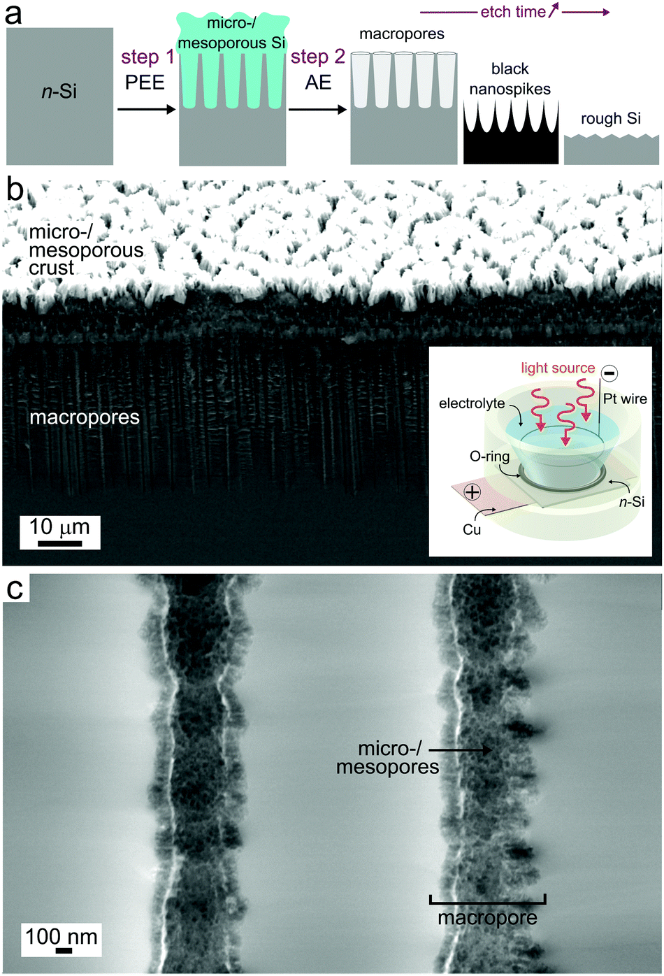 | ||
| Fig. 1 (a) Two-step structuration procedure involving first photoelectrochemical etching (PEE) followed by alkaline etching (AE). (b) Low magnification tilted view (45°) showing the macropores covered by a micro-/mesoporous transitional layer (Si layer obtained after a PEE of 4 min at 0.13 A cm−2). Inset: Scheme of the photoelectrochemical setup used for PEE. (c) High magnification cross-section showing the inner walls of two macropores. | ||
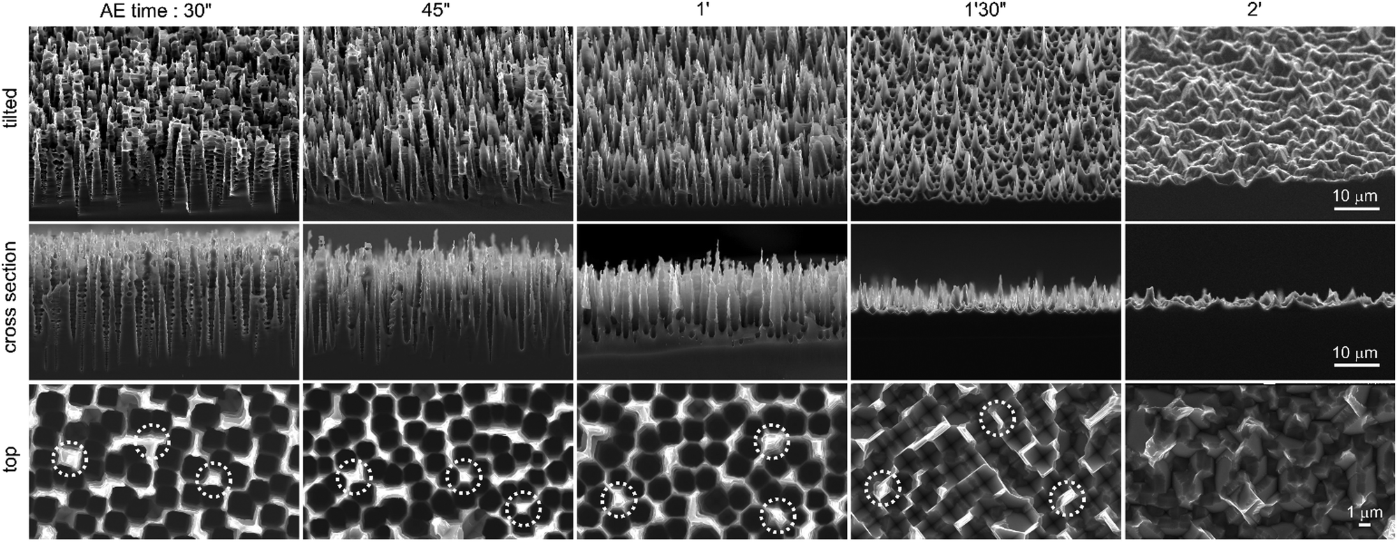 | ||
| Fig. 2 SEM images showing the Si porous layer obtained after different times of AE (note that in all cases, the surface was patterned with an identical PEE step of 4 min at 0.13 A cm−2). The time of AE is indicated on the top of each column. Top, middle and bottom rows show tilted (45°), cross-section and top views, respectively (for the sake of visibility, three areas where an NSpike forms are indicated by white dotted circles in the four first images of the bottom row). | ||
Due to the enormous surface area of micro-/mesoporous Si (typically in the order of 100 to 1000 m2 cm−3),44 this material reacted at a much higher rate with the alkaline solution than the bulk Si. Consequently, the PSi crust that was observed on the top of the surface after PEE (Fig. 1b) dissolved quasi-instantaneously. Fig. S3 (ESI†) shows that this top layer disappeared after 2 s of reaction. However, a close investigation of the macropore walls for surfaces that were exposed for 2 s and 15 s (Fig. S3d and S4d, ESI†) revealed that a micro-/mesoporous layer was still present inside the macropores. We attribute this to the lack of hydroxide inside the pores during the first seconds of AE, caused by the limited accessibility within these deep structures. After 30 s of reaction, only bulk, macroporous Si could be observed, suggesting that all micro-/mesoporous Si was etched.
Although SEM reveals that the micro-/mesoporous Si was totally dissolved after 30 s, the surface continuously reacted with the hydroxides and the macropore morphology consequently evolved during the exposure to the KOH solution, as shown in Fig. 2. The tilted and cross-section SEM views clearly show the evolution of the micro- and nanostructures as reaction (2) occurs (Fig. S6 (ESI†), which presents the layer thickness as a function of etching time, reveals an etching rate of 320 nm s−1). Fig. 2 shows that at 30 s of AE, the structures could be considered conical macropores. As it can be seen in the SEM top views (in the bottom row of Fig. 2), the thickness of the pore walls was not homogeneous, therefore some sections of the walls dissolved at a slower rate than others. This is particularly true for the walls that were shared by several macropores (typically >3–4), some of which are indicated by the white circles in the SEM top views (bottom row of Fig. 2).
As the macropores opened, it can be observed that Si NSpikes started to develop in these specific areas, which were initially thicker than the rest of the wall. This was caused by a faster etching of the top of the pore walls than the bottom, which we attribute to the gradual decrease of the hydroxide concentration along the pores, caused by their low diffusion within the cavities. The formation of these NSpikes can be observed in the cross-section images obtained from 45 s and they are particularly pronounced for the samples immersed in the AE solution for 1 and 1.5 min. At 1.5 min, the pores totally disappeared due to the full dissolution of their walls and the surface was only composed of 5 μm long NSpikes, spaced by inverted pyramid pits (with exposed (111) faces), resulting from the anisotropic AE of the macropore bottoms.17–19 Ultimately, when the reaction was carried out for extended times (here 2 min, as shown in the last column of Fig. 2), the NSpikes were totally etched and only a rough Si surface remained. We observed an intriguing color change in the surface occurring during the AE reaction, and have consequently investigated the optical properties of the structured surfaces. In order to simply visualize the color changes as a function of the AE time, several samples were prepared with different AE times, and their photographs are displayed in Fig. S7 (ESI†). The total reflectance as a function of the reaction time was also measured and the corresponding spectra are shown in Fig. 3. The reflectance of planar (100) Si was between 50% and 30%, with an average total reflectance of 37% in the visible range (400–800 nm), which is in good agreement with previous reports.2 After PEE, the surface became mainly bright yellow. We attribute this color to the high scattering of light by the micro-/mesoporous Si crust present on the top of the macropores (Fig. S2, ESI†). We can state from Fig. 3 that the AE was divided into two periods of time.
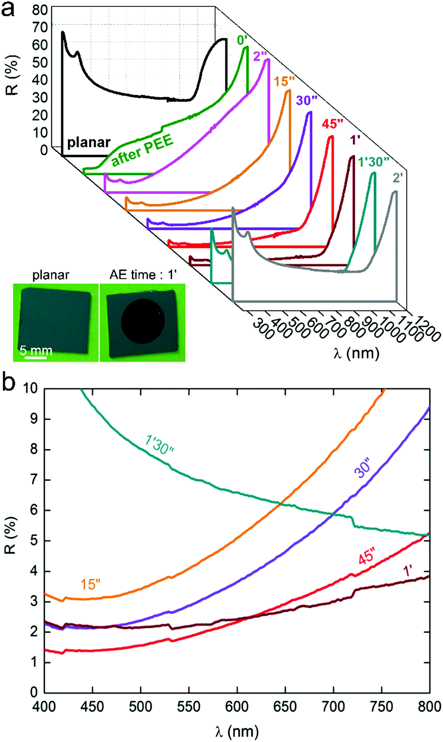 | ||
| Fig. 3 (a) Series of UV-vis-NIR total reflectance spectra showing the evolution of the reflectance as a function of the AE time. Inset: Photograph of a planar Si surface (left) and a Si NSpike surface (right). (b) Reflectance in the visible range for the most absorbing samples. | ||
During the first stage, i.e. for AE times between 2 s and 1 min, the surface reflectance continuously decreased, showing that the light trapping was considerably enhanced by the opening of the macropores and the growth of the Si NSpikes (Fig. 2) that allowed for a better light penetration in these high-aspect-ratio structures and favored multiple internal reflections. As shown in Fig. 3b, the optimal “blackness”, i.e. the lower reflectance, was obtained for AE times of 45 s and 1 min, corresponding to the surfaces bearing the sharp and high aspect ratio Si NSpike arrays. During the second stage of AE (after 1 min), the surface reflectance increased, due to the lowering of the aspect ratio of the nanostructures, as shown in Fig. 2. The average total reflectance for the best light trapping surfaces was ∼3% in the visible range, meaning that this treatment induced a reflectance decrease of 90% with respect to the polished planar Si. Additional optical measurements, performed with another spectrophotometer were in very good agreement (Fig. S8, ESI†). This reflectance is much lower than that of our previously reported macroporous Si41 and the typical values obtained for the widely used micropyramid arrays.18–21 This value is rather in the same range as those reported for Si surfaces structured by femtosecond laser pulses,16 modified with a porosity gradient38 or with regular arrays of Si modulated macropores,39,40 and our process is simpler. These results show that: (i) AE can have a drastic effect on the shape of macroporous Si and can result in totally new nanostructures and (ii) the so-fabricated structures can highly enhance the light absorption.
We now pay special attention to the Si NSpike arrays that presented the best light trapping because they are very promising for energy conversion, SERS or biomimetic antibacterial devices.10–12 More samples were prepared using the protocol described above (with an AE time of 1 min) and were further characterized, as shown in Fig. 4. In the low magnification view (Fig. 4a), it can be seen that the NSpikes covered the whole surface of the Si wafer in a grass-like fashion (see also Fig. S9, ESI†); based on analyses of SEM top views, the surface density was estimated to be 7 × 104 mm−2. Interestingly, the shape of the so-fabricated NSpikes was closely similar to that of structures obtained by RIE,15 although their length was, in our case, at least one order of magnitude greater. High magnification SEM images, shown in Fig. 4b and c reveal that the tips of the spikes were sharp and highly faceted. The Si NSpikes were further investigated by transmission electron microscopy (TEM), which allowed the observation of individual Si NSpikes (Fig. 4d) detached from the Si surface by scratching. TEM images, shown in Fig. 4d and Fig. S10 (ESI†), as well as the diffraction pattern in the inset of Fig. 4d, reveal that the Si NSpikes were monocrystalline and confirmed their orientation in the [100] direction. Interestingly, the high-resolution (HR) TEM observations presented in Fig. 4e and Fig. S10 (ESI†) confirm that the NSpike apexes were in the range of 10 nm and showed that the Si NSpikes were covered by a ∼3 nm-thick native amorphous SiO2 layer. EDS analyses of the NSpike arrays, presented in Fig. 4f for a large area (see Fig. S11 (ESI†) for the analysis area), and in Fig. S12 (ESI†) for an individual Si NSpike both show that Si was the only detected element, which demonstrates that the surfaces were free of potassium or fluorine contaminants that may have an undesired influence on the Si properties.
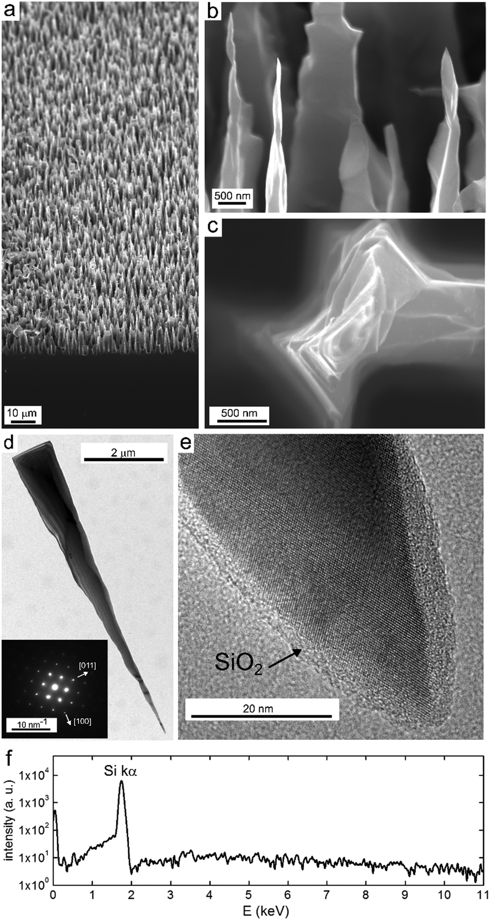 | ||
| Fig. 4 (a–c) SEM images showing: (a) a low magnification tilted view (45°), (b) a high magnification tilted view and (c) a high magnification top view of an NSpike surface that was obtained with an AE time of 1 min. (d) Bright-field TEM image of an individual Si NSpike detached from a Si surface that underwent AE for 1 min. Inset: Diffraction pattern obtained in the middle of the Si NSpike. (e) High-resolution TEM image showing the tip of the corresponding Si NSpike. (f) EDS spectrum of the corresponding surface (note that the y-axis is in logarithmic scale). | ||
Conclusions
In summary, we have reported the effect of extended AE on macroporous silicon. We have shown that this surface treatment can lead to new nanostructures that have a significant effect on the light trapping of the surface.We have shown by SEM, TEM, and optical measurements that reaction optimization allows the generation of arrays of sharp, crystalline and highly absorbing Si NSpikes presenting an average reflectance of 3% in the visible range. Due to the potential scalability and the simplicity of the method, it is highly promising because such arrays could have straightforward applications for various Si-based devices, in particular for improving the performances of SCs,5 as well as in artificial photosynthesis for producing highly efficient Si-based PEC photoelectrodes.1 Last but not least, such spikes would be appealing for ultrasensitive biodetection devices based on surface-enhanced Raman scattering (SERS)11 or for designing antibacterial materials.12
Acknowledgements
This work is funded by ANR (project EASi-NANO, ANR-16-CE09-0001-01). Thierry Guizouarn is acknowledged for making the labview program used for electrochemical etching. Dr F. Cheviré is acknowledged for discussion about the spectrophotometer and reflectance measurements. The authors acknowledge the THEMIS platform for TEM facilities.References
- K. Sun, S. Shen, Y. Liang, P. E. Burrows, S. S. Mao and D. Wang, Chem. Rev., 2014, 114, 8662–8719 CrossRef CAS PubMed.
- X. Liu, P. R. Coxon, M. Peters, B. Hoex, M. Cole and D. J. Fray, Energy Environ. Sci., 2014, 7, 3223–3263 CAS.
- J. E. Carey, C. H. Crouch, M. Shen and E. Mazur, Opt. Lett., 2005, 30, 1773–1775 CrossRef PubMed.
- F. Priolo, T. Gregorkiewicz, M. Galli and T. F. Krauss, Nat. Nanotechnol., 2014, 9, 19–32 CrossRef CAS PubMed.
- J. Zhu, Z. Yu, S. Fan and Y. Cui, Mater. Sci. Eng., R, 2010, 70, 330–340 CrossRef.
- S. Lou, X. Guo, T. Fan and D. Zhang, Energy Environ. Sci., 2012, 5, 9195–9216 CAS.
- M. Toma, G. Loget and R. M. Corn, Nano Lett., 2013, 13, 6164–6169 CrossRef CAS PubMed.
- J. Oh, H.-C. Yuan and H. M. Branz, Nat. Nanotechnol., 2012, 7, 743–748 CrossRef CAS PubMed.
- M. Otto, M. Kroll, T. Käsebier, S.-M. Lee, M. Putkonen, R. Salzer, P. T. Miclea and R. B. Wehrspohn, Adv. Mater., 2010, 22, 5035–5038 CrossRef CAS PubMed.
- M. Otto, M. Algasinger, H. Branz, B. Gesemann, T. Gimpel, K. Füchsel, T. Käsebier, S. Kontermann, S. Koynov, X. Li, V. Naumann, J. Oh, A. N. Sprafke, J. Ziegler, M. Zilk and R. B. Wehrspohn, Adv. Opt. Mater., 2014, 1–18 Search PubMed.
- Y. Chen, G. Kang, A. Shah, V. Pale, Y. Tian, Z. Sun, I. Tittonen, S. Honkanen and H. Lipsanen, Adv. Mater. Interfaces, 2014, 1, 1300008 CrossRef.
- E. P. Ivanova, J. Hasan, H. K. Webb, G. Gervinskas, S. Juodkazis, V. K. Truong, A. H. F. Wu, R. N. Lamb, V. A. Baulin, G. S. Watson, J. A. Watson, D. E. Mainwaring and R. J. Crawford, Nat. Commun., 2013, 4, 2838 Search PubMed.
- C. Lee, S. Y. Bae, S. Mobasser and H. Manohara, Nano Lett., 2005, 5, 2438–2442 CrossRef CAS PubMed.
- J. Zhu, Z. Yu, G. F. Burkhard, C. Hsu, S. T. Connor, Y. Xu, Q. Wang, M. Mcgehee, S. Fan and Y. Cui, Nano Lett., 2009, 9, 279–282 CrossRef CAS PubMed.
- Y.-F. Huang, S. Chattopadhyay, Y.-J. Jen, C.-Y. Peng, T.-A. Liu, Y.-K. Hsu, C.-L. Pan, H.-C. Lo, C.-H. Hsu, Y.-H. Chang, C.-S. Lee, K.-H. Chen and L.-C. Chen, Nat. Nanotechnol., 2007, 2, 770–774 CrossRef CAS PubMed.
- P. G. C. Wu, C. H. Crouch, L. Zhao, J. E. Carey, R. Younkin, J. A. Levinson, E. Mazur, R. M. Farrell and A. Karger, Appl. Phys. Lett., 2001, 78, 1850–1852 CrossRef.
- E. D. Palik, O. J. Glembocki, I. J. Heard, P. S. Burno and L. Tenerz, J. Appl. Phys., 1991, 70, 3291–3300 CrossRef CAS.
- D. Iencinella, E. Centurioni, R. Rizzoli and F. Zignani, Sol. Energy Mater. Sol. Cells, 2005, 87, 725–732 CrossRef CAS.
- P. Papet, O. Nichiporuk, A. Kaminski, Y. Rozier, J. Kraiem, J.-F. Lelievre, A. Chaumartin, A. Fave and M. Lemiti, Sol. Energy Mater. Sol. Cells, 2006, 90, 2319–2328 CrossRef CAS.
- J. Xiao, L. Wang, X. Li, X. Pi and D. Yang, Appl. Surf. Sci., 2010, 257, 472–475 CrossRef CAS.
- T.-G. Truong, C. Meriadec, B. Fabre, J.-F. Bergamini, O. de Sagazan, S. Ababou-Girard and G. Loget, Nanoscale, 2017, 9, 1799–1804 RSC.
- M. T. Kelly, J. K. M. Chun and A. B. Bocarsly, Appl. Phys. Lett., 1994, 64, 1693–1695 CrossRef CAS.
- R. Bilyalov, L. Stalmans and J. Poortmans, J. Electrochem. Soc., 2003, 150, G216–G222 CrossRef CAS.
- M. J. Sailor, Porous Silicon in Practice, WILEY-VCH Verlag, 2012 Search PubMed.
- Z. Huang, N. Geyer, P. Werner, J. De Boor and U. Gösele, Adv. Mater., 2011, 285–308 CrossRef CAS PubMed.
- T. Nohira, K. Yasuda and Y. Ito, Nat. Mater., 2003, 2, 397–401 CrossRef CAS PubMed.
- E. Juzeliunas, A. Cox and D. J. Fray, Electrochim. Acta, 2012, 68, 123–127 CrossRef CAS.
- V. Lehmann and S. Ronnebeck, J. Electrochem. Soc., 1999, 146, 2968–2975 CrossRef CAS.
- C. Lévy-Clément, S. Lust, S. Bastide, Q. N. Lê and D. Sarti, Phys. Status Solidi A, 2003, 197, 27–33 CrossRef.
- V. Lehmann and H. Föll, J. Electrochem. Soc., 1990, 137, 653–659 CrossRef CAS.
- C. Lévy-Clément, A. Lagoubi, D. Ballutaud, F. Ozanam, J.-N. Chazalviel and M. Neumann-Spallart, Appl. Surf. Sci., 1993, 65, 408–414 CrossRef.
- C. Cozzi, G. Polito, K. W. Kolasinski and G. Barillaro, Adv. Funct. Mater., 2017, 27, 1604310 CrossRef.
- C. Levy-Clement, A. Lagoubi, R. Tennes and M. Neumann-Spallart, Electrochim. Acta, 1992, 31, 877–888 CrossRef.
- H. Föll, M. Christophersen, J. Carstensen and G. Hasse, Mater. Sci. Eng., R, 2002, 39, 93–141 CrossRef.
- X. G. Zhang, Electrochemistry of Silicon and Its Oxide, Kluwer Academic, 2001 Search PubMed.
- A. Langner, F. Müller and U. Gösele, Molecular- and Nano-tubes, Springer, 2011, pp. 431–460 Search PubMed.
- E. Galun, C. Reuben, S. Matlis, R. Tenne and C. Levy-Clement, J. Phys. Chem., 1995, 99, 4132–4140 CrossRef CAS.
- C. C. Striemera and P. M. Fauchet, Appl. Phys. Lett., 2002, 81, 2980–2982 CrossRef.
- W. Huang, Y. Xue, X. Wang and X. Ao, Opt. Mater. Express, 2015, 5, 1082–1087 Search PubMed.
- X. Ao, X. Tong, D. S. Kim, L. Zhang, M. Knez, S. He and V. Schmidt, Appl. Phys. Lett., 2015, 111901 Search PubMed.
- L. Santinacci, M. W. Diouf, M. K. S. Barr, B. Fabre, L. Joanny, F. Gouttefangeas and G. Loget, ACS Appl. Mater. Interfaces, 2016, 8, 24810–24818 CAS.
- J. Schilling, S. Matthias, R. B. Wehrspohn and U. Gösele, Appl. Phys. Lett., 2001, 1180, 2–5 Search PubMed.
- V. Lehmann, J. Electrochem. Soc., 1993, 140, 2836–2843 CrossRef CAS.
- P. Granitzer and K. Rumpf, Materials, 2010, 3, 943–998 CrossRef CAS.
Footnote |
| † Electronic supplementary information (ESI) available: Chronopotentiometry curves for PEE, additional reflectance spectra, EDS, SEM and TEM images. See DOI: 10.1039/c7qm00191f |
| This journal is © the Partner Organisations 2017 |