
A photoacid generator integrated terpolymer for electron beam lithography applications: sensitive resist with pattern transfer potential†
Santu
Nandi
 a,
Midathala
Yogesh
a,
Pulikanti Guruprasad
Reddy
a,
Satinder K.
Sharma
b,
Chullikkattil P.
Pradeep
*a,
Subrata
Ghosh
*a and
Kenneth E.
Gonsalves
*a
a,
Midathala
Yogesh
a,
Pulikanti Guruprasad
Reddy
a,
Satinder K.
Sharma
b,
Chullikkattil P.
Pradeep
*a,
Subrata
Ghosh
*a and
Kenneth E.
Gonsalves
*a
aSchool of Basic sciences, Indian Institute of Technology Mandi, Kamand-175005, Himachal Pradesh, India. E-mail: pradeep@iitmandi.ac.in; subrata@iitmandi.ac.in; kenneth@iitmandi.ac.in
bSchool of computing and electrical engineering, Indian Institute of Technology Mandi, Kamand-175005, Himachal Pradesh, India
First published on 17th May 2017
Abstract
While developing a new resist for different lithography applications, starting from high to low nodes, the potential of the resist in successful pattern transfer has been the key for practical applications particularly in semiconductor industries. Although semiconductor industries are looking for materials for sub 7 nm node technology for sophisticated electronic appliances, the materials with potential for high resolution larger node pattern transfer are equally important for specialized applications in CMOS technology. In this regard, a new ionic photoacid generator included terpolymer photoresist viz GBLMA–MAMA–MAPDST has been synthesized for next generation lithography (NGL) applications. Electron beam lithography (EBL) studies of this resist coated thin films have shown that the resist can pattern 100 nm line/space features under e-beam exposure. The sensitivity (E0) and contrast (γ) were calculated to be 36.5 μC cm−2 and 0.08 respectively. Finally, transfer of 100 nm (line/space) patterns into a silicon substrate has been achieved using a dry plasma etching technique.
Since the 1960s, basic photolithography has been the key processing technology for the mass production of integrated circuits (ICs) in semiconductor industries.1 In general, a photolithographic process involves various high resolution lithographic techniques such as extreme ultraviolet lithography (EUV), deep ultraviolet (DUV), X-ray, helium ion beam and electron beam (e-beam) technologies, which eventually depend on the sensitivity, adhesion, line edge roughness (LER), line width roughness (LWR), etch resistance and out-gassing properties of the resist used.2 Hence, the development of suitable resists with required characteristics for higher resolution lithographic applications is an extremely challenging task.
Chemically amplified resists (CARs) have been the dominant materials, and are being used in several IC industries in device fabrication processes.3 In IC industries, normally, the CARs are blended with photoacid generators (PAGs) in resist formulations. The PAGs generate strong acid upon exposure to light through solid state photochemical changes and the generated acids react with the resist material to bring in required polarity changes between exposed and unexposed areas followed by pattern transfer using a suitable developer solvent.3a,b This particular technological approach has been very successful and has found wide acceptance by IC industries. However, such types of PAG blended CARs have been reported to have inherent problems like higher acid diffusion and higher out gassing properties due to non-uniform distribution of PAGs with the CAR structural units, resulting in the low sensitivity and high LWR & LER parameters of the CARs during patterning.4 Hence, to address the problems caused by PAG blended CARs, researchers have developed modified resist materials, where PAG has been incorporated into the polymer backbone through covalent attachment to control the solid state acid diffusion, LER, LWR etc.5 This resulting new class of PAG bound CARs have been reported to have good sensitivity and pattern transfer potential.5a–c Not only the patterning potential, but also a resist formulation can be used in IC industries only when the patterns are transferred using a suitable etching technique onto the silicon substrate. Hence, pattern transfer potential is the key factor to be kept in mind while developing new resist materials. Although, a few PAG bound CARs have been developed over the years for different lithographic applications, their nanoscale pattern transfer potential with line/space characteristics onto the silicon substrates has not yet been studied in detail.
Although, many IC industries are looking resist materials for sub 7 nm technology, the resists for higher nodes with good pattern transfer potential are also in demand as they find a wide range of applications in CMOS technology.6 CMOS technology is used for developing microprocessors, microcontrollers and digital logic circuits for our day to day applications.6 Moreover, analog circuits are developed through CMOS processes which are used in image sensors for space applications.7 Hence, nanoscale patterns at 100–200 nm nodes are immensely in need for many current IC industries.
Considering the above, the present study demonstrates the development of a new PAG bound electron beam active resist with pattern transfer potential for a 100 nm (line/space) technology node. The resist is composed of GBLMA, MAMA and MAPDST monomer units. The PAG (MAPDST) unit was covalently incorporated into the resist backbone through covalent attachment. While MAPDST acts as a solid state acid generator, MAMA and GBLMA act as a polarity moderator (through solid state deprotection chemistry) and surface adhesion enhancer respectively. The printed 100 nm (line/space) patterns were successfully transferred onto the silicon surface by using dry plasma etching techniques, which revealed that the developed resist can act as a promising positive tone material for NGL applications, particularly for CMOS technology.
The GBLA–MAMA–MAPDST terpolymer resist was synthesized via the reaction between starting organic monomers GBLMA, MAMA and MAPDST in the presence of AIBN as a free radical initiator in acetonitrile and tetrahydrofuran (1![[thin space (1/6-em)]](https://www.rsc.org/images/entities/char_2009.gif) :2; v/v) at 65 °C for 48 h (see Scheme 1). The synthesized resist was well characterized using various analytical and spectroscopic techniques that include IR, NMR, TGA, DSC and GPC (see ESI† for synthesis and characterization details).
:2; v/v) at 65 °C for 48 h (see Scheme 1). The synthesized resist was well characterized using various analytical and spectroscopic techniques that include IR, NMR, TGA, DSC and GPC (see ESI† for synthesis and characterization details).
 | ||
| Scheme 1 Synthetic route of the GBLMA–MAMA–MAPDST terpolymer photo resist. | ||
The functional groups present in the GBLMA–MAMA–MAPDST resist architecture were characterized using FT-IR spectroscopy. The stretching vibrations of the carbonyl (C![[double bond, length as m-dash]](https://www.rsc.org/images/entities/char_e001.gif) O) functionality present in the GBLMA–MAMA–MAPDST polymer were observed at 1719.3 cm−1. In addition, the sharp vibrational band at 1790.0 cm−1 was due to the CO stretching frequency of the cyclic GBLMA unit. The stretching vibrational bands present in the range of 1482.6–1448.7 cm−1 were due to the CC bonds present in the aromatic MAPDST unit. The IR bands observed in the range of 1148.11–1131.98 cm−1 correspond to the stretching vibrations of the C–O functionality in the methacrylate units of the GBLMA–MAMA–MAPDST polymer. The CF3 and SO bonds present in the triflate counter ion of the MAPDST units showed IR bands at 1257.33 and 1029.84 cm−1 respectively.8a Moreover, the stretching vibrations observed at 2910.84 cm−1 were due to the methylene (–CH2–) unit of the polymer, indicating the formation of the GBLMA–MAMA–MAPDST polymer as expected (ESI,† Fig. S2).
O) functionality present in the GBLMA–MAMA–MAPDST polymer were observed at 1719.3 cm−1. In addition, the sharp vibrational band at 1790.0 cm−1 was due to the CO stretching frequency of the cyclic GBLMA unit. The stretching vibrational bands present in the range of 1482.6–1448.7 cm−1 were due to the CC bonds present in the aromatic MAPDST unit. The IR bands observed in the range of 1148.11–1131.98 cm−1 correspond to the stretching vibrations of the C–O functionality in the methacrylate units of the GBLMA–MAMA–MAPDST polymer. The CF3 and SO bonds present in the triflate counter ion of the MAPDST units showed IR bands at 1257.33 and 1029.84 cm−1 respectively.8a Moreover, the stretching vibrations observed at 2910.84 cm−1 were due to the methylene (–CH2–) unit of the polymer, indicating the formation of the GBLMA–MAMA–MAPDST polymer as expected (ESI,† Fig. S2).
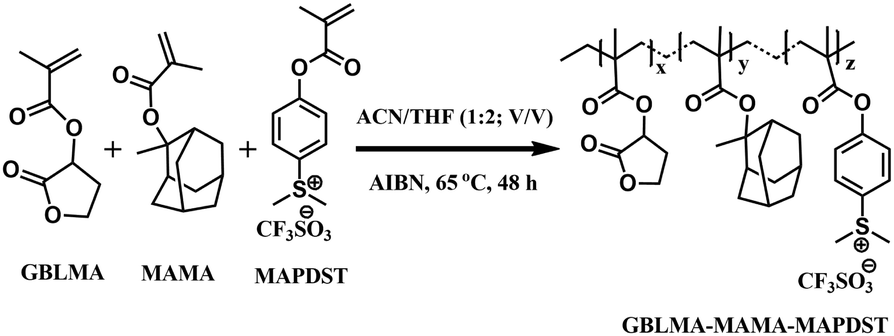
Further, the monomer units present in the GBLMA–MAMA–MAPDST polymer backbone were characterized by NMR analysis. The broad proton resonance peaks at 8.1 and 7.4 ppm were due to the phenyl protons of the MAPDST unit (see, Fig. 1). The peaks for methyl groups on the sulfonium centre were observed at 3.2 ppm.8a The methine (R3C–H) proton of the GBLMA units was located at 5.5 ppm, whereas the peaks due to the –O–CH2– unit of GBLMA appeared at 4.3 and 4.2 ppm. The methyl (–CH3), methylene (–CH2–) and methine (R3C–H) protons of the MAMA units were located at 1.6–2.4 ppm as broad resonance peaks. Moreover, the appearance of broad peaks at 1.5 and 1.0 ppm is due to –CH2– and –CH3 protons of the polymer chain respectively (see, Fig. 1). The fluorine atoms present in the triflate unit (CF3SO3−) of the MAPDST moiety were characterized using 19F NMR spectroscopy and the peak was observed at −77.64 ppm (ESI,† Fig. S5).8 The actual composition of GBLMA, MAMA and MAPDST in the terpolymer GBLMA–MAMA–MAPDST resist was calculated from NMR analysis and found to be 35.22%, 53.4% and 11.36% respectively.
 | ||
| Fig. 1 1H NMR of GBLMA–MAMA–MAPDST resists. | ||
The weight average molecular weight (Mw) of the GBLMA–MAMA–MAPDST polymer was determined using gel permeation chromatography (GPC). Poly(ethyleneglycol) (PEG) and polyethylene oxide (PEO) were used as the standards to plot the size exclusion chromatography (SEC) calibration curve. The calculated molecular weight and polydispersity index (PDI) of the GBLMA–MAMA–MAPDST polymer were found to be 13147 g mol−1 and 3.69 respectively (ESI,† Fig. S6). The thermal stability of the GBLMA–MAMA–MAPDST resist was determined using thermogravimetric analysis (TGA). The polymer was observed to have good thermal stability (stable up to 155 °C), after which it started decomposing with continuous weight loss until 500 °C. The melting temperature of GBLMA–MAMA–MAPDST was analyzed using differential scanning calorimetry (DSC) and found to be 160 °C. The detailed thermal analysis results concluded that the newly developed resist has suitable thermal stability for lithographic applications (ESI,† Fig. S7 and S8).
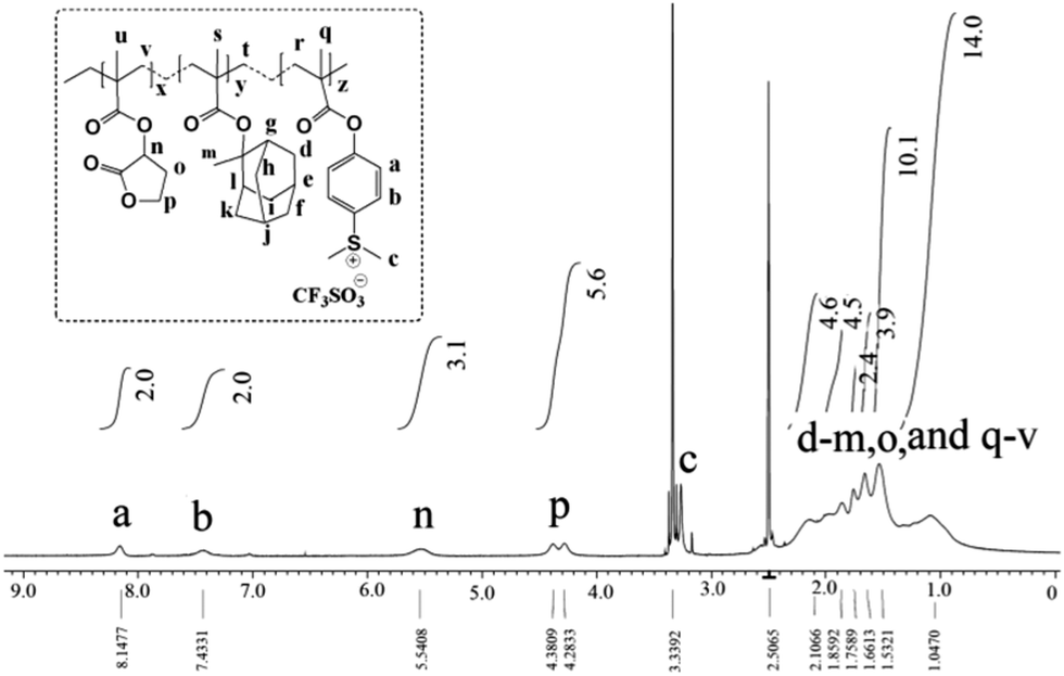
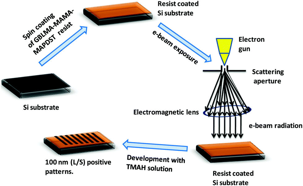
After successful synthesis and complete characterization of GBLMA–MAMA–MAPDST, we examined its application as a positive tone resist material for next generation lithography. RAITH 150-Two was used as an e-beam tool for the lithography studies. The exposure energy and beam current applied for this study were 20 keV and 0.294 nA with a 20 μm aperture respectively. The resist solution was prepared by dissolving GBLMA–MAMA–MAPDST in ethyl lactate solvent (3%; w/v) followed by subsequent double filtration of the resist solution using 0.2 μm Teflon filters in order to remove large size particles from the solution. Thin films were achieved by spin coating of the resist solution onto a 2′′ p-type silicon (100) substrate at a speed of 4500 rpm for 60 s (ESI,† Fig. S9). The excess ethyl lactate present on the silicon substrate was removed by applying a post exposure bake at 130 °C for 60 s. The thin film thickness was calculated using a stylus profilometer and found to be 51 nm (ESI,† Fig. S10). The resist coated thin films were then exposed to various doses of e-beam radiation from 10–80 μC cm−2, followed by applying a post exposure bake at 130 °C for 90 s. The exposed thin films were then developed with the industry standard 0.26 N tetramethyl ammonium hydroxide (TMAH) developer solution for 25 s followed by water rinsing for 10 s. The general lithographic process of the GBLMA–MAMA–MAPDST resist is shown in Fig. 2. The well resolved positive patterns of the GBLMA–MAMA–MAPDST resist with 100 nm L/S and L/2S (line/space) features were obtained at the e-beam exposure dose of 40 μC cm−2 (see, Fig. 3). The line edge roughness (LER) values were calculated for the 100 nm line/space features using a standard metrology analysis tool of the “SUMMIT” package as 2.46 ± 0.33 nm.
 | ||
| Fig. 2 General schematic lithographic processes of the GBLMA–MAMA–MAPDST resist. | ||
 | ||
| Fig. 3 100 nm line patterns of the GBLMA–MAMA–MAPDST resist: (a) SEM image of 100 nm line/space patterns (Mag: 40000×); (b) AFM image of 100 nm L/2S (line/space) features. | ||
The sensitivity curve of the GBLMA–MAMA–MAPDST resist was calculated based on the e-beam exposure dose (20–50 μC cm−2) and absolute thickness (see, Fig. 4). A contrast curve generally provides information about the quality of the resist. The absolute thickness of the GBLMA–MAMA–MAPDST resist depends on the e-beam exposure doses. The e-beam exposure results showed that upon increasing the e-beam dose, the absolute thickness of the resist was decreased indicating its positive tone nature when the patterns are developed in TMAH developer. The contrast (γ) and sensitivity (E0) of the GBLMA–MAMA–MAPDST resist were calculated to be 0.08 and ∼36.5 μC cm−2 respectively, which are much better than those PAG incorporated e-beam resists reported in the literature5e,f (see, Fig. 4). The high sensitivity (36.5 μC cm−2) of GBLMA–MAMA–MAPDST is possibly due to its high PAG content (11.36%).5g,h
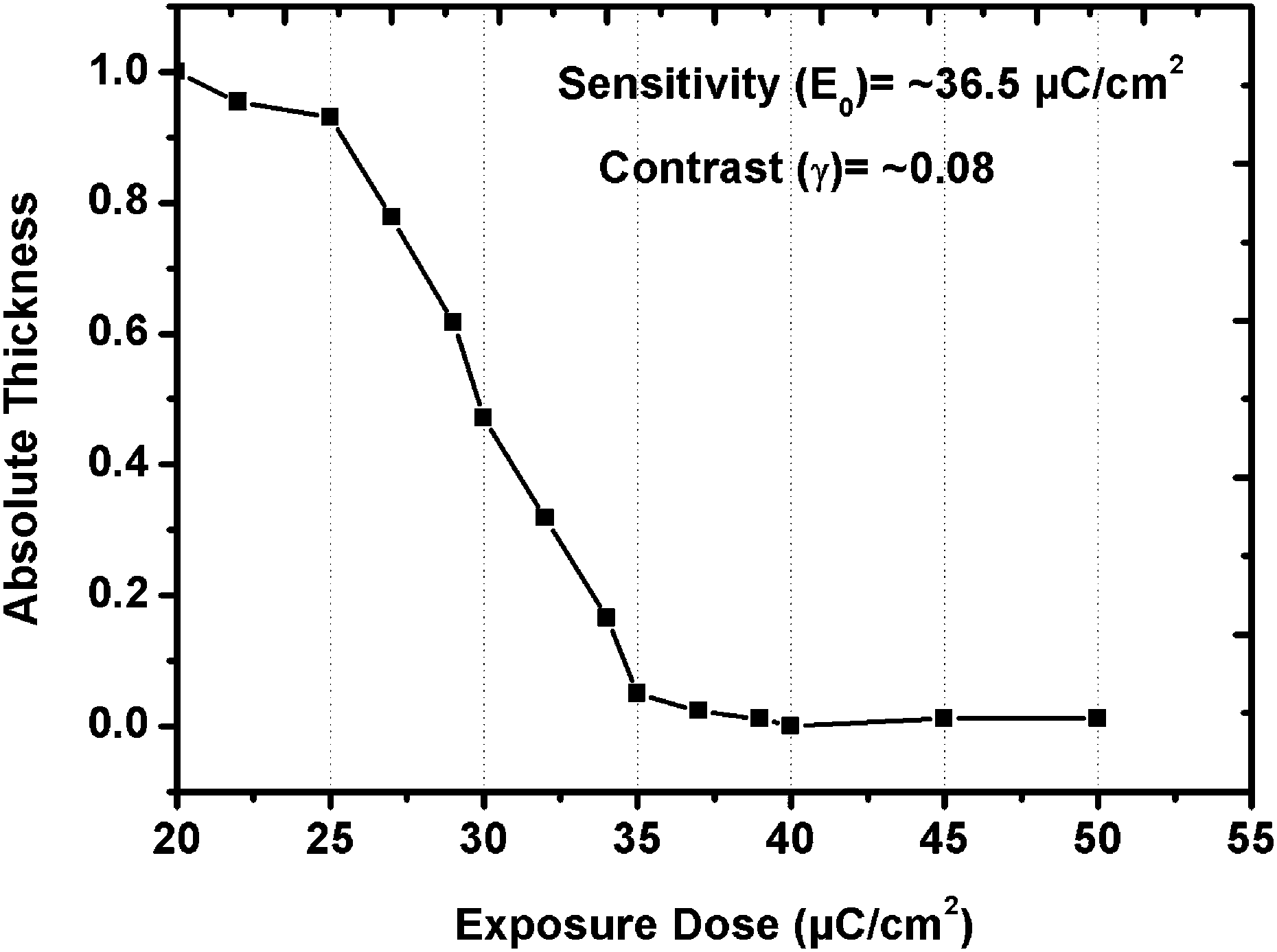 | ||
| Fig. 4 Absolute thickness vs. e-beam exposure dose characteristics of the GBLMA–MAMA–MAPDST resist. | ||
Finally, to evaluate the potential of GBLMA–MAMA–MAPDST in transferring line/space patterns into the silicon substrate, we subjected 100 nm, line/space patterns of poly GBLMA–MAMA–MAPDST resist thin films to a dry plasma etching technique for 15–45 s. AMAT CRUSAR was used as a dry plasma etching tool at 800 W. The etchant used for these studies was SF6 at a flow rate of 100 sscm and pressure of 15 mTorr. Acetone was used to remove the protected resist from the silicon substrate. The thickness of patterned lines was measured before and after plasma etching followed by stripping of the polymer film from the etched silicon substrate (see, Table 1). After the removal of the resist patterns from the silicon etched surface, the thicknesses of the transferred line features were measured to be 107 nm and 423 nm at the etch time of 15 and 45 s respectively (see, Table 1). The corresponding thickness measurements with time are given in the ESI,† Fig. S11 and S12. The higher thickness (∼423 nm) of the transferred line features might be due to the prolonged etching time of the resist silicon substrates with high etchant flow rate and voltage. The etching results revealed that the replicated patterns of the developed photoresist from the mask were successfully transferred into the silicon substrates. These etched patterns of silicon substrates at 100 nm (line/space) characteristics are shown in Fig. 5. Given the potential of this newly developed e-beam resist in transferring high resolution 100 nm half-pitch patterns onto a silicon substrate, one can expect that the GBLMA–MAMA–MAPDST resist may be used for producing ICs for CMOS technology.
| Before etch thickness (nm) | Etch time (seconds) | After etch thickness (nm) | Thickness after the removal of the polymer film from the etched surface (nm) |
|---|---|---|---|
| 46.8 | 15 | 133 | 107 |
| 45 | 45 | 428 | 423 |
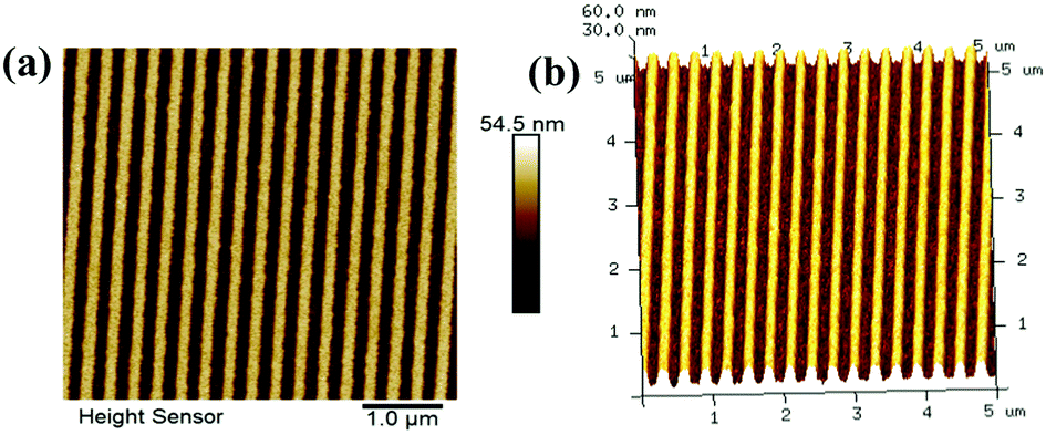 | ||
| Fig. 5 (a) AFM images: (a) 100 nm (line/space) transferred patterns; (b) 3-D view of 100 nm (line/space) transferred patterns. | ||
The designed terpolymer construction was based on three individual monomers, i.e. GBLMA, MAMA and MAPDST, with every structural unit having special characteristics for the resist functioning. The GBLMA unit in the resist structure enhances the adhesive property towards silicon substrates.5a Likewise, the MAMA unit improves the etch resistance property and easily undergoes acid induced polarity conversion by cleaving off the ester functionality.5c Finally, the role of the MAPDST functionality in the resist structure is to produce acids in the solid state for bringing in required chemical changes and also to induce better thermal stability.5c Sulfonium triflates are sensitive and easily undergo photo decomposition when they are exposed to a suitable light source.2e,8 Similarly, upon e-beam irradiation of the poly GBLMA–MAMA–MAPDST resist coated thin films, the counter triflate functionality of sulfonium MAPDST undergoes decomposition to produce strong acids in the solid state. The generated acid catalyzes the cleavage of the ester functionality present in the GBLMA and MAMA units. This emergent structural transformation leads to the solubility difference between the exposed and unexposed regions by changing the polarity of the polymer from an unexposed non-polar region to an exposed polar region. The e-beam exposed hydrophilic portions of the resist structures were developed in TMAH, which led to the positive patterning on the silicon substrate.
Conclusions
To conclude, we have developed one new terpolymer resist (GBLMA–MAMA–MAPDST) bearing PAG as an integrated part of the resist backbone for acid diffusion control and hence to improve pattern sharpness as well as resolution. The resist has been found to be electron beam active and successfully patterned 100 nm line/space features. The sensitivity (36.5 μC cm−2) of this newly developed resist was found to be higher than those reported for PAG incorporated resists. The most interesting feature of this resist is its potential in transferring 100 nm resolution (line/space) patterns onto the silicon substrate through a suitable etching technique. We believe that the present resist will be interesting to those who are working in the area of CMOS and other semiconductor technology.Acknowledgements
AMRC, IIT Mandi is acknowledged for the infrastructural facilities. The authors acknowledge the use of the center of Excellence in Nanoelectronics (CEN) facilitates at IIT Bombay under the Indian Nanoelectronics users program (INUP), India. Financial support received from the Department of Science and Technology, India (Grant No. GITA/DST/TWN/P-69/2015) and Semiconductor Laboratory, Mohali, India (Grant No. SCL/PPED/VFD/IV/022) is thankfully acknowledged.Notes and references
- (a) Y. Xia and G. M. Whitesides, Annu. Rev. Mater. Sci., 1998, 28, 153 CrossRef CAS; (b) K. L. Berkowski, K. N. Plunkett, Q. Yu and J. S. Moore, J. Chem. Educ., 2005, 82, 1365 CrossRef CAS; (c) T. Chen, I. Amin and R. Jordan, Chem. Soc. Rev., 2012, 41, 3280 RSC.
- (a) R. P. Seisyan, Tech. Phys., 2011, 56, 1061 CrossRef CAS; (b) Y. Chen, Microelectron. Eng., 2015, 135, 57 CrossRef CAS; (c) F. Watt, A. A. B. Ettiol, J. A. Vankan, E. J. Teo and M. B. H. Bress, Int. J. Nanosci., 2005, 4, 269 CrossRef CAS; (d) S. Y. Moon and J. Kim, J. Photochem. Photobiol., C, 2007, 8, 157 CAS; (e) S. Ghosh, C. P. Pradeep, S. K. Sharma, P. G. Reddy, S. P. Pal and K. E. Gonsalves, RSC Adv., 2016, 6, 74462 RSC.
- (a) H. Ito, Adv. Polym. Sci., 2005, 172, 37 CrossRef CAS; (b) S. A. M. Donald, C. G. Willson and J. M. J. Frechet, Acc. Chem. Res., 1994, 27, 151 CrossRef; (c) M. D. Stewart, K. Patterson, M. H. Somervell and C. G. Willson, J. Phys. Org. Chem., 2000, 13, 767 CrossRef CAS; (d) E. Reichmanis and L. F. Thompson, Chem. Rev., 1989, 89, 1273 CrossRef CAS.
- (a) J. W. J. Thackeray, J. Micro/Nanolithogr., MEMS, MOEMS, 2011, 10, 033009 CrossRef; (b) P. P. Naulleau, C. N. Anderson, L. M. Baclea-an, P. Denham, S. George, K. A. Goldberg, G. Jones, B. Mc Clinton, R. Miyakawa, S. Rekawa and N. Smith, Proc. SPIE, 2011, 7972, 797202 CrossRef; (c) Y. Wei, M. Bender, W. D. Domke, A. Laessig, M. Sebald, S. Trogisch and D. Back, Proc. SPIE, 2007, 6519, 65190R CrossRef; (d) V. Singh, V. S. V. Satyanarayana, S. K. Sharma, S. Ghosh and K. E. Gonsalves, J. Mater. Chem. C, 2014, 2, 2118 RSC; (e) T. Kolb, C. Neuber, M. Krysak, C. K. Ober and H. W. Schmidt, Adv. Funct. Mater., 2012, 22, 3865 CrossRef CAS.
- (a) M. Wang, N. D. Jarnagin, C. T. Lee, C. L. Henderson, W. Yueh, J. M. Roberts and K. E. Gonsalves, J. Mater. Chem., 2006, 16, 3701 RSC; (b) K. E. Gonsalves, M. Wang, C. T. Lee, W. Yueh, M. T. Tapia, N. Batinad and C. L. Henderson, J. Mater. Chem., 2009, 19, 2797 RSC; (c) M. Wang, C. T. Lee, C. L. Henderson, W. Yueh, J. M. Roberts and K. E. Gonsalves, J. Mater. Chem., 2008, 18, 2704 RSC; (d) M. Wang, K. E. Gonsalves, M. Rabinovich, W. Yueh and J. M. Roberts, J. Mater. Chem., 2007, 17, 1699 RSC; (e) O. Kwon, A. D. Sagar, H. N. Kang, H. M. Kim, K. B. Kim and H. Lee, J. Nanosci. Nanotechnol., 2014, 14, 6270 CrossRef CAS PubMed; (f) K. E. Lee, M. J. Kim, J. B. Yoo, H. S. Mondkar, K. Sohn and H. Lee, J. Nanosci. Nanotechnol., 2012, 12, 725 CrossRef CAS PubMed; (g) C. T. Lee, C. L. Henderson, M. Wang, K. E. Gonsalves, W. Yueh and J. M. Roberts, Microelectron. Eng., 2008, 85, 963–965 CrossRef CAS; (h) M. Thiyagarajan, K. Dean and K. E. Gonsalves, J. Photopolym. Sci. Technol., 2005, 6, 737–741 CrossRef.
- (a) M. Bigas, E. Cabruja, J. Forest and J. Salvi, Microelectron. J., 2006, 37, 433 CrossRef; (b) B. I. Abdulrazzaq, I. A. Halin, S. Kawahito, R. M. Sidek, S. Shafie and N. A. Md. Yunus, SpringerPlus, 2016, 5(434), 1–32 Search PubMed; (c) B. L. Dokić, Eng. Technol. Appl. Sci. Res., 2013, 3, 552 Search PubMed.
- P. M. Gonthier, P. Magnan and F. Corbiere, Proc. SPIE, 2005, 5978, 597812 CrossRef.
- (a) P. G. Reddy, N. Mamidi, P. Kumar, S. K. Sharma, S. Ghosh, K. E. Gonsalves and C. P. Pradeep, RSC Adv., 2016, 6, 67143 RSC; (b) P. G. Reddy, S. P. Pal, P. Kumar, C. P. Pradeep, S. Ghosh, S. K. Sharma and K. E. Gonsalves, ACS Appl. Mater. Interfaces, 2017, 9, 17–21 CrossRef CAS PubMed.
Footnote |
| † Electronic supplementary information (ESI) available. See DOI: 10.1039/c7qm00140a |
| This journal is © the Partner Organisations 2017 |