
Time-dependent transport characteristics of graphene tuned by ferroelectric polarization and interface charge trapping
Wenjing
Jie
 ab and
Jianhua
Hao
*b
ab and
Jianhua
Hao
*b
aCollege of Chemistry and Materials Science, Sichuan Normal University, Chengdu, China
bDepartment of Applied Physics, The Hong Kong Polytechnic University, Hung Hom, Hong Kong. E-mail: jh.hao@polyu.edu.hk
First published on 22nd November 2017
Abstract
Graphene-based field effect transistors (FETs) were fabricated by employing ferroelectric Pb(Mg1/3Nb2/3)O3-PbTiO3 (PMN-PT) as a gate insulator. The co-existing effects of ferroelectric gating and interface charge trapping on the transport properties of graphene were investigated with respect to the FET structure. The sheet resistance (Rs) of graphene shows a slight decay under a small applied voltage, which is much less than the coercive voltage of the ferroelectric PMN-PT, suggesting non-negligible charge trapping effects. Moreover, when the applied voltage is increased up to a value larger than the coercive voltage, Rs exhibits three states: an initial rapid change, followed by a slow nearly exponential evolution, and finally a saturated state either during the applied voltage is retained or after it is released. In particular, a high-resistance state is finally reached due to the ferroelectric gating, implying that ferroelectric effects dominate this process. The underlying physical mechanism was fully investigated to effectively address the observed evolution of time-dependent Rs. Such a finding provides us an opportunity to understand the co-existing effects of ferroelectric gating and charge trapping and tune the transport properties of graphene through the interface effects.
1. Introduction
Graphene, as a new generation material, has been extensively studied based on the field effect transistor (FET) structures by integrating it with traditional SiO2, HfO2, Al2O3 and some other high-k dielectrics.1–3 Among them, ferroelectric materials not only possess a high dielectric constant but also exhibit nonlinear and non-volatile polarization.4 Consequently, graphene has been widely reported to combine with ferroelectric materials in order to achieve attractive properties and realize non-volatile memory device operations.5–11 For example, previous studies on graphene/ferroelectric heterostructures have showed that large-area chemical-vapor-deposited (CVD) graphene could reach a high carrier doping level by organic ferroelectric poly(vinylidene fluoride-co-trifluoroethylene) (PVDF-TrFE) gating,12,13 making graphene show potential for applications in flexible and transparent electrodes to substitute traditional conductive indium tin oxide (ITO). In addition, graphene-based ferroelectric FETs (GFeFETs) by lead zirconate titanate (PZT) gating demonstrated a mobility in excess of 1.5 × 105 cm2 V−1 s−1,9 and a complete conversion of a p-type graphene into n-type through ferroelectric polarization reversal.14 Moreover, a graphene/ferroelectric tunneling junction with ferroelectric BiFeO3 ultra-thin film as a tunnel layer was reported in our recent study to achieve a ultra-high on/off ratio in graphene based FETs.15 Furthermore, the ferroelectric non-volatility and nonlinear polarization can effectively tune the transport properties of the graphene layer and dramatically improve the performance of fabricated devices, such as the non-volatile behaviors used in information storing and hysteresis behaviors in the transport properties.5,16,17 Actually, the interface charge trapping also can induce the hysteresis in the transport behaviors of FETs, not only for graphene but also other two-dimensional (2D) materials, such as MoS2.18–23 Based on some previous studies, there are primarily two factors, which can affect the transport properties of graphene as well as induce the hysteresis in the transport properties of GFeFETs. First, the ferroelectric polarization can manipulate and dramatically tune the transport properties of graphene through the strong interaction between graphene and the ferroelectric gate.23–25 The second factor is the charge trapping and de-trapping at the interface between graphene and gate materials, which can induce large hysteresis in the transport curves and tune the performance of the GFeFETs.25–27 Moreover, the surface adsorbates (e.g., the contaminations, water and oxygen molecules) are found to contribute to the inverse resistance hysteresis, i.e., anti-hysteresis, in the transport properties of GFeFETs. Although some studies have been conducted to separate the intrinsic ferroelectric contributions from the external interaction of surface and/or interface charging and adsorbed molecules,25,26 it appears to be difficult to exclude the effects of such external factors. The behaviors of graphene are not only tuned by the underlying ferroelectric gating but also affected by the interface charge trapping. Hence, it is essential to understand the coupling mechanism between graphene and the ferroelectric gate, as well as the interface charge trapping effects. The charge trapping and de-trapping processes and the impact of such trapped charges on the transport properties of graphene are intrinsically slow evolutions, which can show an appreciable time-dependent profile. However, the time-dependent transport properties of graphene by ferroelectric gating are rarely reported.14,28 Very recently, Lipatov et al. reported a detailed analysis of interplay between the ferroelectric polarization and the interfacial charge traps as well as time-dependent measurements in graphene/PZT FETs.29 However, their study focused on investigating the ferroelectric polarization-dependent electronic transport properties of graphene by minimizing the effect of charge traps. In this study, we employed CVD-grown graphene and ferroelectric Pb(Mg1/3Nb2/3)O3-PbTiO3 (PMN-PT) to investigate the co-existing effects of ferroelectric polarization and charge traps, in contrast to ruling out or minimizing the charge trapping reported in previous studies by other groups. Furthermore, under a gate voltage either smaller or larger than the coercive voltage of the ferroelectric PMN-PT, the time-dependent transport properties exihibted different evolution profiles, suggesting the dominating effects of charge trapping or ferroelectric gating based on our fabricated heterostructures. The strategy of exploring the time-dependent transport properties in this study provides an approach to investigate the co-existing effects of both ferroelectric polarization and charge traps simultaneously.2. Results and discussion
To fabricate GFeFETs, a monolayer of CVD-grown graphene is transferred onto single-crystal ferroelectric PMN-PT substrate. Fig. 1a shows a typical Raman spectrum of a monolayer of CVD-grown graphene with the feature peaks of G and 2D. The peak position and intensity can be achieved by fitting the specific peak with a single-peak Lorentz function. The 2D band exhibits a symmetrical sharp peak with full-width-at-half maximum (FWHM) of about 40 cm−1. The 2D (centered at about 2700 cm−1) band exhibits approximately 2 times the intensity of the G peak (located at about 1580 cm−1), implying that the CVD-grown graphene is a single-layer.30,31 In addition to the two feature bands, there are some rough and broad peaks arising from the underlying PMN-PT substrate. Furthermore, Fig. 1b shows the Raman mapping image of G and 2D bands of the graphene over an area of 4 μm × 4 μm. The mapping image reveals that a uniform and continuous graphene layer has been well transferred onto the PMN-PT substrate. Moreover, the defect-related D peak (located at about 1350 cm−1) is not observed either in the Raman spectrum or in the mapping image, indicating the absence of significant defects and the good quality of the transferred graphene. Then, the source and drain electrodes were prepared by thermal evaporation for the following transport measurements as schematically shown in the inset of Fig. 1a. The device fabrication and characterization are discussed in the Experimental section. Furthermore, monolayer graphene sheets were transferred onto SiO2/Si substrates and graphene/SiO2 FETs are fabricated for comparison.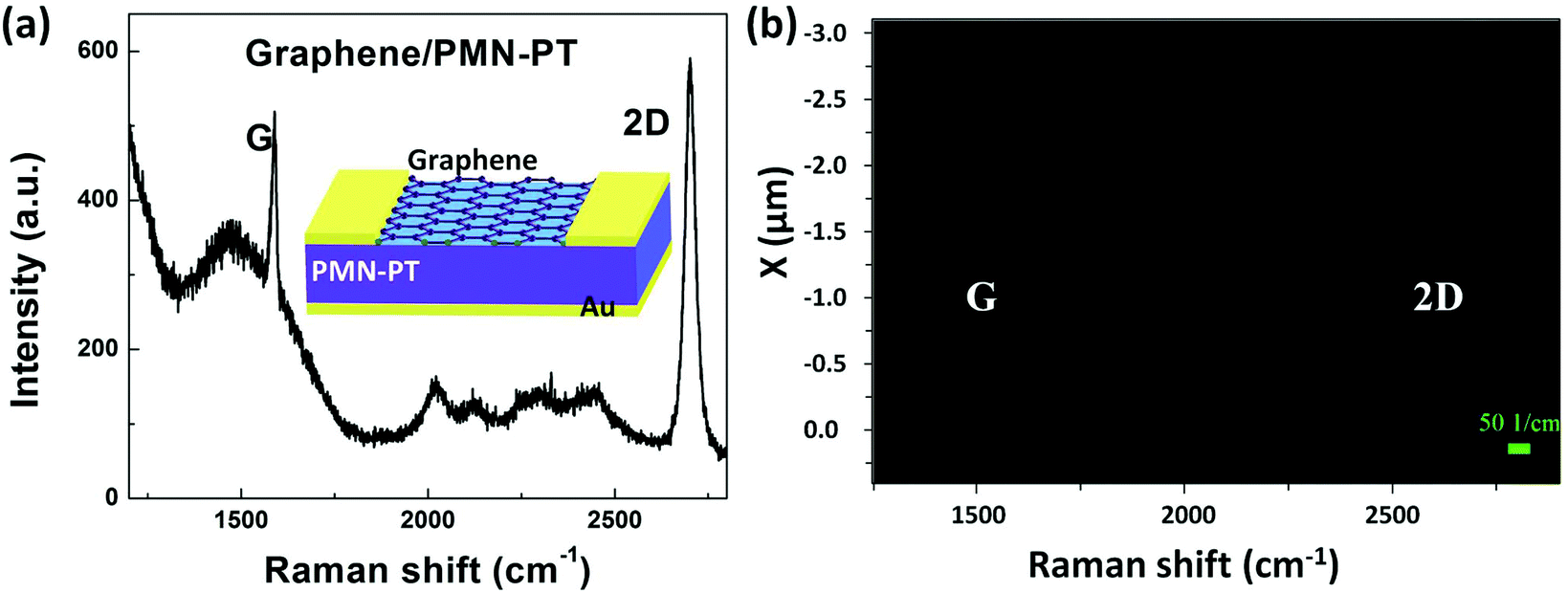 | ||
| Fig. 1 (a) Raman spectrum of graphene on PMN-PT substrate. The inset shows the schematic of graphene/PMN-PT heterostructure. (b) Raman mapping image of the graphene on PMN-PT substrate with the x axis of Raman shift, y axis of Raman mapping scale X and vertical axis of the Raman spectra intensity. | ||
Then, the transport characteristics of the graphene were systematically studied in the GFeFETs by PMN-PT gating. The sheet resistance (Rs) of graphene is calculated by measuring the drain current (Ids) when a source–drain voltage (Vds) of 0.5 V is biased. Fig. 2 shows the Rs of graphene as a function of the gate voltage (Vg). It is observed that the range of applied Vg is gradually increased from 50 to 100 to 150 V as shown in Fig. 2a, b and c, respectively. From Fig. 2a, it is clear that the Rs decreases with backward sweeping Vg, while it increases with forward sweeping, suggesting that the CVD-grown graphene is p-type in air at room-temperature. Moreover, a slight hysteresis loop is observed in the resistance curves. Similar p-type characteristics with an on/off ratio of about 3 can be observed for graphene layers on both PMN-PT and SiO2 when the range of Vg increases up to 100 V as shown in Fig. 2b and d, respectively. A relatively large hysteresis loop is observed in graphene on PMN-PT compared to that on SiO2. It should be pointed out that the charge concentration and resistivity of graphene primarily depend on the dielectric gate materials. To be more specific, the doping concentration is proportional to the dielectric constant of the gating insulator, while varying in inverse ratio to its thickness under the same Vg. Although the room-temperature dielectric constant of PMN-PT (∼5000) is over 3 orders-of-magnitude higher than that of SiO2 (∼3.9), the thickness of PMN-PT (0.5 mm) is over 1000 times higher than that of SiO2 (300 nm). Therefore, it is understandable that the E doping effects on graphene by PMN-PT or SiO2 gating are comparable under identical Vg. Accordingly, Rs of graphene on the PMN-PT is slightly smaller than that on SiO2. For the Vg range up to 150 V, graphene on SiO2 still shows similar transport behaviors. In our experiments, the transport properties of graphene were measured at room-temperature in air ambient. The fabricated FETs exposed to the laboratory environment were always found to be initially p-type due to the adsorbed molecules in air ambient.32 The Dirac point, located at about 130 V, can be observed in graphene/SiO2 FETs when the gate voltage is increased to 150 V as shown in the inset of Fig. 2d. However, for graphene on PMN-PT, the backward and forward scans of Rs show the typical ferroelectric butterfly-shape hysteresis loop when the Vg range is up to 150 V as shown in Fig. 2c. The ferroelectric polarization field in PMN-PT can contribute to the adjacent graphene layer with electrons or holes depending on the applied Vg or polarization direction. As a consequence, the hysteresis in ferroelectric polarization can offset the Dirac point and induce the butterfly-shape hysteresis in Rs of graphene with backward and forward sweeping Vg. Although the fabricated GFeFETs exhibit asymmetry in the hysteresis, reproducible and consistent behaviors are achieved as illustrated in Fig. 2c. This can be caused by some additional doping of water and oxygen from the air as aforementioned. Moreover, in the transport measurements, the Vg was swept from the positive maximum to the negative minimum, and then followed by forward sweeping with a time gap between the backward and forward sweeping. There could be a slight difference in the resistance for backward and forward sweeping due to the nonvolatile ferroelectric polarization; also, the charge trapped at the interface could induce the slight difference in the carrier density as well as the resistance of graphene when Vg is swept in a different direction. Thus, the transport curves are not closed (Fig. 2).
 | ||
| Fig. 2 Sheet resistance of graphene (top panel) on PMN-PT and polarization of PMN-PT crystal (bottom panel) as a function of the gate voltage with the range of (a) 50 V; (b) 100 V; (c) 150 V. (d) Sheet resistance of graphene on SiO2 as a function of the gate voltage with the range of 100 V. The inset shows the transport properties of graphene on SiO2 substrate with the gate voltage up to 150 V. | ||
To further understand the correlation between the transport properties of graphene and ferroelectric polarization of PMN-PT, we measured the hysteresis loop of the polarization (P) versus E from the PMN-PT single crystal with graphene serving as top electrode and Au acting as bottom electrode as shown in Fig. 3a. The P of PMN-PT begins changing at about 75 V (E = 1.5 kV cm−1) and saturates at about 150 V with forward sweeping, while the P remains almost constant until −75 V and saturates at −150 V for backward sweeping with the coercive voltage (Vc) of about ±100 V (coercive field, Ec = 2 kV cm−1). To better understand the measured Rs (Fig. 2), we combined P and Rs dependences on Vg for different Vg scale as shown in Fig. 2a, b and c. In graphene/PMN-PT heterostructure, the ferroelectric P of PMN-PT gradually changes depending on Vg with a slight hysteresis loop. The ferroelectric gating modulates the transport properties of graphene as a conventional dielectric of SiO2 within the Vg regions, where the spontaneous polarization does not reverse, i.e., Vg is less than Vc. The ferroelectric polarization could not be reversed in the Vg range of 50 and 100 V. Herein, the resistance of graphene shows a gradual change when Vg is smaller than the coercive voltage as shown in Fig. 2a and b. As a consequence, the hysteresis loops observed for both devices by PMN-PT or SiO2 gating are primarily a result of the charge trapping at the interface.21,33 Moreover, when Vg exceeds Vc, the polarization can be switched. The simultaneous rise in resistance with the reversal of ferroelectric polarization is expected at Vc (about 100 V), inducing the hysteresis loop in the resistance behaviors when sweeping Vg in forward and backward directions. It is observed that Rs in graphene shows a consistent hysteresis loop with the polarization loop when Vg is beyond Vc. Furthermore, the Hall effect measurement has been performed for the graphene sample on the PMN-PT substrate. The carrier type and density of graphene on PMN-PT substrates under different gate voltage can be obtained as shown in Fig. 3b. The gate voltages in the range of −200 to 200 V with step of 50 V are applied during the measurements. The black circles represent holes, while the blue circles indicate electrons. The red circles stand for the Dirac points. The green arrows stand for the ramping direction of the gate voltage. The CVD-grown monolayer graphene samples exposed to laboratory environment are initially p-type. The excess hole concentration of graphene on PMN-PT under zero gate is measured to be about 5 × 1012 cm−2, which is slightly larger than that of graphene on SiO2 (about 2 × 1012 cm−2). The carrier type is changed into electron when the gate voltage is in excess of 100 V. Similar to the ferroelectric hysteresis in the resistance curve (Fig. 2c), there is a hysteresis in the carrier density of graphene when swithching the gate voltage forward and backward.
 | ||
| Fig. 3 (a) Polarization versus electric field hysteresis loop of PMN-PT. (b) Charge carrier density of graphene on PMN-PT as a function of the gate voltage. The black circles represent hole while blue circles means electron. The red circles mean the Dirac points. The green arrows stand for the ramping direction of gate voltage. (c) Normalized sheet resistance of graphene as a function of gate voltage with different sweeping rates from 1 to 10 V s−1. The green arrows stand for the ramping direction of gate voltage. | ||
Furthermore, it should be noted that the hysteresis direction with the Vg range of 150 V is reversed compared to those with Vg ranges of 50 and 100 V as well as graphene on the SiO2 substrate. Since the interface charge trapping effect dominates the ferroelectric polarization effect, anti-hysteresis can be observed in the transport properties of GFeFETs.14,26,29 Similar transport properties caused by the charge trapping effect have been previously observed even in graphene on conventional dielectric materials, which do not exhibit a spontaneous polarization.21,33 Efforts have been made to eliminate the effect of charge traps on the transport properties of GFeFETs, such as improving the crystalline qualities of the ferroelectric materials or heating the ferroelectric substrates,26 avoiding exposure of GFeFETs to air during the transfer and measurement process,14 or measuring the transport properties after removing the gate voltage.29 In this study, the reverse of anti-hysteresis was realized by the pre-poling the PMN-PT crystal with Vg of −250 V for 10 min prior to the resistance measurements, resulting in the downward polarization state, i.e., the electric dipole moments in the PMN-PT pointing away from the graphene sheet. Then, the anti-hysteresis behaviors can be reversed when the sweeping Vg was larger than the coercive voltage of PMN-PT. This can be caused by the sharp transition of ferroelectric switching of the PMN-PT crystal. The reversed hysteresis suggests that the ferroelectric polarization can dominate the transport properties of graphene under high gate voltage. Moreover, the extrinsic charge trapping effects also can modify the transport properties of graphene. The evidence is that the Dirac points for forward and backward sweeping shift closer to each other when the sweeping rate is changed from 1 to 10 V s−1. Fig. 3b presents the normalized Rs as a function of Vg with different sweeping rates from 1 to 10 V s−1. For fast ramping, the charge trapping effect should be less significant, hence gating should be more effective. The sweeping rate dependent Dirac point shifts are caused from the time-dependent charge trapping or charge distribution effects at the interface. Therefore, the transport behaviors of graphene gating by ferroelectric PMN-PT are tuned by both the underlying ferroelectric polarization and the interface charge trapping. Clearly, the ferroelectric doping is dominated in the transport behaviors of graphene when the Vg range is in excess of the Vc of PMN-PT. Moreover, it should be mentioned that the Dirac points show little variation at the sweeping speeds below 1 V s−1 (not shown here). Actually, not only the Dirac points remain constant but also the transport curves remain unchanged when the sweeping speeds are below 1 V s−1.
To further explore the co-existing effects of ferroelectric polarization and charge trapping, time-dependent Rs was measured under Vg, which is smaller than Vc. In general, the Rs of graphene should remain invariable under a constant E, while graphene on PMN-PT substrate exhibits time-dependent behaviors as shown in Fig. 4a. The pulse signals with the peak-to-peak voltage of 10 V, i.e., from −5 V to +5 V, are used to serve as the Vg. For comparison, we also measured the resistance response of graphene in graphene/SiO2 heterostructures. Both graphene layers are zero biased for more than 1 h until their resistances reach a stable state. Then, gate pulses were applied and the resistances were measured accordingly. Both resistances were modulated at the same frequency as that of the driving signals (10 mHz), and the positive Vg gives rise to the rapid increase of resistance corresponding to the decrease of carrier concentration, while the negative Vg leads to the dramatic decrease in resistance. The observed characteristics are in accordance with the p-type transport properties of graphene. Moreover, there is a slight and negligible change in the resistance during the retention of both positive and negative gate voltages for graphene/SiO2 system caused by the time-dependent interface charge trapping effect. However, the resistance for graphene on PMN-PT shows a gradual evolution under the small Vg, which is much less than Vc. To understand the unique behaviours for graphene on PMN-PT, the surface morphology of the PMN-PT substrate and the as-fabricated graphene were characterized using an atomic force microscope (AFM) (Fig. 4b). It is known that single-crystal PMN-PT possesses a rhombohedral structure and its spontaneous polarization points to the (111)-direction in the pseudo-cubic unit cell.34,35 Thus, some structural kinks inevitably exist at the domain walls, inducing some contrast patterns on the surface of (100)-oriented PMN-PT as shown in the inset of Fig. 4b. Such kinks are also observed in the AFM image of graphene on the top surface of the PMN-PT substrate due to the ultra-thin graphene layer. It was reported that the uneven surface morphology could enhance the charge trapping effects at the interface between the graphene layer and the underlying ferroelectric materials.26 Typically, the charge traps can be divided into two types. One is the surface defects related “intrinsic” traps and the other is the adsorbates related “external” traps. Uneven surface morphology would not only induce more surface defects for the underlying ferroelectric materials but also provide more locations for adsorbates. Thus, we believe that the surface morphology can affect the charge traps at the interface of graphene/PMN-PT. At the rising edge of the gate pulse, Rs increases instantly due to the hole density decrease in graphene caused by the electron accumulation at the interface. Rs then decreases gradually when Vg is maintained at +5 V. In this process, the accumulated electrons at the interface are trapped by the trapping states. As a consequence, the graphene layer gets less gate potential from the underlying ferroelectric gate of PMN-PT. At the falling edge of the gate pulse, Rs decreases rapidly due to the increase in carrier density of holes caused by the hole accumulation at the interface. Rs increases quite slowly during the period of the negative voltage due to the de-trapping process of the trapped electrons. Thus, the carrier density of holes decreases and the resistance increases accordingly.19 By considering that magnitude of the applied gate pulses is much smaller than the coercive voltage, the spontaneous polarization of PMN-PT cannot be switched during the entire process. Herein, the time-dependent behaviors of graphene/PMN-PT are dominated by the charge trapping and de-trapping at the interface when the Vg is much smaller than Vc.
 | ||
| Fig. 4 (a) Sheet resistance of graphene on PMN-PT during the retention of the pulse gate voltages. For reference, sheet resistance of graphene on SiO2 is also shown in the middle panel. Pulse voltages are shown in the bottom panel. (b) AFM image of graphene on PMN-PT. The inset shows the surface morphology of the PMN-PT substrate before graphene transferring. | ||
Moreover, it should be mentioned that single-crystal PMN-PT is also a piezoelectric material possessing a large converse piezoelectric response.36,37 Thus, the Vg not only provides E but also induces in-plane strain, and such strain could be potentially delivered to the above graphene layer.31,38,39 Thus, there could be two possible co-existing tuning mechanisms, i.e., field effect and strain effect with regards to employing PMN-PT as a gate dielectric. The strain provided by the PMN-PT can be calculated according to the change in lattice constant under external E. Actually, the strain is much smaller, typically less than 0.1% for Vg of 500 V.31 However, at least 0.5% strain is required to access the strain dependent resistance.40,41 In addition, typically, a large strain in excess of 20% is needed to induce a band gap in graphene.42,43 Moreover, ohmic contact can be formed between graphene and the electrodes and can be retained even when Vg is up to ±200 V. Accordingly, the effect of piezoelectric strain on the contact resistance can be ignored in our experiments. Therefore, the small piezoelectric strain is negligible in our sample and the strain effects on our GFeFETs can be ruled out, while the ferroelectric field effects and the charge trapping effects are dominant in the transport properties.
By considering that both the reversal of ferroelectric polarization and interface charge trapping can contribute to the observed transport properties in GFeFETs, a large Vg capable of switching the spontaneous polarization in PMN-PT is used in the measurement of time evolution of Rs as illustrated in Fig. 5a. Rs is recorded as a function of time during the retention of a Vg of 200 V, which is sufficiently large to ensure complete switching of the polarization. The time-dependent Rs exhibits three distinct steps when Vg is applied. The initial rapid sharp rise of Rs is followed by a slow exponential increase, and finally, Rs reaches saturation and remains unchanged in the high resistance state after a period of about 100 s. The observed high-resistance state at 200 V can be understood from the initial low-resistance state of p-type properties. Graphene is actually p-doped at zero gated by adsorbates of molecules in air. The ferroelectric spontaneous polarization can further enhance the p-doping properties and contribute to the initial low resistance state. The applied Vg of 200 V is large enough to align the polarization in PMN-PT in the upward direction. By considering the Dirac point located at about 100 V for graphene on PMN-PT, the gate voltage of 200 V can generate electron doping in graphene and the generated electrons can act as current carriers. Moreover, the generated electrons normally “screen” the charge carriers resulting in a weaker “trapping” effect. Due to the time-dependent charge trapping and de-trapping at the interface, a steady exponential increase in resistance is actually observed. When Rs reaches a steady high resistance state, the Vg voltage is removed, and Rs is recorded as a function of time as shown in Fig. 5b. The Rs decreases gradually and reaches a saturation regime after 5000 s. The inset of Fig. 5b shows the log scale data of R(t) − Rh, where R(t) is the time-dependent Rs and Rh stands for Rs at the finally saturated high-resistance state. By considering the unique non-volatility in ferroelectric PMN-PT, the ferroelectric polarization should be retained even when the external field is removed.44 The PMN-PT would finally reach the state with remnant polarization, which can contribute to the high resistance in graphene regardless of the slightly shifted dipoles in PMN-PT. The log scale curve fits well with the red dash line, presenting a linear relationship with time as shown in the inset of Fig. 5b. This presents the exponential decay Rs over time. The initial non-linear or non-exponential change can result from a gradual decrease in the ferroelectric polarization of PMN-PT, while the exponential decay suggests the time-dependent charge injection and trapping at the interface between graphene and PMN-PT. Herein, we can conclude that the Rs evolution exhibits three states, namely an initial rapid change, followed by a slow nearly exponential evolution, and finally a saturated state no matter when the large Vg is retained or after it is released. During the entire process, the transport properties of graphene are tuned by multiple factors, including ferroelectric polarization, non-volatility and charge trapping. However, graphene initially reaches a high-resistance state due to the ferroelectric doping and finally reaches a steady high-resistance state due to the ferroelectric non-volatility from initial retention and subsequent release of Vg. Therefore, the ferroelectric effects are dominated in this process when Vg is larger than Vc.
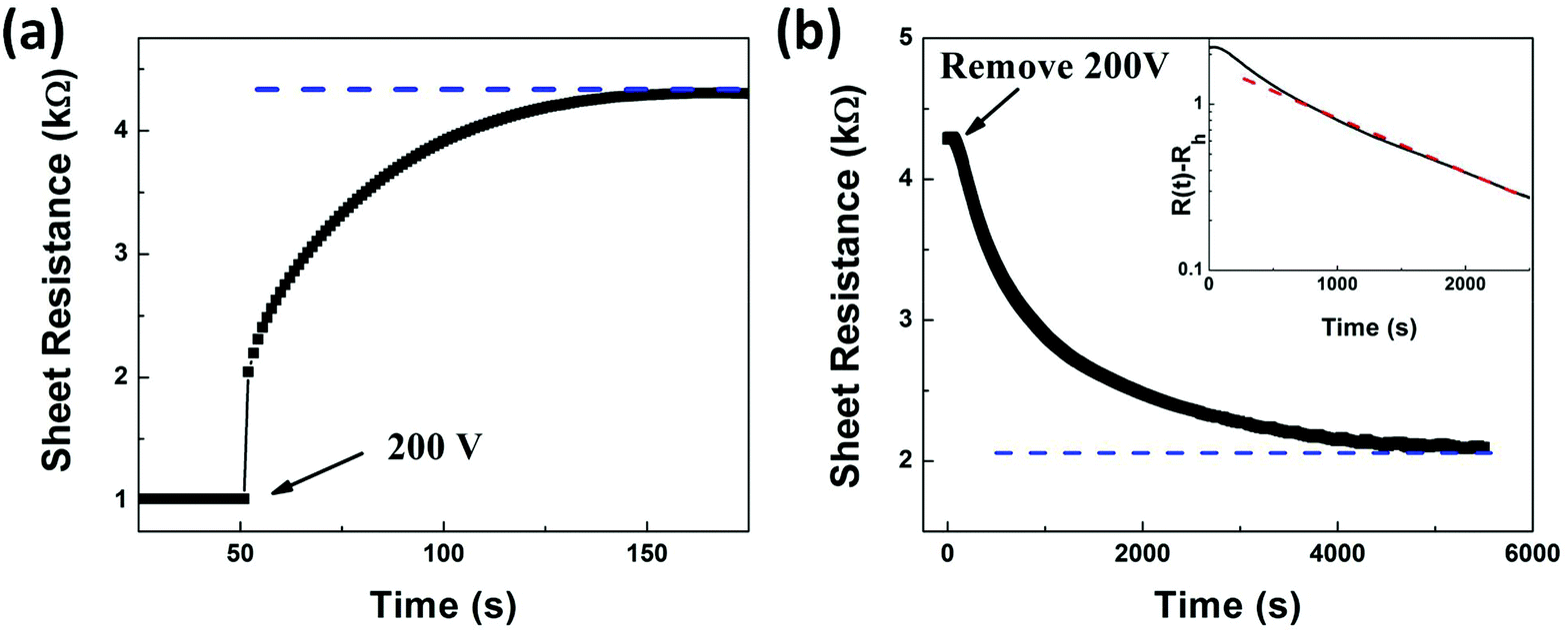 | ||
| Fig. 5 (a) Time-dependent sheet resistance during the retention of a bias voltage of 200 V. (b) Time-dependent sheet resistance after the bias voltage of 200 V is removed. The inset shows the log scale data of R(t) − Rh, where R(t) is the time-dependent sheet resistance and Rh is the final saturated resistance. The log scale curve fits well with the red dash linear line. | ||
3. Experimental
Fabrication of graphene/PMN-PT GFeFETs
Monolayer graphene samples were prepared by CVD method on copper foils and then transferred onto PMN-PT substrates. The detailed growth and transferring methods can be referred to our earlier study.45 After transferring graphene, source and drain electrodes were prepared through a well-designed mask. In our experiments, the electrodes were prepared by first depositing about 15 nm Ti, followed by depositing about 150 nm Au thin films. The Ti buffer layer was used to improve the contact properties between graphene and Au. Good ohmic contact was formed between graphene and the electrodes. Then, Au gate electrodes were directly prepared on the bottom surface of the PMN-PT substrate by sputtering technique. For reference, FETs using traditional SiO2 as gate dielectric were prepared by transferring graphene onto silicon wafers coated with 300 nm thick SiO2.Characterizations
Raman spectroscopy (HORIBA JOBIN YVON, HR800) was employed to examine the CVD-grown monolayer graphene. In the Raman system, the excitation wavelength was 488 nm and 100× objective lens with numerical aperture of 0.9 was provided for the measurements. Atomic force microscopy (AFM, DI Nanocope 8) was used to characterize the surface morphology of the PMN-PT substrate and CVD-grown monolayer graphene after transferring onto the PMN-PT. The carrier density was confirmed by the Hall effect measurement system (Ecopia HMS-3000). The ferroelectric hysteresis loops were measured by the materials measuring system (Premier II, Radiant Technologies Inc., USA). A four-probe technique was employed to measure the transport properties of graphene. In this system, a Keithley 2400 SourceMeter was used to provide a bias voltage of 0.5 V and measure the resistance of graphene. Moreover, a Keithley 2410 was employed to provide the large voltages and a Keithley 3390 Arbitrary Waveform/Function generator was used for the pulse voltage signals. All the above measurements were performed in air at room temperature.4. Conclusions
The co-existing effects of ferroelectric and charge trapping were investigated in graphene/PMN-PT FETs during the retention of Vg and after removing it. It is proposed that the transport properties of graphene are tuned by multiple factors, including ferroelectric polarization, non-volatility and charge trapping during the entire process, in which Vg is retained and subsequently released. Through systematical analysis of the time-dependent transport properties of graphene, we can conclude that Rs shows a slight decay if Vg < Vc due to the charge trapping at the interface. Moreover, if Vg > Vc, Rs evolution exhibits three states: an initial rapid change, followed by a slow nearly exponential evolution and then a saturated state no matter when the large Vg is retained or after it is released. In particular, graphene initially reaches a high-resistance state due to the ferroelectric doping and finally reaches a steady high-resistance state due to the ferroelectric non-volatility. Therefore, the ferroelectric effects are dominated in this process when Vg is larger than Vc.Conflicts of interest
There are no conflicts to declare.Acknowledgements
This work was supported by the grants from Research Grants Council of Hong Kong (GRF No. PolyU 153031/15P), Collaborative Research Fund (CRF No. HKU9/CRF/13G), and National Natural Science Foundation of China (No. 61604100).Notes and references
- A. K. Geim and K. S. Novoselov, Nat. Mater., 2007, 6, 183–191 CrossRef CAS PubMed.
- M. Chhowalla, D. Jena and H. Zhang, Nat. Rev. Mater., 2016, 1, 16052 CrossRef CAS.
- X. Huang, Z. Yin, S. Wu, X. Qi, Q. He, Q. Zhang, Q. Yan, F. Boey and H. Zhang, Small, 2011, 7, 1876–1902 CrossRef CAS PubMed.
- A. Kingon, Nature, 1999, 401, 658–659 CrossRef CAS.
- Y. Zheng, G.-X. Ni, C.-T. Toh, M.-G. Zeng, S.-T. Chen, K. Yao and B. Özyilmaz, Appl. Phys. Lett., 2009, 94, 163505 CrossRef.
- X. Hong, J. Hoffman, A. Posadas, K. Zou, C. H. Ahn and J. Zhu, Appl. Phys. Lett., 2010, 97, 33114 CrossRef.
- E. B. Song, B. Lian, S. M. Kim, S. Lee, T. Chung, M. Wang, C. Zeng, G. Xu, K. Wong, Y. Zhou, H. I. Rasool, D. H. Seo, H. Chung, J. Heo, S. Seo and K. L. Wang, Appl. Phys. Lett., 2011, 99, 42109 CrossRef.
- Y. Zheng, G.-X. Ni, C.-T. Toh, C.-Y. Tan, K. Yao and B. Özyilmaz, Phys. Rev. Lett., 2010, 105, 166602 CrossRef PubMed.
- X. Hong, A. Posadas, K. Zou, C. Ahn and J. Zhu, Phys. Rev. Lett., 2009, 102, 136808 CrossRef CAS PubMed.
- Y. Zheng, G.-X. Ni, S. Bae, C.-X. Cong, O. Kahya, C.-T. Toh, H. R. Kim, D. Im, T. Yu, J. H. Ahn, B. H. Hong and B. Özyilmaz, Europhys. Lett., 2011, 93, 17002 CrossRef.
- S. Raghavan, I. Stolichnov, N. Setter, J. Heron, M. Tosun and A. Kis, Appl. Phys. Lett., 2012, 100, 23507 CrossRef.
- G. Ni, Y. Zheng, S. Bae, C. Tan, O. Kahya, J. Wu, B. H. Hong, K. Yao and B. Özyilmaz, ACS Nano, 2012, 6, 3935–3942 CrossRef CAS PubMed.
- S.-H. Bae, O. Kahya, B. K. Sharma, J. Kwon, H. J. Cho, B. Ozyilmaz and J.-H. Ahn, ACS Nano, 2013, 7, 3130–3138 CrossRef CAS PubMed.
- C. Baeumer, S. Rogers, R. Xu, L. Martin and M. Shim, Nano Lett., 2013, 13, 1693–1698 CrossRef CAS PubMed.
- S. Yuan, Z. Yang, C. Xie, F. Yan, J. Dai, S. P. Lau, H. L. W. Chan and J. Hao, Adv. Mater., 2016, 28, 10048–10054 CrossRef CAS PubMed.
- W. Jie, Y. Y. Hui, N. Y. Chan, Y. Zhang, S. P. Lau and J. Hao, J. Phys. Chem. C, 2013, 117, 13747–13752 CAS.
- W. Jie and J. Hao, Nanoscale, 2014, 6, 6346–6362 RSC.
- S. M. Kim, E. B. Song, S. Lee, J. Zhu, D. H. Seo, M. Mecklenburg, S. Seo and K. L. Wang, ACS Nano, 2012, 6, 7879–7884 CrossRef CAS PubMed.
- Y. Guo, X. Wei, J. Shu, B. Liu, J. Yin, C. Guan, Y. Han, S. Gao and Q. Chen, Appl. Phys. Lett., 2015, 106, 103109 CrossRef.
- M. S. Choi, G.-H. Lee, Y.-J. Yu, D.-Y. Lee, S. H. Lee, P. Kim, J. Hone and W. J. Yoo, Nat. Commun., 2013, 4, 1624 CrossRef PubMed.
- H. Wang, Y. Wu, C. Cong, J. Shang and T. Yu, ACS Nano, 2010, 4, 7221–7228 CrossRef CAS PubMed.
- H. Lu, a. Lipatov, S. Ryu, D. J. Kim, H. Lee, M. Y. Zhuravlev, C. B. Eom, E. Y. Tsymbal, a. Sinitskii and a. Gruverman, Nat. Commun., 2014, 5, 5518 CrossRef CAS PubMed.
- A. N. Morozovska, A. S. Pusenkova, O. V. Varenyk, S. V. Kalinin, E. A. Eliseev and M. V. Strikha, Phys. Rev. B: Condens. Matter Mater. Phys., 2015, 91, 235312 CrossRef.
- N. Park, H. Kang, J. Park, Y. Lee, Y. Yun, J. H. Lee, S. G. Lee, Y. H. Lee and D. Suh, ACS Nano, 2015, 9, 10729–10736 CrossRef CAS PubMed.
- C. Ma, Y. Gong, R. Lu, E. Brown, B. Ma, J. Li and J. Wu, Nanoscale, 2015, 7, 18489–18497 RSC.
- M. H. Yusuf, B. Nielsen, M. Dawber and X. Du, Nano Lett., 2014, 14, 5437–5444 CrossRef CAS PubMed.
- H. Xu, Y. Chen, J. Zhang and H. Zhang, Small, 2012, 8, 2833–2840 CrossRef CAS PubMed.
- S. Raghavan, I. Stolichnov, N. Setter, J. S. Heron, M. Tosun and A. Kis, Appl. Phys. Lett., 2012, 100, 23507 CrossRef.
- A. Lipatov, A. Fursina, T. H. Vo, P. Sharma, A. Gruverman and A. Sinitskii, Adv. Electron. Mater., 2017, 3, 1700020 CrossRef.
- A. C. Ferrari, J. C. Meyer, V. Scardaci, C. Casiraghi, M. Lazzeri, F. Mauri, S. Piscanec, D. Jiang, K. S. Novoselov, S. Roth and a. K. Geim, Phys. Rev. Lett., 2006, 97, 187401 CrossRef CAS PubMed.
- W. Jie, Y. Y. Hui, Y. Zhang, S. P. Lau and J. Hao, Appl. Phys. Lett., 2013, 102, 223112 CrossRef.
- H. Romero, N. Shen and P. Joshi, ACS Nano, 2008, 2, 2037–2044 CrossRef CAS PubMed.
- M. Lafkioti, B. Krauss, T. Lohmann, U. Zschieschang, H. Klauk, K. V. Klitzing and J. H. Smet, Nano Lett., 2010, 10, 1149–1153 CrossRef CAS PubMed.
- T. Nan, M. Liu, W. Ren, Z. G. Ye and N. X. Sun, Sci. Rep., 2014, 4, 5931 CrossRef CAS PubMed.
- T. Wu, P. Zhao, M. Bao, A. Bur, J. L. Hockel, K. Wong, K. P. Mohanchandra, C. S. Lynch and G. P. Carman, J. Appl. Phys., 2011, 109, 124101 CrossRef.
- S. Park and T. R. Shrout, J. Appl. Phys., 1997, 82, 1804–1811 CrossRef CAS.
- Z. Kutnjak, J. Petzelt and R. Blinc, Nature, 2006, 441, 956–959 CrossRef CAS PubMed.
- Y. Y. Hui, X. Liu, W. Jie, N. Y. Chan, J. Hao, Y.-T. Hsu, L.-J. Li, W. Guo and S. P. Lau, ACS Nano, 2013, 7, 7126–7131 CrossRef CAS PubMed.
- F. Ding, H. Ji, Y. Chen, A. Herklotz, K. Dörr, Y. Mei, A. Rastelli and O. G. Schmidt, Nano Lett., 2010, 10, 3453–3458 CrossRef CAS PubMed.
- X.-W. Fu, Z.-M. Liao, J.-X. Zhou, Y.-B. Zhou, H.-C. Wu, R. Zhang, G. Jing, J. Xu, X. Wu, W. Guo and D. Yu, Appl. Phys. Lett., 2011, 99, 213107 CrossRef.
- Y.-H. Lee and Y.-J. Kim, Appl. Phys. Lett., 2012, 101, 83102 CrossRef.
- S.-M. Choi, S.-H. Jhi and Y.-W. Son, Phys. Rev. B: Condens. Matter Mater. Phys., 2010, 81, 081407(R) CrossRef.
- G. Cocco, E. Cadelano and L. Colombo, Phys. Rev. B: Condens. Matter Mater. Phys., 2010, 81, 241412(R) CrossRef.
- Y.-H. Hsieh, F. Xue, T. Yang, H.-J. Liu, Y. Zhu, Y.-C. Chen, Q. Zhan, C.-G. Duan, L.-Q. Chen, Q. He and Y.-H. Chu, Nat. Commun., 2016, 7, 13199 CrossRef CAS PubMed.
- W. Jie, F. Zheng and J. Hao, Appl. Phys. Lett., 2013, 103, 233111 CrossRef.
| This journal is © The Royal Society of Chemistry 2018 |