
Contacts to solution-synthesized SnS nanoribbons: dependence of barrier height on metal work function†
Jenifer R.
Hajzus
 *a,
Adam J.
Biacchi
b,
Son T.
Le
b,
Curt A.
Richter
b,
Angela R.
Hight Walker
b and
Lisa M.
Porter
a
*a,
Adam J.
Biacchi
b,
Son T.
Le
b,
Curt A.
Richter
b,
Angela R.
Hight Walker
b and
Lisa M.
Porter
a
aDepartment of Materials Science and Engineering, Carnegie Mellon University, Pittsburgh, PA 15213, USA. E-mail: jhajzus@andrew.cmu.edu
bEngineering Physics Division, National Institute of Standards and Technology (NIST), Gaithersburg, MD 20899, USA
First published on 30th November 2017
Abstract
Tin(II) monosulfide (SnS) is a layered, anisotropic material that is of interest as a two-dimensional semiconductor for opto-electronic, thermoelectric, and piezoelectric applications. In this study, the effect of work function on contact behavior was investigated. Ni/Au, Pd/Au, Cr/Au, and Ti/Au contacts were fabricated onto individual, solution-synthesized, p-type SnS nanoribbons. The lower work function metals (Cr and Ti) formed Schottky contacts, whereas the higher work function metals (Ni and Pd) formed ohmic or semi-ohmic contacts. Of the ohmic contacts, Ni was found to have a lower contact resistance (∼10−4 Ω cm2 or lower) than Pd (∼10−3 Ω cm2 or lower). Both the calculated Schottky barriers (0.39 and 0.50 eV) for Cr and Ti, respectively, and the ohmic behavior for Ni and Pd agree with behavior predicted by Schottky–Mott theory. The results indicate that high work function metals should be considered to form low resistance contacts to SnS multilayers.
Introduction
The diversity of properties and applications of two-dimensional (2D) materials have vastly expanded since the isolation of graphene1 as additional layered materials have been investigated. For example, phosphorene, recently exfoliated from black phosphorous (BP),2–7 is a p-type semiconductor with a thickness-tunable band gap spanning the energy range between graphene and transition metal dichalcogenides (TMDs).8 Unlike the hexagonal crystal structure of graphene and most TMDs, phosphorene has an orthorhombic “puckered honeycomb” structure leading to intralayer anisotropy in its optical, electronic, mechanical and thermal properties.9 The group-IV monochalcogenides (MX; e.g. M = Sn, Ge; X = S, Se) are a family of layered materials that are isoelectronic with BP. Like BP, their layered structure is buckled, orthorhombic, and anisotropic, but with lower symmetry due to two atomic species. Due to the break in inversion symmetry, IV–VI monolayers are calculated to exhibit significant spin–orbit splitting relevant for spintronics applications10–13 and very large piezoelectricity.14,15 They are predicted to be stable in monolayer form, with micromechanical exfoliation being a viable method for producing single-layered material.16 Additionally, they are expected to be more stable in oxygen-containing environments than phosphorene.17,18 Monolayers of SnSe have been produced by colloidal synthesis19 and by vapor transport followed by N2 etching.20This work focuses on the group-IV monochalcogenide tin sulfide (SnS), which is semiconducting and possesses a thickness-dependent indirect band gap that increases non-monotonically21 from approximately 1.1 eV in bulk22,23 to approximately 2 eV in a monolayer.11,16,21,23–25 It is natively p-type due to the formation of Sn vacancies, which create shallow acceptors.26 Although a few polytypes of SnS are known to exist, the orthorhombic α-SnS (Fig. 1a–c) is considered stable at room temperature;27 it exists naturally in bulk as the mineral herzenbergite. While monolayer SnS has yet to be isolated, bilayer SnS has been synthesized by liquid-phase exfoliation,28,29 and multilayers have been synthesized by physical vapor transport,30,31 mechanical exfoliation,32 and solution methods.33 Interesting properties of SnS monolayers have been proposed such as a high piezoelectric coefficient,15 high thermoelectric figure of merit (ZT),34,35 ferroelectricity,13,36 ferroelasticity,13,37 and valley pairs selectable by linearly polarized light.12,36 SnS monolayer- and thin film-based van der Waals heterojunctions have also been computationally and experimentally investigated,16,29,38–41 and electronic properties of SnS nanoribbons have been calculated.42 Additionally, SnS multilayers have been experimentally demonstrated in transistors31,32 and photodetectors.29,33
 | ||
| Fig. 1 Orthorhombic Pnma crystal structure of α-SnS viewing from the (a) (100) plane, and slightly tilted from the (b) (010), and (c) (001) planes. Lattice constants are a = 1.1180 nm, b = 0.3982 nm, and c = 0.4329 nm.53 SEM images of (d) a solution-synthesized nanoribbon on a SiO2/Si substrate and (e) a high concentration of nanoribbons. | ||
Over the past two decades, SnS has been studied as an earth abundant, non-toxic absorber layer for thin film solar cells as an alternative to copper indium gallium selenide (CIGS) and CdTe.43,44 Bulk SnS has a high absorption coefficient of around 104 cm−1 and a band gap that is close to ideal for photoconversion according to the Shockley–Queisser limit, with calculated efficiencies reaching 24%.45 However, the highest experimental efficiency reported for SnS-based solar cells is 4.36%.46 Resistive losses at the back contact are considered an important loss mechanism in these cells. Highly resistive contacts can also obscure the measurement of intrinsic properties of emerging materials.47,48 High contact resistances can be due to a Schottky barrier height, ΦB, at the metal–semiconductor interface. Schottky–Mott theory states that for a p-type semiconductor, ΦB is equal to the sum of the semiconductor band gap (Eg) and electron affinity (χ) minus the work function of the metal (ΦM). In practice, however, many semiconductors, such as multilayer MoS2,48–50 exhibit a weak dependence of barrier height on metal work function due to Fermi level pinning.
In this work, the electrical behavior of four different metal contacts to individual SnS nanoribbons was investigated. Metals with a range of work functions were selected:51 Ti (ΦM = 4.33 eV), Cr (ΦM = 4.50 eV), Ni (ΦM = 5.15 eV),52 and Pd (ΦM = 5.22 eV). Current–voltage measurements of device structures fabricated using e-beam lithography were used to establish whether the contacts were ohmic or rectifying. Contact resistances and Schottky barrier heights were calculated from the measurements. From the results, a model for band alignments between the metals and SnS is proposed; this model agrees with that predicted based on the Schottky–Mott model and reported properties in the published literature. To the best of the authors’ knowledge, this is the first reported analysis of contact performance on devices fabricated from individual colloidal semiconductor nanocrystals.
Experimental
Device fabrication
Colloidal SnS nanoribbons were synthesized in solution using a procedure described elsewhere (see ESI† for details).54 The resulting semiconductor nanocrystals are several μm in length, but only 20 nm or less in thickness (Fig. 1d,e and ESI, Fig. S1†). Our previous studies indicate that these nanoribbons are phase-pure orthorhombic SnS, with p-type conductivity and a hole concentration estimated to be on the order of 1016 cm−3.54 Diluted SnS nanoribbon dispersions in toluene were spin coated at 314 rad s−1 (3000 rpm) for 30 seconds onto a SiO2/p++Si substrate with Ti/Au fiduciary marks and a Ni/Au ohmic back contact (Fig. 2a). The thermal oxide thickness was 100 nm. Following deposition, excess toluene was evaporated in an oven at 80 °C for 1 minute. Samples were then placed in a 2′′ quartz tube furnace and annealed at 375 °C for 15 minutes in forming gas (5% H2/95% Ar, flow rate 800 sccm). Previous spectroscopic analysis has indicated that annealing under these reducing conditions fully removes residual organics from the surface.54,55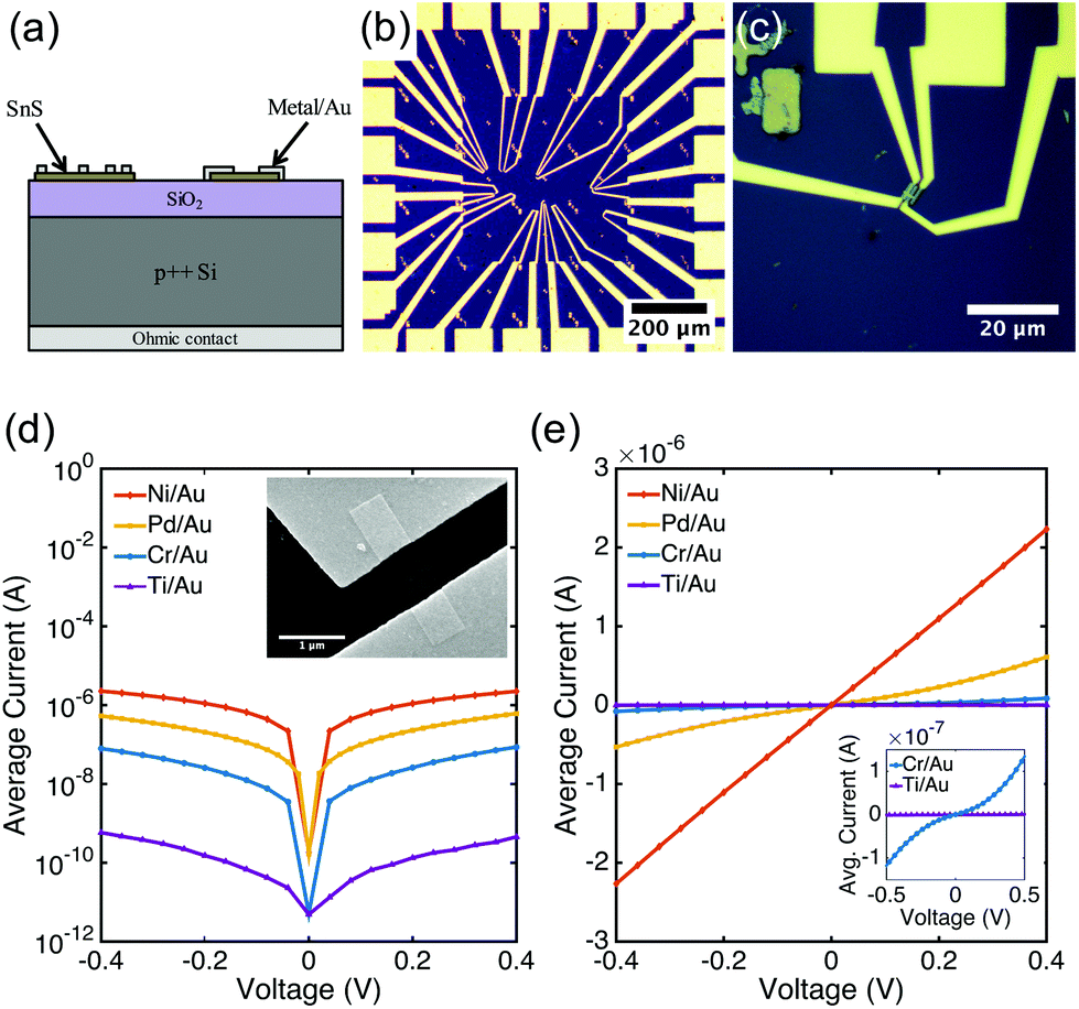 | ||
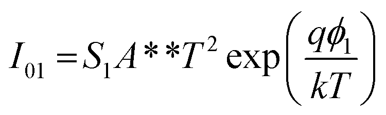
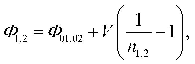
| Fig. 2 (a) Cross sectional schematic of device structure. Two nanoribbons with different contact configurations are shown. (b) Optical microscope image of a sample with many contact test structures patterned in one area and (c) a higher magnification image of a nanoribbon with four contacts. Average I–V sweeps for each contact metallization with 1 μm channel spacing on a (d) log and (e) linear scale, showing ohmic and semi-ohmic behavior for Pd/Au and Ni/Au contacts, and Schottky behavior for Cr/Au and Ti/Au contacts. Inset in (d) is an SEM image of a two contact Ni/Au device. | ||
Contacts were patterned to individual nanoribbons using electron-beam lithography (Zeiss NVision 40 FESEM with Raith Elphy Quantum) (Fig. 2b and ESI, Fig. S2†). Three different contact configurations were used: (1) two large contacts spaced 1 μm apart; (2) three contacts of equivalent length with spacings of 500 nm and 1 μm; and (3) four contacts of equivalent length with spacings of 250 nm, 500 nm, and 1 μm (Fig. 2c). Contact lengths were designed to be either 250 nm or 500 nm.
Prior to metal deposition, samples were dipped in 1% hydrofluoric acid (HF) for 30 s, dipped in deionized water for 30 s, and then blown dry with N2. Samples were immediately (within 5 min to 10 min) loaded into an e-beam evaporation system (Thermionics) with a base pressure in the 10−7 Pa (10−9 Torr) range. All metals were evaporated at a rate of 0.1 nm s−1, as monitored by a quartz crystal microbalance (QCM). For each contact scheme, 40 nm of the selected metal was deposited, followed by 40 nm of Au. The purities of the commercial metal sources were: 99.995% Ni, 99.95% Pd, 99.996% Cr, 99.995% Ti and 99.999% Au. Following evaporation, liftoff was performed in acetone.
Characterization
Electrical measurements were performed in the dark with a Signatone S-1060H-4QR probe station connected to an Agilent HP 4155C semiconductor parameter analyzer with voltage measurement input resistance >1013 Ω. Scanning electron microscope (SEM) micrographs were acquired with either a Phillips XL30 FESEM or Zeiss InVision 40 FESEM and were used to determine contact dimensions and channel lengths (ESI, Fig. S3†). A minimum of 15 pairs of contacts were analyzed for each deposited metal. Diffuse reflectance spectra were collected on dropcast films of SnS nanoribbons with a PerkinElmer Lambda 950 spectrophotometer equipped with a 150 mm integrating sphere.Results and discussion
Current–voltage sweeps were performed between adjacent contact pairs, and results are presented in Fig. 2d and e. The total resistance between contacts decreases from Ti/Au, Cr/Au, Pd/Au, to Ni/Au. Additionally, Schottky behavior was observed for the contact metals with low work functions (Cr and Ti), whereas ohmic or semi-ohmic behavior was exhibited for the contact metals with high work functions (Ni and Pd). These results were consistent for the 15–28 pairs of contacts that were analyzed for each metal. To quantify the electrical behavior of the contacts, measurements were conducted to calculate Schottky barrier heights and specific contact resistances of the Schottky and ohmic contacts, respectively.Schottky barrier height I–V measurement
The Cr and Ti Schottky contact pairs consist of two back-to-back Schottky diodes in series, separated by a SnS channel length. Different methods have been developed to analyze the room temperature I–V behavior of such a configuration.56–58 Here, a method similar to those of Chiquito et al.59 and Nouchi et al.60 is used. The total current through the device is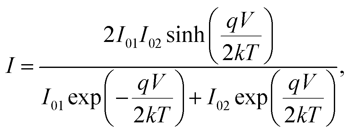 | (1) |
 | (2a) |
 | (2b) |
Ideality factors, n1,2, can be introduced to account for a voltage dependence of the Schottky barrier height.61 The voltage dependence of the barrier height is a consequence of image force lowering, and in some cases an interfacial layer and interface states.61,62 The ideality factor can also increase due to tunneling through the barrier or carrier recombination in the depletion region. A characteristic energy, E00, was calculated to determine the conduction mechanism at the interface.63 When E00 is much smaller than the thermal energy (kT), thermionic emission is expected.64 Room temperature tunneling is not expected in forward bias at these doping concentrations, as E00 ≈ 0.7 meV (calculated using a dielectric constant of 32.814,65,66 and hole effective mass of 0.23m0![[thin space (1/6-em)]](https://www.rsc.org/images/entities/char_2009.gif) 21,23,67). However, tunneling and image force lowering may have a greater impact in reverse bias.61,63 Additionally, there have been reports of larger tunneling contributions for very thin nanostructures.48,68 Taking into account the ideality factor, the modified barrier height is written as,59,61
21,23,67). However, tunneling and image force lowering may have a greater impact in reverse bias.61,63 Additionally, there have been reports of larger tunneling contributions for very thin nanostructures.48,68 Taking into account the ideality factor, the modified barrier height is written as,59,61
 | (3) |
The I–V curves were fit to eqn (1)–(3) using a nonlinear least squares method. The Richardson's constant used was 27.6 A cm−2 K−2, which was calculated with literature values for the bulk SnS hole effective mass in the zigzag direction.21,23,67 It was found that the value used for Richardson's constant did not greatly impact the extracted fit parameters.
Example fits for Cr/Au and Ti/Au back-to-back Schottky contacts are shown in Fig. 3a and b. As indicated by the fit parameters listed in Table 1, the calculated average Schottky barrier heights at the interface with SnS nanoribbons were 0.39 eV and 0.50 eV for Cr/Au and Ti/Au, respectively. These values are in close agreement with the values (ΦB,Cr = 0.38 eV and ΦB,Ti = 0.55 eV) predicted by the Schottky–Mott metal–semiconductor band alignment model (Fig. 3c). The electron affinity listed is a reported value for the (100) surface of bulk SnS.69 The band gap of bulk SnS has been reported to be 1.08 eV (ref. 70) and confirmed experimentally using diffuse reflectance spectroscopy (ESI, Fig. S4†).71
 | ||
| Fig. 3 Example fits of I–V sweeps to the back-to-back Schottky diode equation for (a) Cr/Au contacts on SnS and (b) Ti/Au contacts on SnS. I–V sweeps were measured between adjacent contacts. (c) Schottky–Mott band alignment of metals and SnS. χ is the electron affinity of SnS, Eg is the band gap, Evac is the vacuum level, EC is the conduction band minimum, and EV is the valence band maximum. (d) Experimental band alignment. | ||
| Metal | Φ B (eV) | n | R 2 | No. devices |
|---|---|---|---|---|
| Cr/Au | 0.39 ± 0.05 | 1.12 ± 0.02 | 0.996 ± 0.002 | 20 |
| Ti/Au | 0.50 ± 0.06 | 1.13 ± 0.07 | 0.996 ± 0.003 | 15 |
The experimentally determined alignment is depicted in Fig. 3d; the alignments of the ohmic contacts are assumed to be near or below the valence band maximum. The results indicate a lack of Fermi-level pinning and agree with a recent report of ohmic Ni contacts on 50 nm to 100 nm thick multilayer 2D SnS.32 Additionally, an older study reports Ag Schottky contacts to the (100) plane of bulk SnS with a barrier height of 0.649 eV.72 Although the work function of metals can vary depending on orientation and processing, this barrier height value is close to the 0.62 eV value predicted here for polycrystalline Ag (ΦM = 4.26 eV).73
While ideality factors are low, they are higher than those expected for only image force lowering at this moderate doping concentration. This suggests an additional contribution to the ideality factor, such as from tunneling or an interfacial layer. SnS is known to form a thin native oxide at its surface,74 which we have observed previously using X-ray photoelectron spectroscopy.55 The oxide can be removed under reducing conditions but regrows upon exposure to ambient air. While samples were dipped in HF prior to metal deposition, further study is needed to determine the effect this may have on the oxide layer. There have been reports of oxide layers impacting Schottky barrier heights to MoS2.75–78
Specific contact resistance measurement
The specific contact resistance was measured for the ohmic Ni/Au and semi-ohmic Pd/Au contacts. For bulk semiconductors, the specific contact resistance can be measured by a transfer length method (TLM), involving four or more contacts with varying spacings. Due to the confined lengths of the nanoribbons, some were too small for a four contact TLM pattern. For those nanostructures, three contacts were patterned, and a contact end resistance (CER)79 measurement combined with a three-probe contact front resistance measurement were used.64The current in a metal–semiconductor contact encounters two competing resistances- the semiconductor sheet resistance, Rsh, and an interfacial resistance, which is experimentally quantified by the specific contact resistance, ρc. The interface is described by a transmission line model represented in Fig. 4a79,80 The voltage distribution under the contact as a function of distance is given by,79
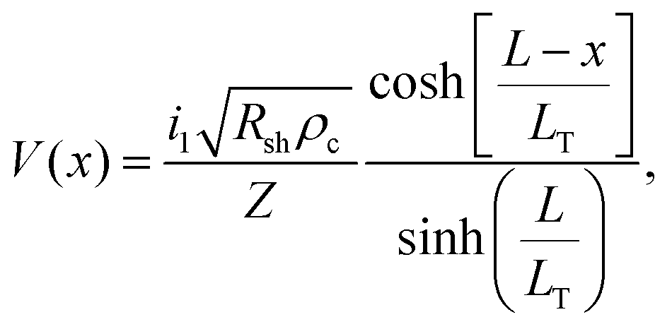 | (4) |
 | (5) |
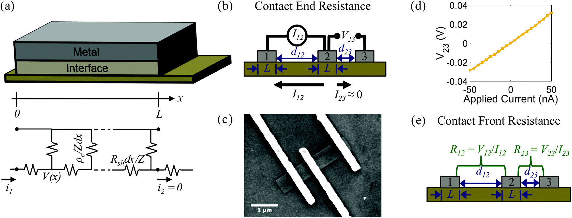 | ||
| Fig. 4 (a) Transmission line model for metal–semiconductor contact. (b) Schematic of contact end resistance measurement. (c) SEM image of a CER structure for Ni/Au contacts on a SnS nanoribbon. (d) Example measurement of V23 for contact end resistance measurement of a set of Pd/Au contacts. (e) Schematic of contact front resistance measurement. | ||
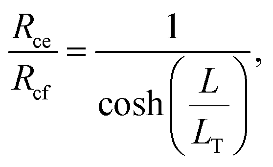
For long contacts (L > 3LT), eqn (4) can be approximated as an exponential function and LT is the distance under the contact in which 1 − (1/e) of the current has entered the metal.
Contact end resistance
The measurement configuration for the CER method is depicted in Fig. 4b. Here, three contacts with equal L and unequal spacings between contacts, d, were fabricated on single nanoribbons (Fig. 4c). Current, I12, was applied between contacts 1 and 2, and voltage, V23, was measured between contacts 2 and 3 (Fig. 4d). The current flowing between contacts 2 and 3 is negligible when a high impedance voltage measurement unit is used. Therefore, this configuration provides a voltage sampling at the end of the contact (i.e., at x = L). From eqn (4) and (5), the contact end resistance, Rce, is given as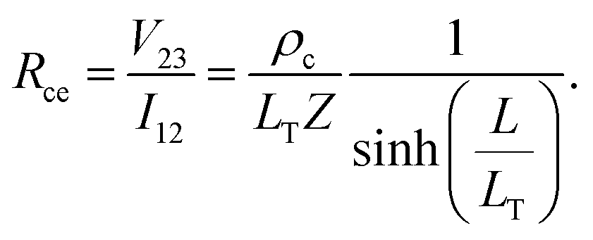 | (6) |
Alternatively, when current, I12, is measured between contacts 1 and 2, and voltage, V12 is applied between contacts 1 and 2, the voltage is sampled at the front of the contact (i.e., at x = 0). From eqn (4) and (5), the contact front resistance, Rcf, can be written as
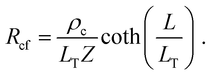 | (7) |
R cf was determined as shown in Fig. 4e, where the total resistance between contacts 1 and 2 (R12), and between 2 and 3 (R23) were measured. The total resistance is64
 | (8) |
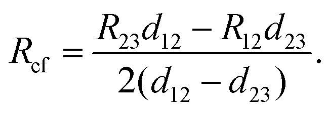 | (9) |
The transfer length was determined by taking the ratio of the contact end and front resistances,
 | (10) |
The results of these measurements are displayed in Table 2. It can be seen that the calculated specific contact resistances of the Pd/Au contacts are higher than those of Ni/Au. The extracted transfer lengths were in most cases approximately equal to the length of the contacts or smaller, and in only a few cases, slightly longer. It was found that the calculated specific contact resistances of devices with transfer lengths longer than the contact were similar to those with shorter transfer lengths. The long transfer lengths will be discussed in terms of the transmission line model in the next section.
| Metal | R cf (Ω) | R ce (Ω) | L (nm) | L T (nm) | R sh (Ω □−1) | ρ c (Ω cm2) |
|---|---|---|---|---|---|---|
| Ni/Au | 4.3 (±3.2) × 104 | 2.8 (±2.2) × 104 | 3.7 (±0.7) × 102 | 3.5 (±0.4) × 102 | 6.1 (±4.9) × 104 | 5.4 (±3.9) × 10−5 |
| Pd/Au | 2.5 (±1.3) × 106 | 7.3 (±1.1) × 105 | 2.8 (±0.2) × 102 | 2.2 (±1.2) × 102 | 7.9 (±7.1) × 106 | 1.3 (±0.3) × 10−3 |
The measured sheet resistance is lower for Ni/Au contacts than Pd/Au contacts. In this method, the extracted sheet resistance is the sheet resistance of the nanoribbon underneath the contact region. A few factors could alter the nanoribbon sheet resistance under the contact, such as a reaction at the interface (Pd and Ni are both thermodynamically predicted to react with SnS81,82), or a depletion width on the order of the thickness (the depletion width is on the order of a few hundred nanometers at this doping density). The variation in sheet resistance and contact resistance values may be a result of different amounts of reactions at the interface between devices.
Transfer length method (TLM)
For longer nanoribbons, a TLM design was patterned, consisting of four contacts on a single nanoribbon. The four contacts of equal length were separated by varying channel spacings, d. The total resistance, RT, was measured between each set of adjacent contacts and is equal to the sum of the resistance contribution from the semiconductor, (Rshd)/Z, and the two contact resistances, 2Rcf. When RT is plotted as a function of d, the y-intercept corresponds to the resistance contribution from the two contacts only and is equal to 2Rcf. Rsh can be determined from the slope, and LT can be determined by extrapolating the x-intercept.64,83 Typically, this method makes use of the approximation that when L ≥ 3LT, the coth(L/LT) term in eqn (7) is approximately equal to 1, and therefore the x-intercept is equal to −2LT. However, Table 2 indicates that L ≥ 3LT is not valid for the geometries here, so this approximation cannot be used. Therefore, the full eqn (7) was used, yielding a total resistance: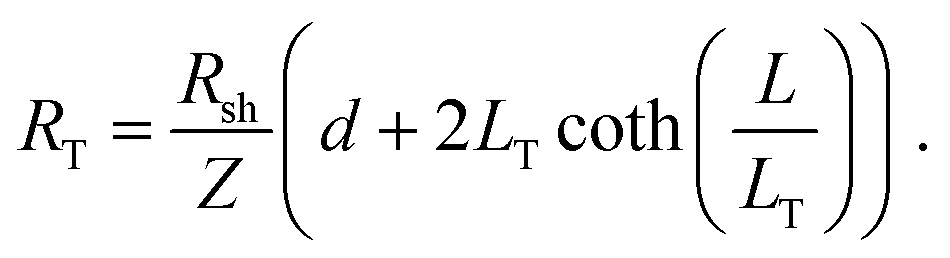 | (11) |
In this case, the x-intercept is equal to −2LT coth(L/LT), and the y-intercept and slope remain equal to 2Rcf and Rsh/Z, respectively. A similar expression was derived for contacts to semiconductor nanowires with short contact lengths.84
The specific contact resistance can also be written in terms of the contact resistance multiplied by the area of the contact. For long contacts (L > 3LT), the transfer length is used for the length, and, from eqn (7), Rcf ≈ ρc/(LTZ).64 For very short contacts, Rcf ≈ ρc/(LZ).64 For the intermediate contact lengths here, neither approximation can be used, but an effective length can be defined, such that
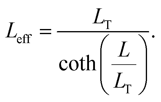 | (12) |
Then, Rcf = ρc/(LeffZ), eqn (4) is derived for a terminal contact, in which all current is collected between x = 0 and x = L such that i2 in Fig. 4a is equal to zero.79 When the contact length becomes less than 3LT, Rcf begins to increase. i1Rcf multiplied by Leff is equal to the integral of the voltage along the entire contact, such that 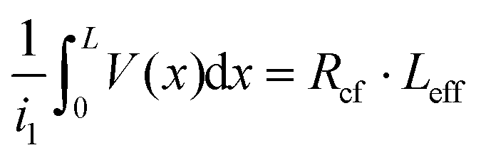 . The specific contact resistance can therefore be calculated by multiplying the measured Rcf by the contact width and effective length, or by solving for ρc in eqn (5) (ρc = LT2·Rsh). This approach assumes all current is collected within the length of the contact and does not take into account spreading resistance beyond the length of the contact.
Plots of RTvs. d are displayed in Fig. 5, and Table 3 lists extracted parameters. Similar to the results extracted by the CER method, it is observed that the specific contact resistance of Ni is lower than that of Pd, and the extracted sheet resistance for Ni is lower than that of Pd. In this case, the transfer length for the Ni/Au contact is larger than the length of the contact, and the transfer length of Pd/Au was greater than L/3. As previously discussed, the specific contact resistances can be calculated using Rcf = ρc/(LeffZ), which are equivalent to the ρc calculated by eqn (5) and (11). Since Rcf will increase with decreasing contact length when the contact length is less than 3LT, this indicates that in devices, a contact length longer than those used here would be ideal to further reduce Rcf.
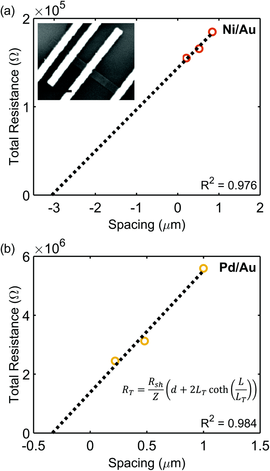 | ||
| Fig. 5 Transfer length method (TLM) plots for extracting sheet resistance, specific contact resistance, and transfer lengths of contacts on an individual SnS nanoribbon for (a) Ni/Au contacts and (b) Pd/Au contacts. Inset in (a) is an SEM image of a representative TLM device. | ||
| Metal | R 2 | R cf (Ω) | L (nm) | L T (nm) | L eff (nm) | R sh (Ω □−1) | ρ c (Ω cm2) |
|---|---|---|---|---|---|---|---|
| Ni/Au | 0.976 | 7.2 (±0.2) × 104 | 2.9 × 10² | 6.4 (±0.5) × 102 | 2.7 (±0.3) × 102 | 2.7 (±0.4) × 104 | 1.1 (±0.3) × 10−4 |
| Pd/Au | 0.984 | 6.9 (±1.7) × 105 | 3.0 × 10² | 1.6 (±0.5) × 102 | 1.5 (±0.5) × 102 | 2.3 (±0.3) × 106 | 5.9 (±3.6) × 10−4 |
The TLM assumes the sheet resistance under the contact is equal to the nanoribbon sheet resistance in the channel. In reality, this may not be the case due to factors such as reactions at the interface or the depletion width being on the order of the thickness of the semiconductor.85 An additional measurement of Rce can take into account a change in underlying Rsh.85,86 The contact end resistance measurement was performed on the Ni/Au TLM structure, and, in conjunction with Rcf determined by the TLM measurement, specific contact resistance parameters were extracted. The sheet resistance determined by incorporating this additional measurement was 3.3 × 10³ Ω □−1, which is lower than that measured by the TLM method alone (2.7 × 10⁴ Ω □−1). This suggests the sheet resistance in the SnS region underneath the Ni/Au contact is lower than the sheet resistance of the pristine SnS channel and therefore may indicate a reaction occurred at the Ni/SnS interface. Further studies would be required to determine the exact nature of the Ni/SnS interface. Possible reaction products of bulk SnS and Ni calculated from FactSage®81 include Ni3Sn2 and Ni3S2. It is interesting to note that the work function of Ni3S2 has been reported to be ∼5 eV,87,88 which is similar to that of unreacted Ni; whereas the work function of Ni3Sn2 may be as low as 4.55 eV.89 Regardless of whether a reaction has occurred at this interface, Ni contacts to SnS nanoribbons appear to behave as predicted by the Schottky–Mott model for a high work function metal.
Conclusion
In this work, Ni, Pd, Cr, and Ti contact test structures were fabricated onto individual, solution-synthesized, p-type SnS nanoribbons. We conducted what we believe to be the first reported analysis of contact performance in devices fabricated from colloidal nanocrystals. The high work function metals (Ni and Pd) formed ohmic or semi-ohmic contacts to SnS nanoribbons, while the lower work function metals (Cr and Ti) formed Schottky contacts. The Schottky barrier heights calculated for Cr and Ti agree well with the band alignment predicted by Schottky–Mott theory, whereas the ohmic behavior of Ni and Pd also agree with the expectations from this model. Of the two ohmic metals, a lower specific contact resistance (on the order of 10−4 Ω cm2 or lower) was consistently calculated for Ni. The results of this study indicate a lack of Fermi level pinning in metal–SnS nanoribbon structures and can inform the selection of contact metals in the design of future SnS-based devices.Conflicts of interest
The authors declare no competing financial interest. Certain commercial equipment or materials are identified in this paper to adequately specify the experimental procedures. In no case does the identification imply recommendation or endorsement by NIST, nor does it imply that the materials or equipment identified are necessarily the best available for the purpose.Acknowledgements
The authors acknowledge the support of the Bertucci Graduate Fellowship at Carnegie Mellon University (J. R. H.), the NIST Director's Fellow Postdoctoral Research Associateship program (A. J. B.) and NIST-STRS for funding. The authors also acknowledge use of the Materials Characterization Facility at Carnegie Mellon University supported by grant MCF-677785. Research was performed in part at the NIST Center for Nanoscale Science and Technology with support from a CNST-UMD Collaboration Travel Grant. We thank Kerry Siebein for her assistance with characterization and fabrication and Yi Luo for valuable discussions. A. J. B. gratefully acknowledges emeritus NIST fellow Herbert Bennett.References
- K. S. Novoselov, A. K. Geim, S. V. Morozov, D. Jiang, Y. Zhang, S. V. Dubonos, I. V. Grigorieva and A. A. Firsov, Science, 2004, 306, 666–669 CrossRef CAS PubMed.
- L. K. Li, Y. J. Yu, G. J. Ye, Q. Q. Ge, X. D. Ou, H. Wu, D. L. Feng, X. H. Chen and Y. B. Zhang, Nat. Nanotechnol., 2014, 9, 372–377 CrossRef CAS PubMed.
- A. Castellanos-Gomez, L. Vicarelli, E. Prada, J. O. Island, K. L. Narasimha-Acharya, S. I. Blanter, D. J. Groenendijk, M. Buscema, G. A. Steele, J. V. Alvarez, H. W. Zandbergen, J. J. Palacios and H. S. J. van der Zant, 2D Mater., 2014, 1, 025001 CrossRef.
- S. P. Koenig, R. A. Doganov, H. Schmidt, A. H. C. Neto and B. Ozyilmaz, Appl. Phys. Lett., 2014, 104, 103106 CrossRef.
- F. N. Xia, H. Wang and Y. C. Jia, Nat. Commun., 2014, 5, 4458 CAS.
- J. S. Qiao, X. H. Kong, Z. X. Hu, F. Yang and W. Ji, Nat. Commun., 2014, 5, 4475 CAS.
- H. Liu, A. T. Neal, Z. Zhu, Z. Luo, X. F. Xu, D. Tomanek and P. D. D. Ye, ACS Nano, 2014, 8, 4033–4041 CrossRef CAS PubMed.
- A. H. Woomer, T. W. Farnsworth, J. Hu, R. A. Wells, C. L. Donley and S. C. Warren, ACS Nano, 2015, 9, 8869–8884 CrossRef CAS PubMed.
- X. Ling, H. Wang, S. X. Huang, F. N. Xia and M. S. Dresselhaus, Proc. Natl. Acad. Sci. U. S. A., 2015, 112, 4523–4530 CrossRef CAS PubMed.
- K. S. Novoselov, A. Mishchenko, A. Carvalho and A. H. C. Neto, Science, 2016, 353, aac9439 CrossRef CAS PubMed.
- L. C. Gomes and A. Carvalho, Phys. Rev. B: Condens. Matter Mater. Phys., 2015, 92, 085406 CrossRef.
- A. S. Rodin, L. C. Gomes, A. Carvalho and A. H. C. Neto, Phys. Rev. B, 2016, 93, 045431 CrossRef.
- M. H. Wu and X. C. Zeng, Nano Lett., 2016, 16, 3236–3241 CrossRef CAS PubMed.
- L. C. Gomes, A. Carvalho and A. H. C. Neto, Phys. Rev. B: Condens. Matter Mater. Phys., 2015, 92, 214103 CrossRef.
- R. Fei, W. Li, J. Li and L. Yang, Appl. Phys. Lett., 2015, 107, 173104 CrossRef.
- A. K. Singh and R. G. Hennig, Appl. Phys. Lett., 2014, 105, 042103 CrossRef.
- L. C. Gomes, A. Carvalho and A. H. C. Neto, Phys. Rev. B, 2016, 94, 054103 CrossRef.
- Y. Guo, S. Zhou, Y. Z. Bai and J. J. Zhao, ACS Appl. Mater. Interfaces, 2017, 9, 12013–12020 CAS.
- L. Li, Z. Chen, Y. Hu, X. W. Wang, T. Zhang, W. Chen and Q. B. Wang, J. Am. Chem. Soc., 2013, 135, 1213–1216 CrossRef CAS PubMed.
- J. Z. Jiang, C. P. Y. Wong, J. Zou, S. S. Li, Q. X. Wang, J. Y. Chen, D. Y. Qi, H. Y. Wang, G. Eda, D. H. C. Chua, Y. M. Shi, W. J. Zhang and A. T. S. Wee, 2D Mater., 2017, 4, 021026 CrossRef.
- C. Xin, J. X. Zheng, Y. T. Su, S. K. Li, B. K. Zhang, Y. C. Feng and F. Pan, J. Phys. Chem. C, 2016, 120, 22663–22669 CAS.
- G. Valiukonis, D. A. Guseinova, G. Krivaite and A. Sileika, Phys. Status Solidi B, 1986, 135, 299–307 CrossRef CAS.
- G. A. Tritsaris, B. D. Malone and E. Kaxiras, J. Appl. Phys., 2013, 113, 233507 CrossRef.
- L. Huang, F. G. Wu and J. B. Li, J. Chem. Phys., 2016, 144, 114708 CrossRef PubMed.
- C. Chowdhury, S. Karmakar and A. Datta, J. Phys. Chem. C, 2017, 121, 7615–7624 Search PubMed.
- J. Vidal, S. Lany, M. d'Avezac, A. Zunger, A. Zakutayev, J. Francis and J. Tate, Appl. Phys. Lett., 2012, 100, 032104 CrossRef.
- L. A. Burton and A. Walsh, J. Phys. Chem. C, 2012, 116, 24262–24267 CAS.
- J. R. Brent, D. J. Lewis, T. Lorenz, E. A. Lewis, N. Savjani, S. J. Haigh, G. Seifert, B. Derby and P. O'Brien, J. Am. Chem. Soc., 2015, 137, 12689–12696 CrossRef CAS PubMed.
- Z. Y. Jia, S. L. Li, J. Y. Xiang, F. S. Wen, X. Bao, S. H. Feng, R. L. Yang and Z. Y. Liu, Nanoscale, 2017, 9, 1916–1924 RSC.
- J. Xia, X. Z. Li, X. Huang, N. N. Mao, D. D. Zhu, L. Wang, H. Xu and X. M. Meng, Nanoscale, 2016, 8, 2063–2070 RSC.
- Z. Tian, C. L. Guo, M. X. Zhao, R. R. Li and J. M. Xue, ACS Nano, 2017, 11, 2219–2226 CrossRef CAS PubMed.
- S. Sucharitakul, U. R. Kumar, R. Sankar, F. C. Chou, Y. T. Chen, C. H. Wang, C. He, R. He and X. P. A. Gao, Nanoscale, 2016, 8, 19050–19057 RSC.
- Z. Deng, D. Cao, J. He, S. Lin, S. M. Lindsay and Y. Liu, ACS Nano, 2012, 6, 6197–6207 CrossRef CAS PubMed.
- L. M. Sandonas, D. Teich, R. Gutierrez, T. Lorenz, A. Pecchia, G. Seifert and G. Cuniberti, J. Phys. Chem. C, 2016, 120, 18841–18849 Search PubMed.
- S. D. Guo and Y. H. Wang, J. Appl. Phys., 2017, 121, 034302 CrossRef.
- P. Z. Hanakata, A. Carvalho, D. K. Campbell and H. S. Park, Phys. Rev. B, 2016, 94, 035304 CrossRef.
- H. Wang and X. F. Qian, 2D Mater., 2017, 4, 015042 CrossRef.
- W. Q. Xiong, C. X. Xia, X. Zhao, T. X. Wang and Y. Jia, Carbon, 2016, 109, 737–746 CrossRef CAS.
- K. Cheng, Y. Guo, N. N. Han, Y. Su, J. F. Zhang and J. J. Zhao, J. Mater. Chem. C, 2017, 5, 3788–3795 RSC.
- R. Browning, P. Plachinda, P. Padigi, R. Solanki and S. Rouvimov, Nanoscale, 2016, 8, 2143–2148 RSC.
- W. Wang, K. K. Leung, W. K. Fong, S. F. Wang, Y. Y. Hui, S. P. Lau, Z. Chen, L. J. Shi, C. B. Cao and C. Surya, J. Appl. Phys., 2012, 111, 093520 CrossRef.
- M. J. Zhang, Y. P. An, Y. Q. Sun, D. P. Wu, X. N. Chen, T. X. Wang, G. L. Xu and K. Wang, Phys. Chem. Chem. Phys., 2017, 19, 17210–17215 RSC.
- J. A. Andrade-Arvizu, M. Courel-Piedrahita and O. Vigil-Galan, J. Mater. Sci.: Mater. Electron., 2015, 26, 4541–4556 CrossRef CAS.
- L. A. Burton, D. Colombara, R. D. Abellon, F. C. Grozema, L. M. Peter, T. J. Savenije, G. Dennler and A. Walsh, Chem. Mater., 2013, 25, 4908–4916 CrossRef CAS.
- R. E. Banai, M. W. Horn and J. R. S. Brownson, Sol. Energy Mater. Sol. Cells, 2016, 150, 112–129 CrossRef CAS.
- P. Sinsermsuksakul, L. Z. Sun, S. W. Lee, H. H. Park, S. B. Kim, C. X. Yang and R. G. Gordon, Adv. Energy Mater., 2014, 4, 1400496 CrossRef.
- B. Radisavljevic, A. Radenovic, J. Brivio, V. Giacometti and A. Kis, Nat. Nanotechnol., 2011, 6, 147–150 CrossRef CAS PubMed.
- S. Das, H. Y. Chen, A. V. Penumatcha and J. Appenzeller, Nano Lett., 2013, 13, 100–105 CrossRef CAS PubMed.
- C. Gong, L. Colombo, R. M. Wallace and K. Cho, Nano Lett., 2014, 14, 1714–1720 CrossRef CAS PubMed.
- H. Yuan, G. J. Cheng, L. You, H. T. Li, H. Zhu, W. Li, J. J. Kopanski, Y. S. Obeng, A. R. H. Walker, D. J. Gundlach, C. A. Richter, D. E. Ioannou and Q. L. Li, ACS Appl. Mater. Interfaces, 2015, 7, 1180–1187 CAS.
- CRC Handbook of Chemistry and Physics, ed. J. R. Rumble, CRC Press/Taylor & Francis, Boca Raton, FL, (Internet Version) 98th edn, 2018, pp. 12–119 Search PubMed.
- D. E. Eastman, Phys. Rev. B: Solid State, 1970, 2, 1–2 CrossRef.
- P. Villars, Pearson's Handbook Desk Edition: Crystallographic Data for Intermetallic Phases, ASM International, Materials Park, OH, 1997 Search PubMed.
- A. J. Biacchi, S. T. Le, B. G. Alberding, J. A. Hagmann, S. J. Pookpanratana, E. J. Heilweil, C. A. Richter and A. R. Hight Walker, submitted.
- B. G. Alberding, A. J. Biacchi, A. R. H. Walker and E. J. Heilweil, J. Phys. Chem. C, 2016, 120, 15395–15406 CAS.
- X. L. Tang, H. W. Zhang, H. Su and Z. Y. Zhong, Phys. E, 2006, 31, 103–106 CrossRef.
- Z. Y. Zhang, K. Yao, Y. Liu, C. H. Jin, X. L. Liang, Q. Chen and L. M. Peng, Adv. Funct. Mater., 2007, 17, 2478–2489 CrossRef CAS.
- J. Osvald, Phys. Status Solidi A, 2015, 212, 2754–2758 CrossRef CAS.
- A. J. Chiquito, C. A. Amorim, O. M. Berengue, L. S. Araujo, E. P. Bernardo and E. R. Leite, J. Phys.: Condens. Matter, 2012, 24, 225303 CrossRef PubMed.
- R. Nouchi, J. Appl. Phys., 2014, 116, 184505 CrossRef.
- E. H. Rhoderick and R. H. Williams, Metal-Semiconductor Contacts, Clarendon Press, New York City, 2nd edn, 1988 Search PubMed.
- S. M. Sze and K. K. Ng, in Physics of Semiconductor Devices, J. Wiley & Sons, Hoboken, NJ, 3rd edn, 2007, ch. 3, pp. 134–196 Search PubMed.
- F. A. Padovani and R. Stratton, Solid-State Electron., 1966, 9, 695–707 CrossRef.
- D. K. Schroder, Semiconductor Material and Device Characterization, J. Wiley & Sons, Hoboken, NJ, 3rd edn, 2006, ch. 3, pp. 127–184 Search PubMed.
- H. R. Chandrasekhar, R. G. Humphreys, U. Zwick and M. Cardona, Phys. Rev. B: Solid State, 1977, 15, 2177–2183 CrossRef CAS.
- L. M. Yu, A. Degiovanni, P. A. Thiry, J. Ghijsen, R. Caudano and P. Lambin, Phys. Rev. B: Condens. Matter Mater. Phys., 1993, 47, 16222–16228 CrossRef CAS.
- R. E. Banai, L. A. Burton, S. G. Choi, F. Hofherr, T. Sorgenfrei, A. Walsh, B. To, A. Croll and J. R. S. Brownson, J. Appl. Phys., 2014, 116, 013511 CrossRef.
- J. Appenzeller, M. Radosavljevic, J. Knoch and P. Avouris, Phys. Rev. Lett., 2004, 92, 048301 CrossRef CAS PubMed.
- V. Stevanovic, K. Hartman, R. Jaramillo, S. Ramanathan, T. Buonassisi and P. Graf, Appl. Phys. Lett., 2014, 104, 211603 CrossRef.
- W. Albers, H. J. Vink, C. Haas and J. D. Wasscher, J. Appl. Phys., 1961, 32, 2220–2225 CrossRef CAS.
- A. J. Biacchi, D. D. Vaughn and R. E. Schaak, J. Am. Chem. Soc., 2013, 135, 11634–11644 CrossRef CAS PubMed.
- S. Karadeniz, M. Sahin, N. Tugluoglu and H. Safak, Semicond. Sci. Technol., 2004, 19, 1098–1103 CrossRef CAS.
- A. W. Dweydari and C. H. B. Mee, Phys. Status Solidi A, 1975, 27, 223–230 CrossRef CAS.
- A. de Kergommeaux, J. Faure-Vincent, A. Pron, R. de Bettignies, B. Malaman and P. Reiss, J. Am. Chem. Soc., 2012, 134, 11659–11666 CrossRef CAS PubMed.
- J. R. Chen, P. M. Odenthal, A. G. Swartz, G. C. Floyd, H. Wen, K. Y. Luo and R. K. Kawakami, Nano Lett., 2013, 13, 3106–3110 CrossRef CAS PubMed.
- A. Dankert, L. Langouche, M. V. Kamalakar and S. P. Dash, ACS Nano, 2014, 8, 476–482 CrossRef CAS PubMed.
- W. Park, Y. Kim, S. K. Lee, U. Jung, J. H. Yang, C. Cho, Y. J. Kim, S. K. Lim, I. S. Hwang, H. B. R. Lee and B. H. Lee, IEEE Int. Electron Devices Meet., 2014, 5.5.1–5.1.4 Search PubMed.
- S. Lee, A. Tang, S. Aloni and H. S. P. Wong, Nano Lett., 2016, 16, 276–281 CrossRef CAS PubMed.
- H. H. Berger, Solid-State Electron., 1972, 15, 145–158 CrossRef.
- H. Murrmann and D. Widmann, IEEE Trans. Electron Devices, 1969, 16, 1022–1024 CrossRef.
- C. W. Bale, E. Belisle, P. Chartrand, S. A. Decterov, G. Eriksson, A. E. Gheribi, K. Hack, I. H. Jung, Y. B. Kang, J. Melancon, A. D. Pelton, S. Petersen, C. Robelin, J. Sangster, P. Spencer and M. A. Van Ende, CALPHAD: Comput. Coupling Phase Diagrams Thermochem., 2016, 54, 35–53 CrossRef CAS.
- R. L. Gurunathan, J. Nasr, J. J. Cordell, R. A. Banai, M. Abraham, K. A. Cooley, M. Horn and S. E. Mohney, J. Electron. Mater., 2016, 45, 6300–6304 CrossRef CAS.
- G. S. Marlow and M. B. Das, Solid-State Electron., 1982, 25, 91–94 CrossRef CAS.
- S. E. Mohney, Y. Wang, M. A. Cabassi, K. K. Lew, S. Dey, J. M. Redwing and T. S. Mayer, Solid-State Electron., 2005, 49, 227–232 CrossRef CAS.
- H. Park, R. Beresford, R. Ha, H. J. Choi, H. Shin and J. Xu, Nanotechnology, 2012, 23, 245201 CrossRef PubMed.
- G. K. Reeves and H. B. Harrison, IEEE Electron Device Lett., 1982, 3, 111–113 CrossRef.
- L. B. Hou, Q. J. Bu, S. Li, D. J. Wang and T. F. Xie, RSC Adv., 2016, 6, 99081–99087 RSC.
- Y. P. Liao, K. Pan, Q. J. Pan, G. F. Wang, W. Zhou and H. G. Fu, Nanoscale, 2015, 7, 1623–1626 RSC.
- Y. B. Zhu, X. H. Zhang, J. L. Song, W. Wang, F. F. Yue and Q. Ma, Appl. Catal., A, 2015, 500, 51–57 CrossRef CAS.
Footnote |
| † Electronic supplementary information (ESI) available. See DOI: 10.1039/C7NR07403D |
| This journal is © The Royal Society of Chemistry 2018 |