
Crystallization-assisted nano-lens array fabrication for highly efficient and color stable organic light emitting diodes†
Young-Sam
Park‡
*a,
Kyung-Hoon
Han‡
b,
Jehan
Kim
c,
Doo-Hee
Cho
a,
Jonghee
Lee
a,
Yoonjay
Han
b,
Jong Tae
Lim
a,
Nam Sung
Cho
a,
Byounggon
Yu
a,
Jeong-Ik
Lee
a and
Jang-Joo
Kim
*b
aFlexible Information Device Research Section, Electronics and Telecommunications Research Institute (ETRI), Daejeon, 34129, Republic of Korea. E-mail: s_yspark@etri.re.kr
bDepartment of Materials Science and Engineering, Seoul National University, Seoul, 08826, Republic of Korea. E-mail: jjkim@snu.ac.kr
cLife Science and Materials Chemistry Team, Pohang Accelerator Laboratory, Pohang, 37673, Republic of Korea
First published on 10th November 2016
Abstract
To date, all deposition equipment has been developed to produce planar films. Thus lens arrays with a lens diameter of <1 mm have been manufactured by combining deposition with other technologies, such as masks, surface treatment, molding etc. Furthermore, a nano-lens array (NLA) with a sufficiently small lens diameter (<1 μm) is necessary to avoid image quality degradation in high resolution displays. In this study, an organic NLA made using a conventional deposition technique – without combining with other techniques – is reported. Very interestingly, grazing-incidence small-angle X-ray scattering (GI-SAXS) experiments indicate that the NLA is formed by the crystallization of organic molecules and the resulting increase in surface tension. The lens diameter can be tuned for use with any kind of light by controlling the process parameters. As an example of their potential applications, we use NLAs as a light extraction film for organic light emitting diodes (OLEDs). The NLA is integrated by directly depositing it on the top electrode of a collection of OLEDs. This is a dry process, meaning that it is fully compatible with the current OLED production process. Devices with NLAs exhibited a light extraction efficiency 1.5 times higher than devices without, which corresponds well with simulation results. The simulations show that this high efficiency is due to the reduction of the guided modes by scattering at the NLA. The NLAs also reduce image blurring, indicating that they increase color stability.
Introduction
A lens array containing multiple lenses with a lens diameter of <1 mm has been used as an optical functional film (a layer which functions to facilitate light extraction, refraction, scattering etc.) for light in a particular range of wavelengths. These lenses have curved surfaces (for example, a hemisphere) to act on the light. Size control is an essential technological development because any kind of light can be selected by controlling the diameter of the lenses. To fabricate the lens array, other technologies such as masking, surface treatment, and molding have been combined with the deposition process,1–4 as all deposition apparatuses have been designed to manufacture films with an even surface. This results in the complicated and difficult fabrication of lens arrays.A light extraction layer for organic light emitting diodes (OLEDs) is one of the great applications of lens arrays, since OLEDs have become dominant in small sized displays and are increasingly used in the production of large sized TVs and in solid state lighting. Improving efficiency has always been an important issue in OLEDs so as to reduce power consumption in all of these applications. Light extraction is one of the most important technologies for improving the efficiency of OLEDs, because 60–80% of the generated light is trapped in the OLED as either a substrate confined mode, a waveguided mode or a surface plasmon polariton mode, if there are no extraction films. A large number of methods of integrating either an internal or external light extraction layer or combining both have been developed to enhance the light extraction efficiency and therefore improve the external quantum efficiency.1–50
Despite such developments, light extraction technologies are still not used for display applications because of image blurring issues. For the bottom emission OLEDs used in TVs, image blurring arises from their thick substrates, while for the top-emitting OLEDs (TOLEDs) used in small size displays, difficulties arise from the integration of the light extraction layer. Image blurring issues must also be considered in TOLEDs used for small sized displays, even though the image blurring is less serious, as thin layers (an encapsulation layer and a micro-lens array) on the order of a few micrometers are applied onto the top electrode.51 Most of the light extraction layers fabricated by wet processing are not compatible with the current TOLED manufacturing process. Furthermore, the pixel size of active matrix OLED (AMOLED) displays for mobile devices is continuously decreasing, following increases in image resolution. Thus, NLAs with a sufficiently small size (<1 μm) are necessary to avoid image quality degradation.
The development of a deposition process for creating NLAs which does not use additional techniques and which is compatible with current OLED fabrication technologies is one of the greatest advances in development of high resolution displays with a low cost and short takt time. In this work, we report an organic NLA fabricated using an organic vapor phase deposition (OVPD) method without combination with other techniques. The formation mechanism of the NLA is investigated using grazing-incidence small-angle X-ray scattering (GI-SAXS) analysis. To elucidate the efficacy of the NLA, optical simulations are performed. OLEDs without and with the NLAs are fabricated and characterized.
Experimental
NLA fabrication
The NLA was fabricated on indium zinc oxide (IZO) film using the OVPD method. Neither lithography, a shadow mask, surface treatment, nor molding was combined with the OVPD process. N,N′-Di(1-naphthyl)-N,N′-diphenyl-(1,1′-biphenyl)-4,4′-diamine (NPB, purity >99.9%) powders were put into a vaporizer and then heated to generate organic vapors. The vapors were transferred by means of nitrogen gas and deposited on the specimens. Prior to the deposition, the samples were transferred to the main chamber with a base pressure of <10−2 Torr, via a load-lock chamber. The nitrogen gas flow rate was 100 sccm. The NLA was grown at a growth rate of ∼25 nm min−1. The substrate temperature was −10 °C.GI-SAXS analysis
The GI-SAXS experiments were performed at the 3C beam-line of the Pohang Accelerator Laboratory (PAL), Korea. The synchrotron X-ray beam had a wavelength of 0.117 nm (10.55 keV) and the incident angle was 0.17° which was above the critical angle (0.14°) of the IZO layer. The sample-to-detector distance was 0.2 m. Two-dimensional GI-SAXS patterns were detected using a CCD detector (SX165 CCD) established at the end of a vacuum guide tube when the X-ray beam passed through the specimen under vacuum.Optical simulation
The Lumerical finite difference time domain (FDTD) solutions52 package was utilized as the simulation program. The size of the computational domain and the unit mesh was 10 × 10 × 0.67 μm3 and 10 × 10 × 2 nm3, respectively. A perfectly matched layer (PML) was used as the boundary condition. A single electric dipole was utilized as the light source which had a peak of 510 nm and a full width at half maximum of 38 nm, and was positioned at the center of the simulation structure. The calculations were carried out until 0.1% of the total power was left in the calculation domain.Device fabrication and evaluation
The inverted TOLED devices were fabricated on glass-substrates pre-patterned with a 70 nm thick indium tin oxide layer. The cathode and the organic layers were deposited using thermal evaporation processes at a pressure of 3 × 10⁻⁷ Torr. The device structure was: aluminium (Al, 70 nm)/7 wt% Rb2CO3 doped B3PYMPM (40 nm)/B3PYMPM![[thin space (1/6-em)]](https://www.rsc.org/images/entities/char_2009.gif) :TCTA:Ir(ppy)2(acac) (0.46:0.46:0.08 wt%, 30 nm)/TCTA (10 nm)/TAPC (10 nm)/10 wt% ReO3 doped TAPC (40 nm)/HATCN (40 nm), where B3PYMPM, TCTA, Ir(ppy)2(acac), TAPC, and HATCN represent bis-4,6-(3,5-di-3-pyridylphenyl)-2-methylpyrimidine, 4,4′,4′′-tris(carbazol-9-yl)-triphenylamine, bis(2-phenylpyridyl) iridium(III) acetylacetonate, 1,1-bis-(4-bis(4-methyl-phenyl)-amino-phenyl)-cyclohexane, and 1,4,5,8,9,11-hexaazatriphenylene hexacarbonitrile, respectively. The IZO was sputter deposited onto the HATCN film using facing targets at room temperature. The NLA was fabricated on the IZO by using OVPD. The J–V–L characteristics were measured using a Keithley 2400 programmable source meter. The angular distribution of the electroluminescence intensity was measured using the Keithley 2400 programmable source meter, a rotation stage and an Ocean Optics S2000 fiber optic spectrometer.
:TCTA:Ir(ppy)2(acac) (0.46:0.46:0.08 wt%, 30 nm)/TCTA (10 nm)/TAPC (10 nm)/10 wt% ReO3 doped TAPC (40 nm)/HATCN (40 nm), where B3PYMPM, TCTA, Ir(ppy)2(acac), TAPC, and HATCN represent bis-4,6-(3,5-di-3-pyridylphenyl)-2-methylpyrimidine, 4,4′,4′′-tris(carbazol-9-yl)-triphenylamine, bis(2-phenylpyridyl) iridium(III) acetylacetonate, 1,1-bis-(4-bis(4-methyl-phenyl)-amino-phenyl)-cyclohexane, and 1,4,5,8,9,11-hexaazatriphenylene hexacarbonitrile, respectively. The IZO was sputter deposited onto the HATCN film using facing targets at room temperature. The NLA was fabricated on the IZO by using OVPD. The J–V–L characteristics were measured using a Keithley 2400 programmable source meter. The angular distribution of the electroluminescence intensity was measured using the Keithley 2400 programmable source meter, a rotation stage and an Ocean Optics S2000 fiber optic spectrometer.
Results and discussion
Mask-free, one step fabrication of NLA using OVPD
To fabricate the NLA, OVPD was used because it enables accurate control over the transport rates of the precursors by separately controlling both the carrier gas flow and the temperature of each source.53–55 NPB was chosen as the lens material, since it has a refractive index close to that of IZO, the transparent top electrode used for this study. The OVPD method is a dry process so it is fully compatible with the current fabrication processes of OLEDs.Scanning electron microscope (SEM) images of the NLAs fabricated on the IZO layers using the OVPD method are shown in Fig. 1. When the thermal evaporation process was used to fabricate the NPB film, a planar thin film rather than a NLA was obtained. Fig. 1a and b show that hemispherical nano-lenses with a diameter of ∼80 nm (NLA pattern 1) were formed, and that some of the nano-lenses were impinged, as indicated by arrows.
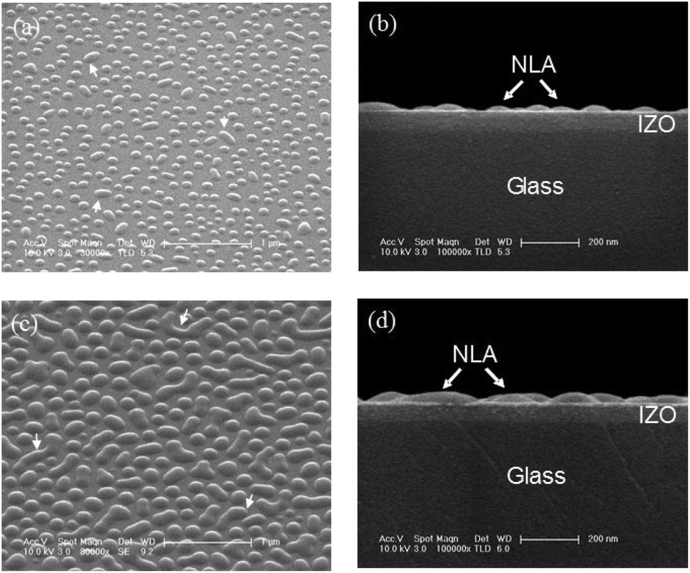 | ||
| Fig. 1 Planar (a, c) and cross sectional (b, d) SEM images of NLA 1 (a, b) and NLA 2 (c, d), showing the creation of the nano-lenses on the IZO layer by using the OVPD process. The arrows (a, c) indicate the impingement of the nano-lenses. | ||
By controlling the fabrication process, including the vaporizer pressure, nano-lenses with a diameter of 200–700 nm (NLA pattern 2) could be fabricated as presented in Fig. 1c and d, indicating that the diameter is controllable by controlling the process parameters. The coverage ratio of nano-lenses to the total surface is ∼70%. These morphologies indicate that islands nucleate in isolated areas and grow larger, impinging other islands.56
The nano-lenses in NLA 2 (which have a larger lens size) have a greater tendency to coalesce compared to the nano-lenses in NLA 1 (which have a smaller lens size). The results in Fig. 1 demonstrate that a size controllable NLA technology is developed using OVPD alone. Size control is an important technique because any kind of light can be chosen by adjusting the nano-lens diameter.
Crystallization and the resulting increase in surface tension
To study the difference in the growth characteristics of NPB films using the OVPD and the thermal evaporation processes, the crystallographic properties of the organic molecules were analyzed using GI-SAXS experiments. Three samples were prepared: a glass/IZO (60 nm) sample (Sample IZO), a glass/IZO (60 nm)/NPB planar film sample (60 nm, thermal evaporation) (Sample IZO/PL), and a glass/IZO (60 nm)/NLA 2 sample (Sample IZO/NLA). Sample IZO was used to identify the peaks of NPB among those of NPB, IZO, and glass.Fig. 2a explains the basic scheme of the GI-SAXS experiments, in which a synchrotron X-ray beam impinges on the specimen with a constant angle of incidence (αi), and the beam is scattered at an out-of-plane angle (αf) and an in-plane angle (2θf).57,58Fig. 2b–d are the GI-SAXS images of the three samples. The red color indicates a high scattering intensity. Fig. 2e and f present the q scan curves of the three specimens. The qxy and qz scan was carried out by cutting a line through the in-plane (qxy), and out-of-plane (qz) direction, respectively, at 2θf = 0°. Sample IZO/PL, deposited by thermal evaporation, has very broad NPB diffraction patterns (Fig. 2c) and q scan peaks (Fig. 2e), suggesting that the NPB molecules are stacked irregularly as an amorphous phase (Fig. 2g). In contrast, in the case of Sample IZO/NLA, the NPB diffraction peaks have sharp hemi-circles around the origin (Fig. 2d) and the q scan peaks are sharp (Fig. 2e and f), suggesting that the NLAs are composed of randomly oriented polycrystalline phases with small NPB crystallites. Thus, the NPB vapors crystallize to form the NLA in the OVPD process, but do not crystallize in the thermal evaporation process, instead forming a planar film.
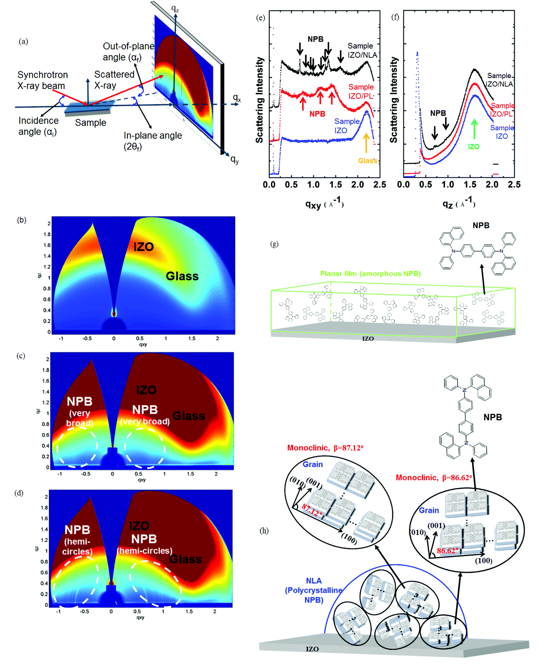 | ||
| Fig. 2 (a) The set-up of the GI-SAXS experiments, and the GI-SAXS images from (b) Sample IZO, (c) Sample IZO/PL, and (d) Sample IZO/NLA. (e) qxy and (f) qz scan results of (b), (c), and (d). The NPB stacking characteristics of (g) Sample IZO/PL, and (h) Sample IZO/NLA. | ||
To further examine the crystalline characteristics of the NPB crystallites in the NLA, the q scan peaks were indexed. The indexing was completed by assuming that there were two different crystals with monoclinic Bravais lattices, and that the organic molecules were positioned at the centers of the monoclinic lattices. The monoclinic system with a β value of 86.62° coincides with qxy values excluding 0.985 and 1.267, and the system with a β value of 87.12° coincides with those excluding 0.836, where β is an angle between the <100> and <001> axes (Table 1). Thus, the stacking is identified as the co-existence of the two monoclinic structure units (Fig. 2h).
| q xy [Å−1] | Monoclinic (β = 86.62°) | Monoclinic (β = 87.12°) |
|---|---|---|
| 0.695 | (010) | (010) |
| 0.836 | (101) | — |
| 0.940 | (100) | (100) |
| 0.985 | — | (101) |
| 1.160 | (110) | (110) |
| 1.267 | — | (111) |
| 1.385 | (020) | (020) |
| 1.600 | (001) | (001) |
The difference in morphology between the films grown by thermal evaporation and OVPD can be explained by the higher surface tension of the crystalline NPB layer compared to the amorphous layer, as explained in Fig. 3. If the surface tension of the substrate (γs) is larger than the sum of those of the thin film and the interface of the substrate-thin film (γt + γst), the thin film grows with a planar morphology (Fig. 3a). If γs is smaller than γt + γst, the thin film grows with an island morphology (Fig. 3b).59,60
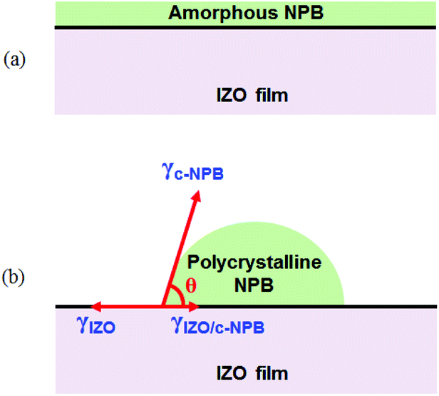 | ||
| Fig. 3 Schematic diagrams to explain the growth mode of (a) the amorphous NPB thin film on IZO with γIZO > γa-NPB + γIZO/a-NPB (Sample IZO/PL), and (b) an island consisting of polycrystalline NPB on IZO with γIZO < γc-NPB + γIZO/c-NPB (Sample IZO/NLA). Longer arrows indicate higher surface tension. θ is the contact angle. | ||
The even surface of the NPB layer grown by thermal evaporation on the IZO layer indicates that the sum of γa-NPB and γIZO/a-NPB is smaller than γIZO, where γa-NPB, γIZO/a-NPB, and γIZO are the surface tensions of the amorphous NPB, the interface between the IZO and amorphous NPB, and the IZO, respectively. In fact, the surface tension of the amorphous NPB (γa-NPB, 56.4 dyne per cm (ref. 61)) is reported to be smaller than that of the IZO film (γIZO, 90 dyne per cm (ref. 62)).
In contrast, the island growth of crystalline NBP on IZO by OVPD indicates that the sum of γc-NPB and γIZO/c-NPB is larger than γIZO, where γc-NPB, and γIZO/c-NPB are the surface tensions of the polycrystalline NPB, and the interface between IZO and polycrystalline NPB, respectively. In other words, γc-NPB is supposed to be higher than γa-NPB. This interpretation is supported by the variation in the surface tension depending on the crystallinity of the polymers due to a difference in density as reported before.63 For instance, crystalline polyethylene has a much higher surface tension (66.8 dyne per cm) than amorphous polyethylene (35.7 dyne per cm).63 Thus, the formation mechanism of the NLA can be established as crystallization of the NPB molecules and the resulting increase in surface tension.
Towards highly efficient and color stable OLEDs
To demonstrate the possible applications of size controllable NLAs, the light extraction layer of OLEDs is chosen as an example system. The effect of the NLA diameter on the light extraction efficiency was analyzed using optical simulations based on the FDTD method.30,64–66 A simple OLED structure consisting of Al (70 nm)/organic layer (150 nm)/IZO (50 nm) was used for the simulations. Dipole orientation was considered using a weighted linear combination of horizontal and vertical dipole light sources. Refractive indices of 0.85 and 2.0 were used for Al and IZO, corresponding to their values at a wavelength of 510 nm. The refractive indices of the organic layers and the NLA were assumed to be 1.8 with negligible extinction coefficients. The light extraction efficiency was determined as the ratio of the power flowing out of the device to the total power generated from the dipoles.The simulation results are summarized in Table 2. Use of NLA 1 and NLA 2 increased the light output efficiency by a factor of 1.02 and 1.48, respectively. The ∼1.5-fold change in the NLA 2 based device is believed to be due to the reduction of the guided modes by scattering at the NLA pattern, which also leads to a decrease in the absorption loss at the interface between the metal and organic layers. However, the light output ratio in the NLA 1 simulation is scarcely changed, which is believed to be due to the small size of the NLA which does not scatter the light efficiently.
| Structure | Extracted | Wave-guided | Absorption by metal | |
|---|---|---|---|---|
| fraction | Enhancement ratio | fraction | fraction | |
| w/o NLA | 0.304 | — | 0.271 | 0.425 |
| w/ NLA1 | 0.311 | 1.02 | 0.261 | 0.428 |
| w/ NLA2 | 0.451 | 1.48 | 0.183 | 0.366 |
The NLA containing nano-lenses with a diameter of several hundred nanometers (NLA 2) was easily integrated in the OLEDs by directly forming the NLA on the IZO top electrode (Fig. 4a). Fig. 4b presents the current density–voltage–luminous (J–V–L) plots of the devices without and with the NLAs. The J–V curves of the elements are similar and the turn-on voltages are the same (2.4 V), indicating that the OVPD process does not damage the device. The element with the NLA clearly shows a higher luminance than the element without the NLA. Fig. 4c displays that the current efficiency of OLEDs without and with the NLAs at 0.1 mA cm−2 is 79 and 123 cd A−1, respectively, showing an increased ratio of 1.55 by employing the NLA. The increased ratio is similar to that in the simulation results, indicating that the NLA is an optically effective scattering medium for OLEDs. Compared to the element without an NLA, the element with an NLA shows less photo image blurring and higher slope variation with the distance from the OLED center (Fig. 4d), indicating that the NLA provides less image blurring and increases color stability. Both devices without and with the NLAs show extremely small variation of color coordinates (Δu′v′: ∼0.002) as the viewing angle changes from 0° to 60°, which is due to the adoption of the IZO top electrode.67 The simulations using NLA 1 are also confirmed by the device data, which shows a 1.03 times increase in the current efficiency by NLA 1 integration.
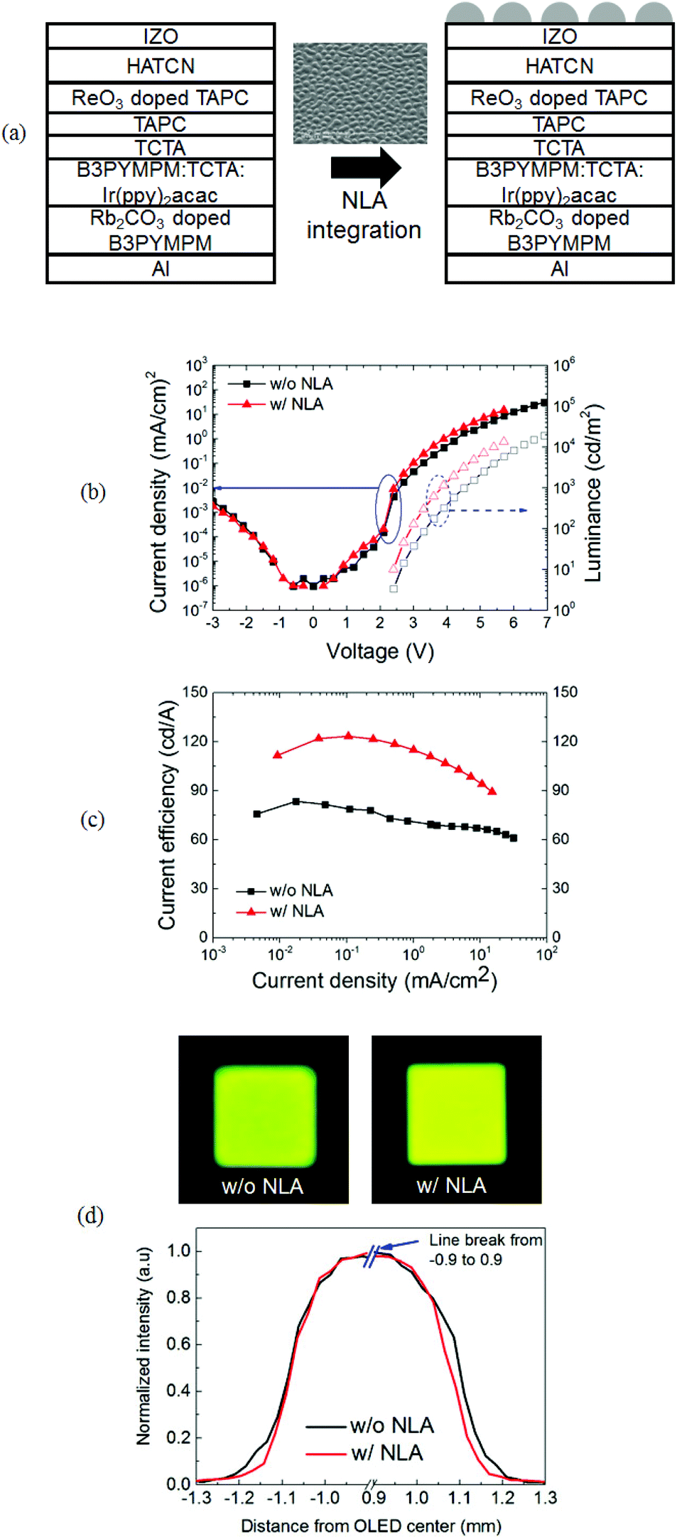 | ||
| Fig. 4 (a) Schematic diagrams of the inverted TOLEDs before and after the NLA integration. (b) The J–V–L curves, (c) the current efficiencies of the devices, showing a ∼1.5 times enhancement of efficiency after integration, and (d) less image blurring after integration. | ||
Conclusions
In conclusion, this work reports the development of a diameter controllable NLA technology using a conventional deposition (OVPD) technique. The formation mechanism of the NLA is interpreted and it is found that the NLA formation is reproducible in experiments in which the crystallization of organic molecules occurs.Targeting the light extraction layer of OLEDs, an NLA possessing nano-lenses with a diameter of several hundred nanometers was fabricated by controlling the process parameters. The presented NLA solves the issues of the non-compatibility and image blurring. The NLA increases the light extraction efficiency by a factor of ∼1.5, agreeing well with simulation results. Thus, the NLA is an optically effective scattering medium for OLEDs. Therefore, this NLA technology opens up the potential for low cost mass production of highly efficient and color stable OLEDs.
Acknowledgements
Y.-S. P., D.-H. C. and J. L. fabricated the NLA. K.-H. H. and Y. H. conducted the optical simulations. They fabricated and characterized the OLEDs without and with the NLAs. J. K., J. T. L. and Y.-S. P. performed the GI-SAXS analysis. Y.-S. P., K.-H. H., D.-H. C., N. S. C., B. Y., J.-K. L. and J.-J. K. analyzed all of the data and prepared the manuscript. The authors greatly appreciate the use of OVPD equipment from Dr S. Ahn (ETRI). This work was supported by a Korea Evaluation Institute of Industrial Technology (KEIT) grant funded by the Korea government (MOTIE) (Grant No. 10041062, Development of fundamental technology for light extraction of OLED).Notes and references
- K. Saxena, V. K. Jain and D. S. Meht, Opt. Mater., 2009, 32, 221 CrossRef CAS.
- H.-Y. Lin, Y.-H. Ho, J.-H. Lee, K.-Y. Chen, J.-H. Fang, S.-C. Hsu, M.-K. Wei, H.-Y. Lin, J.-H. Tsai and T.-C. Wu, Opt. Express, 2008, 16, 11044 CrossRef CAS PubMed.
- S. Möller and S. R. Forrest, J. Appl. Phys., 2002, 91, 3324 CrossRef.
- J.-B. Kim, J.-H. Lee, C.-K. Moon, K.-H. Kim and J.-J. Kim, Org. Electron., 2015, 17, 115 CrossRef CAS.
- T. Tsutsui, M. Yahiro, H. Yokogawa, K. Kawano and M. Yokoyama, Adv. Mater., 2001, 13, 1149 CrossRef CAS.
- Y.-R. Do, Y.-C. Kim, Y.-W. Song, C.-O. Cho, H.-S. Jeon, Y.-J. Lee, S.-H. Kim and Y.-H. Lee, Adv. Mater., 2003, 15, 1214 CrossRef CAS.
- H. Riel, S. Karg, T. Beierlein, W. Rieß and K. Neyts, J. Appl. Phys., 2003, 94, 5290 CrossRef CAS.
- C.-C. Wu, C.-L. Lin, P.-Y. Hsieh and H.-H. Chiang, Appl. Phys. Lett., 2004, 84, 3966 CrossRef CAS.
- Y.-H. Cheng, J.-L. Wu, C.-H. Cheng, K.-C. Syao and M.-C. M. Lee, Appl. Phys. Lett., 2007, 90, 091102 CrossRef.
- C.-J. Yang, S.-H. Liu, H.-H. Hsieh, C.-C. Liu, T.-Y. Cho and C.-C. Wu, Appl. Phys. Lett., 2007, 91, 253508 CrossRef.
- S. Reineke, F. Lindner, G. Schwartz, N. Seidler, K. Walzer, B. Lüssem and K. Leo, Nature, 2009, 459, 234 CrossRef CAS PubMed.
- C.-C. Liu, S.-H. Liu, K.-C. Tien, M.-H. Hsu, H.-W. Chang, C.-K. Chang, C.-J. Yang and C.-C. Wu, Appl. Phys. Lett., 2009, 94, 103302 CrossRef.
- A. O. Altun, S.-H. Jeon, J.-Y. Shim, J.-H. Jeong, D.-G. Choi, K.-D. Kim, J.-H. Choi, S.-W. Lee, E.-S. Lee, H.-D. Park, J. R. Youn, J.-J. Kim, Y.-H. Lee and J.-W. Kang, Org. Electron., 2010, 11, 711 CrossRef CAS.
- W. H. Koo, S. M. Jeong, F. Araoka, K. Ishikawa, S. Nishimura, T. Toyooka and H. Takezoe, Nat. Photonics, 2010, 4, 222 CrossRef CAS.
- M. Thomschke, S. Reineke, B. Lüssem and K. Leo, Nano Lett., 2012, 12, 424 CrossRef CAS PubMed.
- K. Hong, H. K. Yu, I. Lee, K. Kim, S. Kim and J.-L. Lee, Adv. Mater., 2010, 22, 4890 CrossRef CAS PubMed.
- Y. Jin, J. Feng, X.-L. Zhang, Y.-G. Bi, Y. Bai, L. Chen, T. Lan, Y.-F. Liu, Q.-D. Chen and H.-B. Sun, Adv. Mater., 2012, 24, 1187 CrossRef CAS PubMed.
- E. Wrzesniewski, S.-H. Eom, W. Cao, W. T. Hammond, S. Lee, E. P. Douglas and J. Xue, Small, 2012, 8, 2647 CrossRef CAS PubMed.
- J.-B. Kim, J.-H. Lee, C.-K. Moon, S.-Y. Kim and J.-J. Kim, Adv. Mater., 2013, 25, 3571 CrossRef CAS PubMed.
- C. Lee and J.-J. Kim, Small, 2013, 9, 3858 CrossRef CAS PubMed.
- J.-W. Shin, D.-H. Cho, J. Moon, C. W. Joo, S. K. Park, J. Lee, J.-H. Han, N. S. Cho, J. Hwang, J. W. Huh, H. Y. Chu and J.-I. Lee, Org. Electron., 2014, 15, 196 CrossRef CAS.
- L. Zhou, Q.-D. Ou, J.-D. Chen, S. Shen, J.-X. Tang, Y.-Q. Li and S.-T. Lee, Sci. Rep., 2014, 4, 4040 CrossRef PubMed.
- T. Schwab, C. Fuchs, R. Scholz, A. Zakhidov, K. Leo and M. C. Gather, Opt. Express, 2014, 22, 7524 CrossRef CAS PubMed.
- Y.-G. Bi, J. Feng, Y.-S. Liu, Y.-F. Li, Y. Chen, X.-L. Zhang, X.-C. Han and H.-B. Sun, Sci. Rep., 2014, 4, 7108 CrossRef CAS PubMed.
- S. Jeon, J.-H. Lee, J.-H. Jeong, Y. S. Song, C.-K. Moon, J.-J. Kim and J. R. Youn, Sci. Rep., 2015, 5, 8685 CrossRef CAS PubMed.
- E. Kim, H. Cho, K. Kim, T.-W. Koh, J. Chung, J. Lee, Y. Park and S. Yoo, Adv. Mater., 2015, 27, 1624 CrossRef CAS PubMed.
- Y. Qu, M. Slootsky and S. R. Forrest, Nat. Photonics, 2015, 9, 758 CrossRef CAS.
- C.-Y. Chen, W.-K. Lee, Y.-J. Chen, C.-Y. Lu, H. Y. Lin and C.-C. Wu, Adv. Mater., 2015, 27, 4883 CrossRef CAS PubMed.
- C. Lee, K.-H. Han, K.-H. Kim and J.-J. Kim, Opt. Express, 2016, 24, A488 CrossRef CAS PubMed.
- B. Pyo, C. W. Joo, H. S. Kim, B.-H. Kwon, J.-I. Lee, J. Lee and M. C. Suh, Nanoscale, 2016, 8, 8575 RSC.
- J. Lee, W. J. Sung, C. W. Joo, H. Cho, N. S. Cho, G.-W. Lee, D.-H. Hwang and J.-I. Lee, ETRI J., 2016, 38, 260 CrossRef.
- C. W. Joo, J. Moon, J.-H. Han, J. W. Huh, J.-W. Shin, D.-H. Cho, J. Lee, N. S. Cho and J.-I. Lee, J. Inf. Disp., 2015, 16, 161 CrossRef CAS.
- K. Lee, J.-W. Shin, J.-H. Park, J. Lee, C. W. Joo, J.-I. Lee, D.-H. Cho, J. T. Lim, M.-C. Oh, B.-K. Ju and J. Moon, ACS Appl. Mater. Interfaces, 2016, 8, 17409 Search PubMed.
- J. W. Huh, J.-W. Shin, D.-H. Cho, J. Moon, C. W. Joo, S. K. Park, J. Hwang, N. S. Cho, J. Lee, J.-H. Han, H. Y. Chu and J.-I. Lee, Nanoscale, 2014, 6, 10727 RSC.
- J. H. Hwang, H. J. Lee, Y. S. Shim, C. H. Park, S.-G. Jung, K. N. Kim, Y. W. Park and B.-K. Ju, Nanoscale, 2015, 7, 2723 RSC.
- Y. S. Shim, J. H. Hwang, C. H. Park, S.-G. Jung, Y. W. Park and B.-K. Ju, Nanoscale, 2016, 8, 4113 RSC.
- D.-H. Cho, J.-W. Shin, J. Moon, S. K. Park, C. W. Joo, N. S. Cho, J. W. Huh, J.-H. Han, J. Lee, H. Y. Chu and J.-I. Lee, ETRI J., 2014, 36, 847 CrossRef.
- J.-W. Shin, D.-H. Cho, J. Moon, C. W. Joo, J. Lee, J. W. Huh, S. K. Park, J.-H. Han, N. S. Cho, J. Hwang, H. Y. Chu and J.-I. Lee, Opt. Lett., 2014, 39, 3527 CrossRef CAS PubMed.
- J. Moon, E. Kim, S. K. Park, K. Lee, J.-W. Shin, D.-H. Cho, J. Lee, C. W. Joo, N. S. Cho, J.-H. Han, B.-G. Yu, S. Yoo and J.-I. Lee, Org. Electron., 2015, 26, 273 CrossRef CAS.
- W. H. Koo, Y. Zhe and F. So, Adv. Opt. Mater., 2013, 1, 404 CrossRef.
- W. H. Koo, W. Youn, P. Zhu, X.-H. Li, N. Tansu and F. So, Adv. Funct. Mater., 2012, 22, 3454 CrossRef CAS.
- L.-H. Xu, Q.-D. Ou, Y.-Q. Li, Y.-B. Zhang, X.-D. Zhao, H.-Y. Xiang, J.-D. Chen, L. Zhou, S.-T. Lee and J.-X. Tang, ACS Nano, 2016, 10, 1625 CrossRef CAS PubMed.
- H. Kaji, H. Suzuki, T. Fukushima, K. Shizu, K. Suzuki, S. Kubo, T. Komino, H. Oiwa, F. Suzuki, A. Wakamiya, Y. Murata and C. Adachi, Nat. Commun., 2015, 6, 8476 CrossRef CAS PubMed.
- H. Fujimoto, M. Yahiro, T. Kawashima, K. Konno, Q. Chen, K. Sawaya, S. Kawakami and C. Adachi, Appl. Phys. Express, 2015, 8, 082102 CrossRef.
- J.-H. Jou, W.-B. Wang, M.-F. Hsu, J.-J. Shyue, C.-H. Chiu, I.-M. Lai, S.-Z. Chen, P.-H. Wu, C.-C. Chen, C.-P. Liu and S.-M. Shen, ACS Nano, 2010, 4, 4054 CrossRef CAS PubMed.
- H. Lee, J. Kwak, C.-M. Kang, Y.-Y. Lyu, K. Char and C. Lee, Opt. Express, 2015, 23, 11424 CrossRef CAS PubMed.
- W. Wang, H. Peng, S. Wang and S. Chen, Org. Electron., 2015, 24, 195 CrossRef CAS.
- S. Chen and H.-S. Kwok, Isr. J. Chem., 2014, 54, 847 CrossRef CAS.
- S. Chen, W. Qin, Z. Zhao, B. Z. Tang and H.-S. Kwok, J. Mater. Chem., 2012, 22, 13386 RSC.
- S. Chen, Z. Zhao, B. Z. Tang and H.-S. Kwok, Org. Electron., 2012, 13, 1996 CrossRef CAS.
- C.-C. Ma, Y.-J. Chen and L.-J. Hsiao, Proc. SPIE 9137 Organic Photonics VI, 2014, p. 91370J.
- http://www.lumerical.com/tcad-products/fdtd .
- P. E. Burrows, S. R. Forrest, L. S. Sapochak, J. Schwartz, P. Fenter, T. Buma, V. S. Ban and J. L. Forrest, J. Cryst. Growth, 1995, 156, 91 CrossRef CAS.
- M. Baldo, M. Deutsch, P. Burrows, H. Gossenberger, M. Gerstenberg, V. Ban and S. Forrest, Adv. Mater., 1998, 10, 1505 CrossRef CAS.
- M. A. Baldo, V. G. Kozlov, P. E. Burrows, S. R. Forrest, V. S. Ban, B. Koene and M. E. Thompson, Appl. Phys. Lett., 1997, 71, 3033 CrossRef CAS.
- S. C. Seel and C. V. Thompson, J. Appl. Phys., 2003, 93, 9038 CrossRef CAS.
- J. Rivnay, S. C. B. Mannsfeld, C. E. Miller, A. Salleo and M. F. Toney, Chem. Rev., 2012, 112, 5488 CrossRef CAS PubMed.
- J. Perlich, G. Kaune, M. Memesa, J. S. Gutmann and P. Müller-Buschbaum, Philos. Trans. R. Soc. London, Ser. A, 2009, 367, 1783 CrossRef CAS PubMed.
- P. G. de Gennes, Rev. Mod. Phys., 1985, 57, 827 CrossRef CAS.
- D. J. Eaglesham and M. Cerullo, Phys. Rev. Lett., 1990, 64, 1943 CrossRef CAS PubMed.
- http://www.lookchem.com/N-N-Bis-1-naphthalenyl-N-N-bisphenyl-1-1-biphenyl-4-4-diamine/ .
- Y.-S. Park, K.-H. Choi and H.-K. Kim, Electrochem. Solid-State Lett., 2009, 12, H426 CrossRef CAS.
- S. Wu, in Polymer Interface and Adhesion, Marcel Dekker Inc., New York, NY, USA, 1982, Morphological effect on surface tension, 201 Search PubMed.
- A. Chutinan, K. Ishihara, T. Asano, M. Fujita and S. Noda, Org. Electron., 2005, 6, 3 CrossRef CAS.
- J.-W. Kim, J.-H. Jang, M.-C. Oh, J.-W. Shin, D.-H. Cho, J. Moon and J.-I. Lee, Opt. Express, 2014, 22, 498 CrossRef PubMed.
- S. Jeon, J.-H. Jeong, Y. S. Song, W.-I. Jeong, J.-J. Kim and J. R. Youn, Nanoscale, 2014, 6, 2642 RSC.
- J.-B. Kim, J.-H. Lee, C.-K. Moon and J.-J. Kim, Appl. Phys. Lett., 2014, 104, 073301 CrossRef.
Footnotes |
| † Electronic supplementary information (ESI) available: Additional information about refractive indices and extinction coefficients of the Al and IZO utilized for the optical simulations. See DOI: 10.1039/c6nr07798f |
| ‡ Co-first authors. |
| This journal is © The Royal Society of Chemistry 2017 |