
Electrosprayed TiO2 nanoporous hemispheres for enhanced electron transport and device performance of formamidinium based perovskite solar cells†
Tao
Ye‡
ab,
Shaoyang
Ma‡
c,
Xi
Jiang
d,
Miloš
Petrović
ab,
Chellappan
Vijila
 *b,
Seeram
Ramakrishna
*ab and
Lei
Wei
*c
*b,
Seeram
Ramakrishna
*ab and
Lei
Wei
*c
aDepartment of Mechanical Engineering, National University of Singapore, Singapore 117576, Singapore. E-mail: seeram@nus.edu.sg
bInstitute of Materials Research and Engineering (IMRE), Agency for Science, Technology and Research (A*STAR), #08-03, 2 Fusionopolis Way, Innovis, 138634, Singapore. E-mail: c-vijila@imre.a-star.edu.sg
cSchool of Electrical and Electronic Engineering, Nanyang Technological University, Singapore 639798, Singapore. E-mail: wei.lei@ntu.edu.sg
dDepartment of Chemical and Biomolecular Engineering, National University of Singapore, Singapore 117585, Singapore
First published on 30th November 2016
Abstract
Titanium dioxide (TiO2) nanoporous hemispheres (NHSs) with a radius of ∼200 nm are fabricated by electrospraying a hydrothermally synthesized TiO2 nanoparticle (NP) suspension solution. The resulting TiO2 NHSs are highly porous, which are beneficial to the infiltration of perovskites and provide a larger contact area, as building blocks to construct a mesoporous TiO2 layer for FA0.81MA0.15Pb(I0.836Br0.15)3 based perovskite solar cells (PSCs). By varying the TiO2 NHS collecting period (15 s, 30 s, 60 s and 90 s) during the electrospraying process, the performance of PSCs changes with different TiO2 NHS distribution densities. The optimized PSC employing TiO2 NHSs (60 s) exhibits a photovoltaic conversion efficiency (PCE) as high as 19.3% with a Jsc of 23.8 mA cm−2, a Voc of 1.14 V and a FF of 0.71. Furthermore, the PSC possesses a reproducible PCE value with little hysteresis in its current density–voltage (J–V) curves. The small perturbation transient photovoltage (TPV) measurement reveals a longer free carrier lifetime within the TiO2 NHS based PSC than that in the TiO2 NP based PSC, and the time of flight (TOF) photoconductivity measurement shows that charge mobilities in this system are also enhanced. These characteristics make TiO2 NHSs a promising electron transport material for efficient photovoltaic devices.
Introduction
Metal halide perovskites with the formula APbB3 [A = Cs+, MA (CH3NH3+, methylammonium cation) or FA (NH = CHNH3+, formamidinium cation); B = Cl−, Br− and I−], as emerging light absorbing materials, offer a promising path to construct highly efficient photovoltaic devices, owing to their unique optoelectronic properties, including large optical tunability, high absorption coefficients and millimeter-scale carrier diffusion length. The efficiency of perovskite solar cells (PSCs) has kept growing in recent years and the highest efficiency reported is 22.1% up to now.1–11 Among the recently proposed PSC architectures, the mesoporous TiO2 layer functions as an “active” scaffold to enable electron transportation from the perovskite light-absorber to the fluorine doped tin oxide (FTO) layer through its conduction band (CB).2–13 Therefore, the mesoporous TiO2 layer is required to be: (1) unconsolidated to accept the perovskite, (2) nanoporous to enlarge the contact area with the perovskite to obtain highly efficient charge injection, and (3) defect-free to minimize grain boundaries for the purpose of suppressing charge recombination and trapping.13 As the thickness of the TiO2 layer strongly affects the efficiency of mesoscopic PSCs, a submicron thick (200–300 nm) mesoporous TiO2 layer made from TiO2 nanoparticles (NPs) with a size of 20–50 nm is commonly adopted to enhance the electron transportation and minimize the loss of electrons caused by the charge recombination when fabricating PSCs.14–19 While tiny TiO2 NPs with a large surface area possess small pores that will block the effective infiltration of the perovskite, large TiO2 NPs with a better infiltration ability of the perovskite normally generate a small surface area.13 For this reason, nanoporous TiO2 spherical structures (SPs) synthesized by different methods,20–37 which have been applied in dye sensitized solar cells20,21,26–31 and quantum dot solar cells,32–36 are introduced to replace TiO2 NPs in PSCs13,37 and reveal superiorities over TiO2 NPs in both providing a large surface area for the deposition of perovskites and generating efficient porous structures for electrolyte diffusion. For example, a notable photovoltaic conversion efficiency (PCE) improvement has been achieved from 14.73% of a 30 nm TiO2 NP based PSC to 18.41% of a 100 nm TiO2 SP based device.13 However, the large TiO2 SP diameter significantly reduces the contact area between nanoporous TiO2 SPs and the substrate, which further holds back the electron injection from the TiO2 SP CB into the substrate. To solve this, mechanical compression treatment, which can increase the inter-particles connection as well as the contact area with the substrate, has been used in dye sensitized solar cells,20,21 but this will cause counteracting of the enlarged pores brought about by SPs and potential risk to mechanically damage the compact TiO2 layer or the FTO substrate.Here, we establish a fabrication method which yields TiO2 nanoporous hemispheres (NHSs) by electrospraying hydrothermally synthesized TiO2 NP suspension solution in a controllable and scalable manner. The “soft” touch of the electrosprayed TiO2 on the “hard” FTO/compact TiO2 substrate automatically forms hemispherical structures. The resulting TiO2 NHSs are monodispersed with ultralarge surface areas and a considerable number of pores to improve the infiltration of the perovskite, and the large surface area increases the contact area between the perovskite and TiO2 NHSs, leading to efficient electron injection. All these properties make them preferable to replace the conventional mesoporous TiO2 NP layer. Moreover, TiCl4 treatment is applied to provide strong interconnectivity among the TiO2 NPs within the TiO2 NHS, making the charge transportation through the TiO2 layer more efficient. We demonstrate that the fabricated TiO2 layer formed by electrosprayed TiO2 NHSs greatly enhances the photovoltaic properties of PSCs. Furthermore, we systematically study the origin of the enhanced photovoltaic properties of PSCs based on TiO2 NHSs by performing small perturbation transient photovoltage (TPV) and time of flight (TOF) photoconductivity measurements to analyze the free carriers lifetime and mobilities.
Experimental section
Synthesis of MABr
MABr was synthesized by slowly dropping hydrobromic acid (48 wt% in water, Sigma-Aldrich) into a solution of CH3NH2 (33 wt% solution in absolute ethanol, Sigma-Aldrich) at 0 °C.11 The solution was magnetically stirred for 4 hours at room temperature, followed by rotary evaporation at 50 °C until no obvious liquid remained. The crude solid was then dissolved in a small amount of ethanol (Sigma-Aldrich), and reprecipitated with diethyl ether (Sigma-Aldrich) three times. The resulting white solid was collected and dried at room temperature under vacuum for 2 days before usage.Synthesis of TiO2 nanoparticles
Titanium isopropoxide (Sigma-Aldrich) was used as a TiO2 precursor. Acetic acid (Sigma-Aldrich) and nitric acid (Sigma-Aldrich) were used to control the pH (around 1 with roughly 0.1 M H+) of the solution, and the solution was transferred to Teflon cups in an autoclave for the following hydrothermal process (240 °C for 15 hours).38 TiO2 paste was prepared by adding 0.65 g TiO2 nanoparticles and 0.5 g ethyl cellulose (Sigma-Aldrich) into 3.22 mL α-terpineol (Sigma-Aldrich) and 3.22 mL methoxyethanol (Sigma-Aldrich). The paste was then sonicated for 2 hours until a homogeneous suspension solution without aggregation was obtained. Next, the TiO2 paste was diluted with ethanol in a weight ratio of 1![[thin space (1/6-em)]](https://www.rsc.org/images/entities/char_2009.gif) :10. The diluted solution was loaded into a plastic syringe which was connected to a high voltage power supply, and then electrosprayed directly onto the compact TiO2 layer.
:10. The diluted solution was loaded into a plastic syringe which was connected to a high voltage power supply, and then electrosprayed directly onto the compact TiO2 layer.
Fabrication of PSCs
The patterned FTO-coated glass (NSG) was sequentially cleaned using detergent, DI water, acetone (Sigma-Aldrich), and isopropanol (Sigma-Aldrich) and finally treated under UV ozone for 10 minutes at 100 °C. A thin compact TiO2 (C-TiO2) layer was deposited on top of the cleaned FTO substrate by spin-coating the TiO2 flat film precursor solution at 6000 rpm for 30 s and dried at 120 °C for 5 minutes in a nitrogen (N2) glovebox. Then, it was gradually heated up to 450 °C for 30 minutes in air. To prepare the TiO2 flat film precursor solution, titanium isopropoxide (1 mL, Sigma-Aldrich) and 12 M HCl solution (10 μL, Sigma-Aldrich) were diluted in ethanol (10 mL). Then the substrate was treated with a 50 mM TiCl4 (Sigma-Aldrich) aqueous solution at 80 °C for 20 minutes followed by annealing at 450 °C for 20 minutes. To prepare the TiO2 NHSs with a radius of about 200 nm, the electrospraying process was carried out with a commercial electrospinning setup (ET-2535, Ucalery). The electric field of 15 kV was applied between the metal orifice and the conducting collector, and the solution feeding rate was controlled by using a syringe pump at 0.3 mL h−1. The electrospraying process generates droplets and simultaneously applies a charge by means of an electric field. During the electrospraying process, particle stacking proceeds under the forces of the electric field and liquid surface tension. The final shape of the TiO2 NHSs was controlled by adjusting the parameters of the electrospraying process, including voltage (15 kV), collecting distance (10 cm), humidity (50%–70%) and feeding rate (0.3 mL h−1), to ensure when the droplets reached the collector, the solvent was not evaporated completely. The shape of TiO2 NHSs is therefore deformable, which further leads to a flat contact area with the substrate. The collecting periods are 15 s, 30 s, 60 s and 90 s, respectively. After the electrospraying process, the as-prepared TiO2 meso-layer was placed on a hot plate and sintered at 500 °C for 20 minutes in air. Then, the substrate was treated with a 50 mM TiCl4 (Sigma-Aldrich) aqueous solution at 80 °C for 20 minutes followed by annealing at 500 °C for 15 minutes. For the fabrication of the TiO2 NP PSC, an ∼180 nm thick TiO2 NP layer was deposited on top of the substrate by spin-coating the prepared TiO2 paste (the other procedures are the same as the TiO2 NHS PSC). Next, the perovskite film was deposited on the substrate by a spin-coating process in a glovebox: first, 2000 rpm for 10 s; second, 6000 rpm for 30 s, and then chlorobenzene (110 mL, Sigma-Aldrich) was dropped in 8–10 s during the second spin-coating process. The substrate was then heated at 100 °C for 60 minutes. The recipe of the precursor solution was the same as a recent study:11 the precursor solution was prepared by dissolving 0.265 g PbI2 (TCI), 0.037 g PbBr2 (TCI), 0.011 g MABr and 0.094 g FAI (Dyesol) in 0.4 mL anhydrous N,N-dimethylformamide (Sigma-Aldrich) and 0.1 mL anhydrous dimethylsulfoxide (Sigma-Aldrich). Spiro-OMeTAD (Merck) was further deposited by spin-coating at 3000 rpm for 30 s. The spiro-OMeTAD solution was prepared by dissolving 74 mg spiro-OMeTAD, 28.5 μL 4-tert-butylpyridine (Sigma-Aldrich), 17.5 μL of a stock solution of 520 mg mL−1 lithium bis (trifluoromethylsulphonyl) imide (Sigma-Aldrich) in acetonitrile (Sigma-Aldrich) and 29 μL of a stock solution of 100 mg mL−1 tris(2-(1H-pyrazol-1-yl)-4-tert-butylpyridine)-cobalt(III) tris(bis(trifluoromethylsulfonyl) imide) (Sigma-Aldrich) in acetonitrile in 1 mL anhydrous chlorobenzene. Finally, 80 nm of gold was deposited as an electrode by thermal evaporation at an average deposition rate of 0.3 Å s−1. Epoxy was used to protect the fabricated devices from coming into contact with moisture and the encapsulated devices were collected in a desiccator for the stability study.11Characterization
J–V characterization was performed in an inert environment (MBraun glovebox, N2 atmosphere) with a solar simulator (SAN-EI Electric XES-301S 300 W Xe lamp JIS Class AAA) and a Keithley 2400 sourcemeter. The solar cells were masked with metal apertures to define the active areas which were typically 0.09 or 0.08 cm2. The incident photon-to-current efficiency (IPCE) as a function of light wavelength was measured in the same glovebox with a customer-made setup consisting of an Oriel 300 W Xe lamp in combination with an Oriel Cornerstone 130 monochromator and a SRS 810 lock-in amplifier (Stanford Research Systems). A calibrated Si diode was used as the reference to calculate the number of photons incident on the device for each wavelength. The IPCE photocurrent was recorded by using a Keithley 2400 sourcemeter. The surface and cross section morphologies of perovskite films and the entire PSCs were investigated by using a scanning electron microscope (SEM, JEOL 6340F) at 5 kV. The morphologies of the prepared TiO2 NPs and NHSs were studied by using a transmission electron microscope (TEM, JEOL 2100F) at 200 kV. X-ray diffraction (XRD) experiments were conducted by using a Shimadzu XRD-6000 X-ray diffractometer with Cu Kα radiation (λ = 1.54 Å). The simulations of optical power distribution within the functional layers were conducted by means of finite-difference time-domain methods (Lumerical FDTD Solutions). The absorption spectra were recorded on a PerkinElmer Lambda 950UV/VIS/NIR spectrometer. TOF photoconductivity measurements were carried out by generating the photocarriers at the FTO side of the device, and a pulsed Nd:YAG laser (wavelength of 532 nm, pulse width <4 ns, and pulse repetition rate 1 Hz) was used as the light source for the TOF experiment. Small perturbation TPV experiments were performed using the same laser, and the power intensity of the laser was adjusted by using neutral density filters to afford a small perturbation of the cell photovoltage (∼20 mV). A white light halogen lamp and neutral density filters were employed to vary the back illumination level. The photocurrents under different applied electric fields were documented by using an oscilloscope (Agilent 54845A).Results and discussion
In order to study the photovoltaic properties of electrosprayed TiO2 NHS based PSCs, TiO2 NPs are first synthesized using a hydrothermal method, and then TiO2 NHSs are fabricated by electrospraying this TiO2 NP suspension solution. Fig. 1 schematically illustrates the fabrication process of both TiO2 NHS based PSC and its control group based on conventional TiO2 NPs.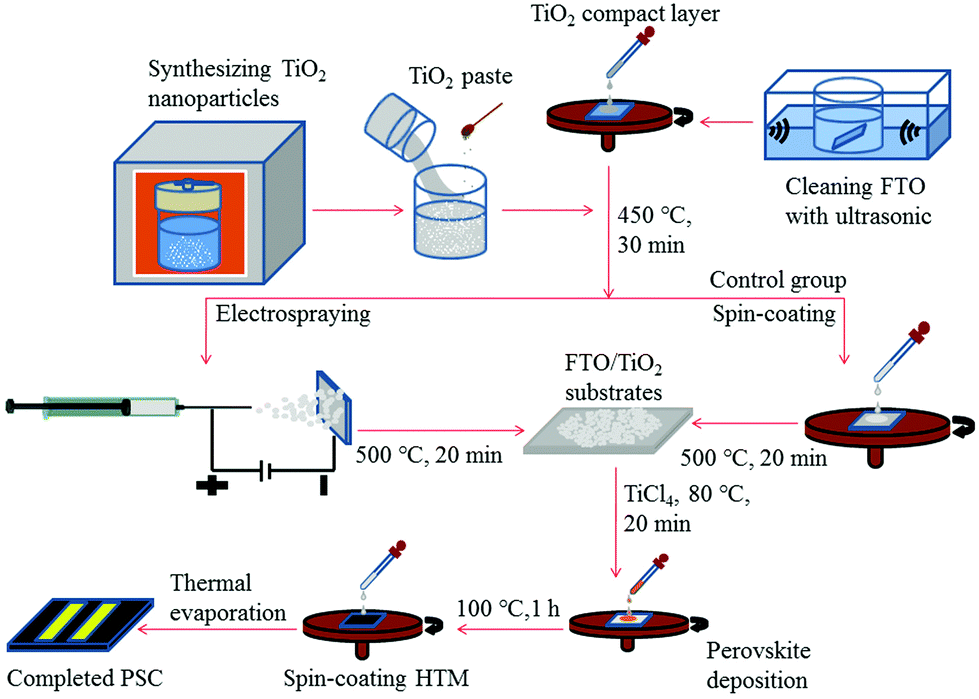 | ||
| Fig. 1 Fabrication process of PSCs. | ||
The TiO2 NPs are fabricated by a hydrothermal method with titanium isopropoxide as the precursor under acidic conditions (pH ∼ 1). The concentration of H+ in the solution is a critical factor to determine the synthesis product when preparing TiO2 by hydrothermal reaction. To be specific, when under extreme acidic conditions (pH < 0), rutile TiO2 is usually formed, while anatase TiO2 is obtainable under significantly less acidic conditions (pH > 1).12,38–40 So both acetic acid and nitric acid are used in our process to adjust the pH value of the aqueous solution. The SEM (Fig. 2a) and TEM images of different magnifications (Fig. 2b and c) present the mesoscopic and morphological structure of the synthesized TiO2 NPs. Fig. 2b shows a group of TiO2 NPs with an average size of 30 nm which is well controlled and uniformly distributed. High resolution TEM (Fig. 2c) illustrates the crystal structure of the synthesized TiO2 NPs, which is oriented along the [101] direction, similar to some previously reported results.39,40 To reveal the structure of the TiO2 NPs in this study, the XRD pattern (Fig. 2d) is recorded, and the well-resolved diffraction peaks are indexed to (101), (004), (200), (105), (211), (204) and (215), indicating the anatase nature of the synthesized TiO2 NPs.12,13,38–40
 | ||
| Fig. 2 (a) SEM; (b) low-magnification TEM; (c) high-resolution TEM images, and (d) XRD pattern of the hydrothermal synthesized TiO2 NPs. The SEM image (a) and XRD spectrum (d) were documented from a sample fabricated by spin-coating TiO2 NPs on top of the FTO/C-TiO2 substrate; to obtain the TEM images, the TiO2 NPs were deposited on the copper mesh TEM grids for the measurement. | ||
TiO2 NHSs are fabricated by electrospraying the suspension solution of TiO2 NPs and then form a dense structure due to the evaporation of the solvent. The SEM and TEM images of the electrosprayed TiO2 NHSs are shown in Fig. 3. Compared to TiO2 spherical structures formed with fully and ultrafast evaporation of the solvent during electrospraying,20,21 we control both the size and shape of TiO2 NHSs by adjusting various parameters during the electrospraying process. More precisely, by employing a relatively shorter collecting distance, a larger feeding rate and higher humidity, only a small amount of solvent remains within the suspension droplets when they reach the substrate. With the high momentum provided by the electric field, the droplets deform into hemispherical structures with flat surfaces contacting with the substrate. Fig. 3a and b clearly show the hemispherical structure of a single TiO2 NHS and a group of TiO2 NHSs on top of a FTO/compact TiO2 substrate. TiO2 NHSs are highly porous structures, as shown in Fig. 3c, which will improve the infiltration of the perovskite light-absorber into the mesoporous TiO2 layer. However, the interconnectivity among the TiO2 NPs within the electrosprayed TiO2 NHS is weak, which may suppress the electron transport within the TiO2 NHSs. So, we utilize diluted TiCl4 aqueous solution to treat the as-electrosprayed TiO2 NHSs for the purpose of improving the interconnectivity of the TiO2 NPs.20,21Fig. 3c and e show the TiO2 NHSs before the TiCl4 treatment, and Fig. 3d and f are the images of TiO2 NHSs after the treatment. TiO2 NPs within TiO2 NHSs after being treated with TiCl4 are connected more strongly than the case before the treatment, which provides a fast transporting channel for photogenerated electrons to transport inside the TiO2 NHSs.
 | ||
| Fig. 3 Side view SEM images of (a) a single TiO2 NHS and (b) a 60 s collecting time sample on the FTO/compact TiO2 substrate. Plan view SEM images of TiO2 NHSs (c) before and (d) after TiCl4 treatment; TEM images of TiO2 NHSs (e) before and (f) after TiCl4 treatment. | ||
The prepared TiO2 NHSs are then employed to fabricate the mesoporous TiO2 layer. For comparison, the same TiO2 NPs synthesized by hydrothermal reaction are also applied using a spin-coating method as a control group. Then the FA0.81MA0.15Pb(I0.836Br0.15)3 layer is deposited on the mesoporous TiO2 layers by a two-step spin-coating process.11Fig. 4a shows the surface morphology of the prepared FA0.81MA0.15Pb(I0.836Br0.15)3 layer. Compared to the control group (Fig. S1†), the crystal size of the FA0.81MA0.15Pb(I0.836Br0.15)3 film is more uniform on the electrosprayed TiO2 NHS layer than that on the TiO2 NP layer. In addition, the average ∼400 nm FA0.81MA0.15Pb(I0.836Br0.15)3 crystal size is observed (with the range of 300–600 nm) in the TiO2 NHS sample, while the average crystal size in the TiO2 NP sample is ∼250 nm with the range of 100–450 nm. The large average crystal size and even size distribution of the deposited FA0.81MA0.15Pb(I0.836Br0.15)3 on top of the TiO2 NHS layer lead to less grain boundaries within the perovskite film, which reduces the recombination and trapping probability in the injection and transportation processes of photogenerated free electrons.13 XRD spectra (Fig. S2†) show that the intensities and band widths of FA0.81MA0.15Pb(I0.836Br0.15)3 peaks are not varied due to the change of the mesoporous TiO2 layer, and the characteristic XRD peak positions of the prepared FA0.81MA0.15Pb(I0.836Br0.15)3 samples are identical to the previous results.11
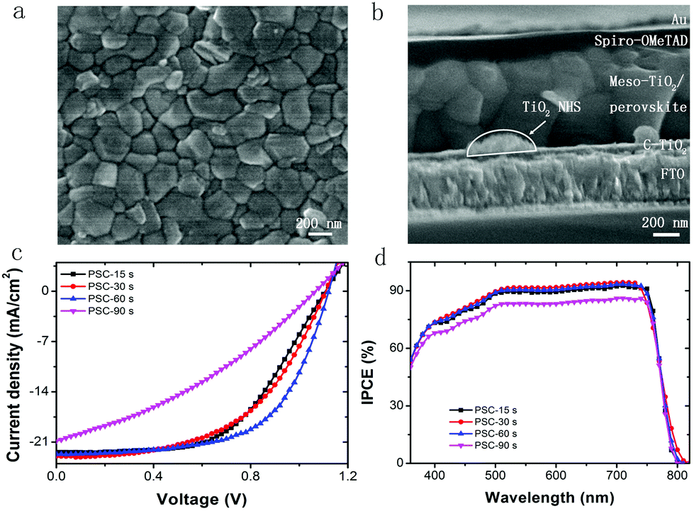 | ||
| Fig. 4 (a) Surface SEM image of the FA0.81MA0.15Pb(I0.836Br0.15)3 film based on TiO2 NHSs; (b) cross-section SEM image of TiO2 NHS based PSC. Photovoltaic performance: (c) J–V curves; and (d) IPCE of PSCs with different collecting time of TiO2 NHSs. | ||
Next, FA0.81MA0.15Pb(I0.836Br0.15)3 based PSCs are fabricated as described in Fig. 1. Fig. 4b shows the cross-sectional SEM image of the fabricated PSC employing electrosprayed TiO2 NHSs with the collecting period of 30 s, which gives the thickness and morphology for each functional layer of the device. As demonstrated, the functional layers within the PSC from bottom to top are FTO, a compact TiO2 layer (∼40 nm), a mesoporous TiO2 layer with FA0.81MA0.15Pb(I0.836Br0.15)3 (∼600 nm), HTM (∼150 nm) and a Au electrode (∼80 nm), respectively. Each layer connects tightly to its adjacent layers, which enables the unimpeded interlayer transport of photogenerated free carriers. As can be seen from the image, a few TiO2 NHSs located above the TiO2 compact layer and the FA0.81MA0.15Pb(I0.836Br0.15)3 film show high crystallinity.
PSCs with a different collecting period of TiO2 NHSs are fabricated. Fig. 4c presents the typical current density–voltage (J–V) curves for these resulting devices. Generally, both the short circuit current density (Jsc) and the open circuit voltage (Voc) remain at a similar level for PSCs with the TiO2 NHSs collecting period of 15 s, 30 s and 60 s, but drop remarkably when the collecting period reaches 90 s. In addition, the PSC based on 60 s collecting of TiO2 NHSs (PSC-60 s) offers the best fill factor (FF) of 0.63, while the FF of PSC-90 s is as low as 0.34. Overall, the 60 s TiO2 NHSs collecting time yields the best PSC with a typical PCE of 16.01%. This is in good agreement with the IPCE measurement (Fig. 4d), which also indicates that PSC-60 s can convert photons into electricity more effectively. To clearly compare the photovoltaic performance of PSC with different collecting periods of TiO2 NHSs, the main photovoltaic parameters (including Jsc, Voc, FF, and PCE) for these devices are plotted in Fig. 5. It is obvious that the FF of PSC-60 s is superior to other resulting devices in this study, and the PCE indicates that 60 s is the optimum collecting time of efficient PSC based on the proposed electrosprayed TiO2 NHSs.
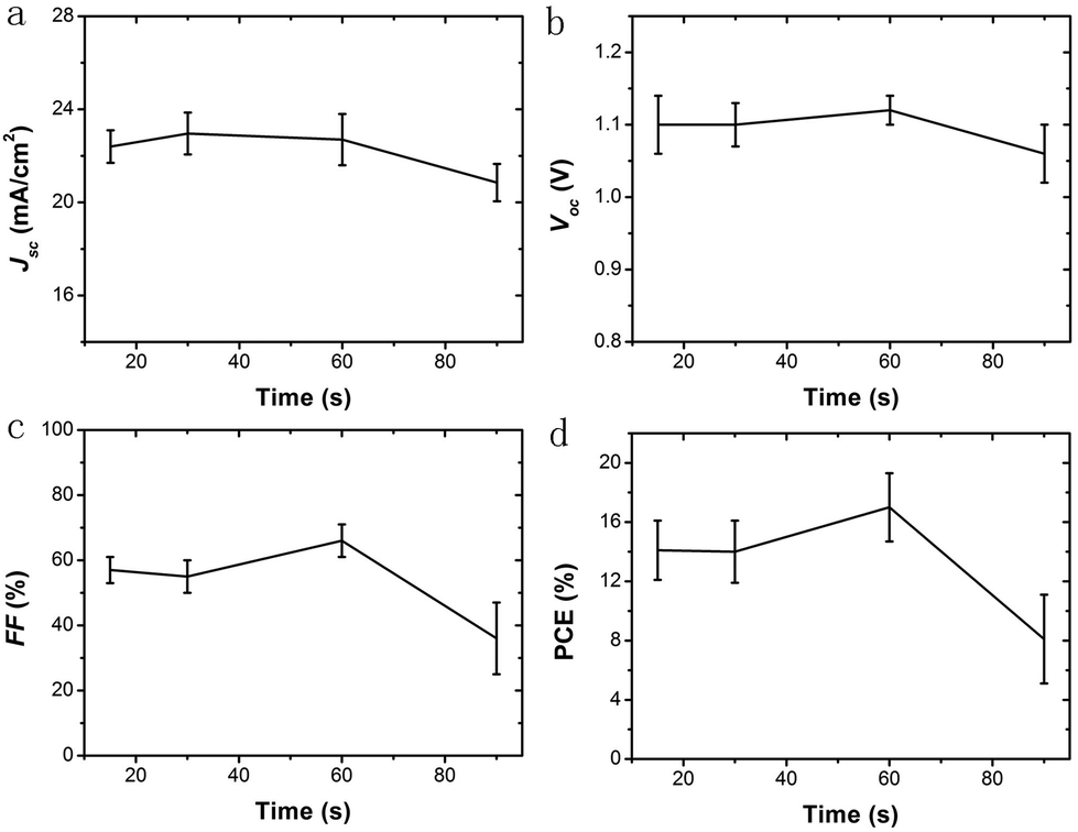 | ||
| Fig. 5 Main photovoltaic parameters. (a) Jsc, (b) Voc, (c) FF and (d) PCE for PSCs based on different collecting periods of TiO2 NHSs (15 s, 30 s, 60 s and 90 s). 20 devices are made and tested for each collecting period. | ||
This is attributed to the different electron transporting mechanisms within TiO2/perovskite heterojunctions, under different TiO2 NHS distribution density conditions, as demonstrated in Fig. 6 (the NHS structure can be clearly seen in Fig. S3a†). To be more specific, for the collecting period of 15 s, 30 s and 60 s, the population of TiO2 NHSs is small in relative terms of the substrate area, so most of the TiO2 NHSs are evenly distributed and are in a monodisperse state as plotted in Fig. 6a–c (the SEM image of 30 s and 60 s collected TiO2 NHSs is shown in Fig. S3b and S3c†). In this case, photoinduced electrons generated in the perovskite tend to inject into the CB of the nearest TiO2 NHS, as illustrated in Fig. 6e. Electrons transport/inject more efficiently into the TiO2 CB with more TiO2 NHSs. Also, the hysteresis effect is significantly minimized within more mesoporous TiO2 nanostructures.11–13 Thus an enhanced Jsc and FF can be obtained in the PSC-60 s. But when the TiO2 NHSs accumulate after a longer time (90 s in this case) when the density becomes relatively large, as illustrated in Fig. 6d and f (the SEM image of 90 s collected TiO2 NHSs is shown in Fig. S3d†), TiO2 NHSs pile up which lead to some non-direct contacts between TiO2 NHSs and the FTO/TiO2 compact layer substrate. In this case, some photogenerated electrons have to pass through the interface between upper and lower TiO2 NHSs before they can finally reach the FTO. As a consequence, the distance, in which electrons need to transport to the substrate, is extended and more free electrons may be annihilated during this period,9,12,13 which lead to a reduction in the number of electrons that finally reach FTO. Therefore, the performance of the PSC-90 s is worse than that of the PSC-60 s. And for the same reason, the IPCE curves of the PSCs shown in Fig. 4d remain at a similar level when the collecting time is below 60 s, and drop evidently when the collecting time increases to 90 s.
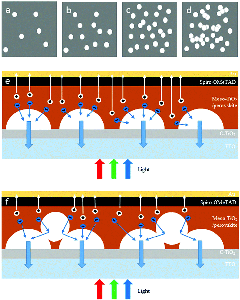 | ||
| Fig. 6 Schematic drawing of the TiO2 NHS dispersion with different collecting times. NHSs distribution status with a collecting time of (a) 15 s, (b) 30 s, (c) 60 s, and (d) 90 s, respectively, and cross-section schematics for the collecting time of (e) 60 s and (f) 90 s. | ||
As a comparison, anatase TiO2 NPs prepared by the same hydrothermal method are used in the PSCs with an identical device configuration and fabrication process to the TiO2 NHSs, as shown in Fig. 1. Fig. 7a plots the J–V curves for the corresponding champion devices based on both TiO2 NHSs and TiO2 NPs. It is apparent that most of the photovoltaic parameters of the TiO2 NHS based device, including Voc (1.14 V), Jsc (23.8 mA cm−2) and FF (0.71), are superior to the corresponding data (Voc of 1.12 V, Jsc of 22.2 mA cm−2 and FF of 0.68) of the TiO2 NP counterpart. Thus, the TiO2 NHS based device generates a PCE of 19.3%, which is better than the 17.0% efficiency provided by the TiO2 NP based device. For the IPCE curves as shown in Fig. 7b, there is an obvious enhancement response in the wavelength range from 500 nm to 760 nm. This enhancement may be related to an optical interference effect caused by TiO2 NHS arrays. For λ > 500 nm the cavity of PSC operates in the low-finesse thin-film interference regime,41 so the TiO2 NHS arrays with the dimension of sub-wavelength may cause the interference of input light and generate optical field enhancement within the perovskite layer, which will lead to more efficient light absorption. The FDTD42 simulations show the difference of optical power distribution at the TiO2/perovskite interface between the NP based model and NHS (60 s) based model (Fig. S4a and S4b†), which indicates the effect of optical interference. Optical absorption spectra also show the enhanced light absorption in the FTO/C-TiO2/TiO2 NHSs 60 s/perovskite sample (Fig. S4c†). Furthermore, little hysteresis11–13 is found in the J–V curve of the champion device of PSC-60 s (Fig. S5†). A preliminary stability investigation of these PSCs has been performed for 60 days, which shows that the devices stored in the dark at room temperature are relatively stable, with just a 0.7% PCE drop in the entire testing period (Table S1†).
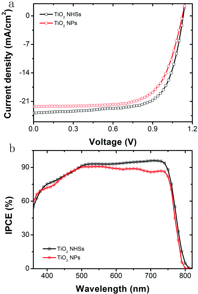 | ||
| Fig. 7 (a) J–V curves and (b) IPCE spectra of champion devices fabricated based on TiO2 NHSs and the control group based on TiO2 NPs. | ||
To study the photogenerated free carrier behaviour in the PSC based on 60 s collected TiO2 NHSs, small perturbation TPV is utilized to observe the fast decay component occurrence within the system with the time relaxation constant in the nanosecond (ns) scale.43–45 Thus, we operate complementary small perturbation TPVs by using a white light source to vary the back illumination level and a ns-pulsed 532 nm Nd/YAG laser to induce the small voltage perturbations and the results are shown in Fig. 8a. The TPVs show one component of the photovoltage decays, a lifetime that spans from 102 to 174 μs in a wide back illumination level from 0.8 V to 0.2 V (as summarized in Table S2†), which is much longer than its mesoporous TiO2 NP counterpart (only 4 μs in the back level of 1 V, shown in Fig. S6†). This is ascribed to the increase of the contact area between FA0.81MA0.15Pb(I0.836Br0.15)3 and TiO2. Also, the use of TiO2 NHSs can further optimize the device structure to obtain an optimal combination of the series resistance and shunt resistance. Thus, the free carriers can transport a longer distance in this TiO2 NHSs/FA0.81MA0.15Pb(I0.836Br0.15)3 heterojunction and this TiO2 NHS layer is indeed a good replacement to its predecessor-mesoporous TiO2 NP layer in the application of efficient PSCs. Moreover, the obtained lifetime is much longer than that in the typical TiO2 NP based CH3NH3PbI3 solar cell (3 to 92 μs with the back illumination level 0.7 V to 0.1 V).45 As a result, the free carriers are able to transport a longer distance in this FA0.81MA0.15Pb(I0.836Br0.15)3 light absorbing layer, compared to the CH3NH3PbI3 layer.
 | ||
| Fig. 8 (a) Normalized small perturbation TPVs of the PSC. (b) TOF hole transients and mobilities measured at different back voltages for the device. (c) TOF electron transients and mobilities measured at different back voltages for the device. | ||
Charge mobility in this device is also studied with a TOF photoconductivity technique at room temperature.46,47 By simply changing the applied background voltages of the device, the electron and hole transit time can be obtained separately. Furthermore, the electron and hole mobilities of the system can be easily calculated, given the heterojunction thickness, applied back voltage and free charge transit time. Fig. 8b shows the TOF hole transients and mobilities for laser generated holes obtained at different external applied voltages (the full spectra can be found in Fig. S7†). The transit time can be obtained from the peak of the TOF transients spectra and the charge mobility (μ) in the system can be further calculated with the relation μ = d2/VtT,46,47 where d is the perovskite/HTM thickness (650 nm), V is the applied voltage, and tT is the transit time. The calculated hole mobility in the FA0.81MA0.15Pb(I0.836Br0.15)3/spiro-OMeTAD heterojunction under ambient conditions is 4.0 × 10⁻³ cm2 V−1 s−1, which is one order of magnitude higher than that in the CH3NH3PbI3/spiro-OMeTAD heterojunction (∼10−4 cm2 V−1 s−1)48 and 4 times higher than that in the typical mesoporous TiO2 NP based FA0.81MA0.15Pb(I0.836Br0.15)3 PSC (1.0 × 10⁻³ cm2 V−1 s−1, as shown in Fig. S8†), with an external applied electric field of 1.33 × 10⁴ V cm−1. We found that the mobility values of free photogenerated holes are all above 10−3 cm2 V−1 s−1 within the whole voltage range. The TOF transients and mobilities for photoinduced free electrons with different applied background voltages are shown in Fig. 8c. In this work, the electron mobility in the system is 2.4 × 10⁻³ cm2 V−1 s−1 at an applied electric field of 1.54 × 10⁴ V cm−1 for a 650 nm thick TiO2/FA0.81MA0.15Pb(I0.836Br0.15)3 heterojunction. The electron mobility values are around 10−3 cm2 V−1 s−1 within the 1–5 V voltage range, which is nearly one order of magnitude higher than that in the typical mesoporous TiO2 NP based FA0.81MA0.15Pb(I0.836Br0.15)3 PSC (∼10−4 cm2 V−1 s−1). The electron mobility in the device is slightly smaller than the hole mobility and this mobility mismatch of electrons and holes may influence the overall performance of the device, thus interface modifying such as metal ion doping and coating as well as the surface plasmonic effect of metal nanoparticles can be used to further increase the efficiency of this kind of PSC.38,49–53
Conclusions
In summary, we have exploited an electrospray method using hydrothermally synthesized TiO2 NP suspension solution to fabricate TiO2 NHSs with an average radius of ∼200 nm. The TiO2 NHSs have been further employed as a mesoporous layer of FA0.81MA0.15Pb(I0.836Br0.15)3 based PSCs. Detailed electron transporting mechanisms are discussed based on the difference of TiO2 NHS distribution densities with various electrospraying collecting periods. The PSC with the collecting period of 60 s demonstrates an optimized 19.3% PCE with a Jsc of 23.8 mA cm−2, a Voc of 1.14 mV and a FF of 0.71, which is superior to the TiO2 NP based control group with the PCE of 17.0%. TPV measurement indicates that PSC-60 s, compared to the PSC adopting 30 nm TiO2 NPs, exhibits notably efficient carrier injection/transport from FA0.81MA0.15Pb(I0.836Br0.15)3 to both TiO2 NHS and HTM layers. This is due to the increase of the contact area between FA0.81MA0.15Pb(I0.836Br0.15)3 and TiO2 caused by this unique TiO2 NHS network and the optimized overall device structure. Moreover, the TOF results show that the photogenerated free carrier mobilities in the proposed system are higher than the TiO2 NP based PSC.Acknowledgements
This work is supported by the Singapore-Berkeley Energy Research Institute (SinBeRISE), Grantor Lloyd's Register Foundation (R-265-000-553-597), the Singapore Ministry of Education Academic Research Fund Tier 2 (MOE2015-T2-1-066, MOE2015-T2-2-010), and Nanyang Technological University (Start-up grant: Lei Wei). The authors thank Dr Xizu Wang, Dr Changyun Jiang, Dr Lim Siew Lay and Mr Goh Wei Peng from IMRE for fruitful discussion and access to the glovebox.Notes and references
- National Renewable Energy Laboratory (NREL), Research Cell Efficiency Records, http://www.nrel.gov/ncpv/images/efficiency_chart.jpg, accessed: November, 2016.
- A. Kojima, K. Teshima, Y. Shirai and T. Miyasaka, J. Am. Chem. Soc., 2009, 131, 6050 CrossRef CAS PubMed.
- J.-H. Im, C.-R. Lee, J.-W. Lee, S.-W. Park and N.-G. Park, Nanoscale, 2011, 3, 4088 RSC.
- H. S. Kim, C. R. Lee, J. H. Im, K. B. Lee, T. Moehl, A. Marchioro, S. J. Moon, R. Humphry-Baker, J. H. Yum, J. E. Moser, M. Gratzel and N. G. Park, Sci. Rep., 2012, 2, 591 Search PubMed.
- J. H. Heo, S. H. Im, J. H. Noh, T. N. Mandal, C.-S. Lim, J. A. Chang, Y. H. Lee, H.-J. Kim, A. Sarkar, M. K. Nazeeruddin, M. Grätzel and S. I. Seok, Nat. Photonics, 2013, 7, 486 CrossRef CAS.
- M. M. Lee, J. Teuscher, T. Miyasaka, T. N. Murakami and H. J. Snaith, Science, 2012, 338, 643 CrossRef CAS PubMed.
- J. Burschka, N. Pellet, S. J. Moon, R. Humphry-Baker, P. Gao, M. K. Nazeeruddin and M. Grätzel, Nature, 2013, 499, 316 CrossRef CAS PubMed.
- T. Leijtens, G. E. Eperon, S. Pathak, A. Abate, M. M. Lee and H. J. Snaith, Nat. Commun., 2013, 4, 2885 Search PubMed.
- H. Zhou, Q. Chen, G. Li, S. Luo, T. B. Song, H. S. Duan, Z. Hong, J. You, Y. Liu and Y. Yang, Science, 2014, 345, 542 CrossRef CAS PubMed.
- W. S. Yang, J. H. Noh, N. J. Jeon, Y. C. Kim, S. Ryu, J. Seo and S. I. Seok, Science, 2015, 348, 1234 CrossRef CAS PubMed.
- D. Bi, W. Tress, M. I. Dar, P. Gao, J. Luo, C. Renevier, K. Schenk, A. Abate, F. Giordano, J. P. Baena, J. D. S. M. Zakeeruddin, M. K. Nazeeruddin, M. Grätzel and A. Hagfeldt, Sci. Adv., 2016, 2, e1501170 Search PubMed.
- D. Zhong, B. Cai, X. Wang, Z. Yang, S. Miao, W. H. Zhang and C. Li, Nano Energy, 2015, 11, 409 CrossRef CAS.
- I. S. Yang, J. S. You, S. D. Sung, C. W. Chung, J. Kim and W. I. Lee, Nano Energy, 2016, 20, 272 CrossRef CAS.
- N. J. Jeon, J. H. Noh, W. S. Yang, Y. C. Kim, S. Ryu, J. Seo and S. I. Seok, Nature, 2015, 517, 476 CrossRef CAS PubMed.
- Z. Xiao, Y. Yuan, Y. Shao, Q. Wang, Q. Dong, C. Bi, P. Sharma, A. Gruverman and J. Huang, Nat. Mater., 2015, 14, 193 CrossRef CAS PubMed.
- H.-S. Kim, S. H. Im and N.-G. Park, J. Phys. Chem. C, 2014, 118, 5615 CAS.
- G. Murugadoss, G. Mizuta, S. Tanaka, H. Nishino, T. Umeyama, H. Imahori and S. Ito, APL Mater., 2014, 2, 081511 CrossRef.
- S. D. Sung, D. P. Ojha, J. S. You, J. Lee, J. Kim and W. I. Lee, Nanoscale, 2015, 7, 8898 RSC.
- N. Y. Ahn, D. Y. Son, I. H. Jang, S. M. Kang, M. S. Choi and N. G. Park, J. Am. Chem. Soc., 2015, 137, 8696 CrossRef CAS PubMed.
- D. Hwang, H. Lee, S. Y. Jang, S. M. Jo, D. Kim, Y. Seo and D. Y. Kim, ACS Appl. Mater. Interfaces, 2011, 3, 2719 CAS.
- H. Lee, D. Hwang, S. M. Jo, D. Kim, Y. Seo and D. Y. Kim, ACS Appl. Mater. Interfaces, 2012, 4, 3308 CAS.
- A. Léaustic, F. Bahonneau and J. Livage, Chem. Mater., 1989, 1, 248 CrossRef.
- X. Jiang, T. Herricks and Y. Xia, Adv. Mater., 2003, 15, 1205 CrossRef CAS.
- S. Eiden-Assmann, J. Widoniak and G. Maret, Chem. Mater., 2004, 16, 6 CrossRef CAS.
- J. H. Pan, Q. Wang and D. W. Bahnemann, Catal. Today, 2014, 230, 197 CrossRef CAS.
- D. Chen, F. Huang, Y.-B. Cheng and R. A. Caruso, Adv. Mater., 2009, 21, 2206 CrossRef CAS.
- Y. J. Kim, M. H. Lee, H. J. Kim, G. Lim, Y. S. Choi, N.-G. Park, K. Kim and W. I. Lee, Adv. Mater., 2009, 21, 3668 CrossRef CAS.
- I. G. Yu, Y. J. Kim, H. J. Kim, C. Lee and W. I. Lee, J. Mater. Chem., 2011, 21, 532 RSC.
- S. H. Jang, Y. J. Kim, H. J. Kim and W. I. Lee, Electrochem. Commun., 2010, 12, 1283 CrossRef CAS.
- W.-Y. Cheng, J. R. Deka, Y.-C. Chiang, A. Rogeau and S.-Y. Lu, Chem. Mater., 2012, 24, 3255 CrossRef CAS.
- H.-E. Wang, L.-X. Zheng, C.-P. Liu, Y.-K. Liu, C.-Y. Luan, H. Cheng, Y. Y. Li, L. Martinu, J. A. Zapien and I. Bello, J. Phys. Chem. C, 2011, 115, 10419 CAS.
- R. Zhou, Q. Zhang, E. Uchaker, J. Lan, M. Yin and G. Cao, J. Mater. Chem. A, 2014, 2, 2517 CAS.
- X.-Y. Yu, J.-Y. Liao, K.-Q. Qiu, D.-B. Kuang and C.-Y. Su, ACS Nano, 2011, 5, 9494 CrossRef CAS PubMed.
- T. Shu, P. Xiang, Z.-M. Zhou, H. Wang, G.-H. Liu, H.-W. Han and Y. D. Zhao, Electrochim. Acta, 2012, 68, 166 CrossRef CAS.
- S. D. Sung, I. Lim, P. Kang, C. Lee and W. I. Lee, Chem. Commun., 2013, 49, 6054 RSC.
- Y.-F. Xu, W.-Q. Wu, H.-S. Rao, H.-R. Chen, D.-B. Kuang and C.-Y. Su, Nano Energy, 2015, 11, 621 CrossRef CAS.
- T. Leijtens, B. Lauber, G. E. Eperon, S. D. Stranks and H. J. Snaith, J. Phys. Chem. Lett., 2014, 5, 1096 CrossRef CAS PubMed.
- J. T. Wang, J. M. Ball, E. M. Barea, A. Abate, J. A. Alexander-Webber, J. Huang, M. Saliba, I. Mora-Sero, J. Bisquert, H. J. Snaith and R. J. Nicholas, Nano Lett., 2013, 14, 724 CrossRef PubMed.
- H. Cheng, J. Ma, Z. Zhao and L. Qi, Chem. Mater., 1995, 7, 663 CrossRef CAS.
- A. Testino, I. R. Bellobono, V. Buscaglia, C. Canevali, M. D'Arienzo, S. Polizzi, R. Scotti and F. Morazzoni, J. Am. Chem. Soc., 2007, 129, 3564 CrossRef CAS PubMed.
- Q. Lin, A. Armin, R. C. Nagiri, P. L. Burn and P. Meredith, Nat. Photonics, 2015, 9, 106 CrossRef CAS.
- K. S. Yee, IEEE Trans. Antennas Propag., 1966, 14, 302 CrossRef.
- S. D. Stranks, V. M. Burlakov, T. Leijtens, J. M. Ball, A. Goriely and H. J. Snaith, Phys. Rev. Appl., 2014, 2, 034007 CrossRef.
- V. Roiati, S. Colella, G. Lerario, L. De Marco, A. Rizzo, A. Listorti and G. Gigli, Energy Environ. Sci., 2014, 7, 1889 CAS.
- L. Bertoluzzi, R. S. Sanchez, L. Liu, J. W. Lee, E. Mas-Marza, H. Han, N. G. Park, I. Mora-Sero and J. Bisquert, Energy Environ. Sci., 2015, 8, 910 CAS.
- Q. Dong, Y. Fang, Y. Shao, P. Mulligan, J. Qiu, L. Cao and J. Huang, Science, 2015, 347, 967 CrossRef CAS PubMed.
- M. J. Tan, W. P. Goh, J. Li, G. Pundir, V. Chellappan and Z. K. Chen, ACS Appl. Mater. Interfaces, 2010, 2, 1414 CAS.
- D. Bi, L. Yang, G. Boschloo, A. Hagfeldt and E. M. Johansson, J. Phys. Chem. Lett., 2013, 4, 1532 CrossRef CAS PubMed.
- W. Guo, C. Xu, X. Wang, S. Wang, C. Pan, C. Lin and Z. L. Wang, J. Am. Chem. Soc., 2012, 134, 4437 CrossRef CAS PubMed.
- H. Park, Y. Park, W. Kim and W. Choi, J. Photochem. Photobiol., C, 2013, 15, 1 CrossRef CAS.
- W. Zhang, M. Saliba, S. D. Stranks, Y. Sun, X. Shi, U. Wiesner and H. J. Snaith, Nano Lett., 2013, 13, 4505 CrossRef CAS PubMed.
- F. Giordano, A. Abate, J. P. Baena, M. Saliba, T. Matsui, S. H. Im, S. M. Zakeeruddin, M. K. Nazeeruddin, A. Hagfeldt and M. Graetzel, Nat. Commun., 2016, 9, 1989 Search PubMed.
- W. E. Zhang, M. Saliba, S. D. Stranks, Y. Sun, X. Shi, U. Wiesner and H. J. Snaith, Nano Lett., 2013, 13, 4505 CrossRef CAS PubMed.
Footnotes |
| † Electronic supplementary information (ESI) available. See DOI: 10.1039/c6nr07369g |
| ‡ These authors contributed equally to this work. |
| This journal is © The Royal Society of Chemistry 2017 |