
 Open Access Article
 This Open Access Article is licensed under a
 Creative Commons Attribution 3.0 Unported Licence
Single-electron tunneling through an individual arsenic dopant in silicon
V. V.
Shorokhov
 a,
D. E.
Presnov
a,
S. V.
Amitonov
a,
Yu. A.
Pashkin
*bc and
V. A.
Krupenin
a
a,
D. E.
Presnov
a,
S. V.
Amitonov
a,
Yu. A.
Pashkin
*bc and
V. A.
Krupenin
a
aM.V. Lomonosov Moscow State University, Moscow 119991, Russia
bDepartment of Physics, Lancaster University, Lancaster LA1 4YB, UK. E-mail: y.pashkin@lancaster.ac.uk
cLebedev Physical Institute, Moscow 119991, Russia
First published on 24th November 2016
Abstract
We report the single-electron tunneling behaviour of a silicon nanobridge where the effective island is a single As dopant atom. The device is a gated silicon nanobridge with a thickness and width of ∼20 nm, fabricated from a commercially available silicon-on-insulator wafer, which was first doped with As atoms and then patterned using a unique CMOS-compatible technique. Transport measurements reveal characteristic Coulomb diamonds whose size decreases with gate voltage. Such a dependence indicates that the island of the single-electron transistor created is an individual arsenic dopant atom embedded in the silicon lattice between the source and drain electrodes, and furthermore, can be explained by the increase of the localisation region of the electron wavefunction when the higher energy levels of the dopant As atom become occupied. The charge stability diagram of the device shows features which can be attributed to adjacent dopants, localised in the nanobridge, acting as charge traps. From the measured device transport, we have evaluated the tunnel barrier properties and obtained characteristic device capacitances. The fabrication, control and understanding of such “single-atom” devices marks a further step towards the implementation of single-atom electronics.
1. Introduction
The remarkable progress of semiconductor industry based on advances in the fabrication of silicon CMOS devices has led to high-speed, ultra-dense and low cost integrated circuits that we use today in our gadgets. The characteristic feature size of semiconductor devices has shrunk to 22 nm (ref. 1) in which only a small number of dopant states contribute to the current, and it is expected that in the near future the feature size will approach the minimum possible size – that of a single atom. It was realized that a new class of electronic devices can be envisaged that have solitary dopants as key elements.The change of the paradigm for dopants from being passive charge providers in semiconductor microelectronic devices to becoming key elements of single-atom functional devices may have a great impact on future nanoelectronics by advancing both conventional and quantum circuits for information processing, sensing and metrology applications.2,3
The use of individual atoms as building blocks of nanoelectronic devices is a very attractive idea, since atoms possess a stable electronic structure and well-defined properties. An important property of individual atoms embedded in a medium is that their quantum confinement energy is of the order of the Coulomb energy, which allows the fabrication of unique single-atom single-electron tunneling devices as prototypes of quantum bits,4–6 quantum logic gates7 required for building a quantum processor, logic gates for conventional computers,8 and charge pumps for quantum metrology.9,10 Individual dopants in the Si medium were accessed using advanced characterization techniques including tunneling spectroscopy with gated nanowires11–16 and scanning probe structures,17,18 microwave assisted tunneling19 capacitance spectroscopy20 and RF reflectometry.21
Single-dopant-based electronic devices have entered the era of active development, therefore understanding the single-impurity physics and establishment of reliable fabrication methods for such devices would be an important milestone on the way to building integrated circuits made of solitary atoms and molecules. A major goal on this path is to find an optimal combination of a semiconductor and a dopant atom in order to build a transistor with ultimate performance, that is, a high Coulomb energy and therefore a high operating temperature. Here we demonstrate one of the possible ways to realize a single-atom device using a combination of well-controlled ion implantation, electron-beam lithography and reactive ion etching.
1.1. The physics of the As single-atom single-electron tunneling transistor
The key idea in the description of the donor atom placed in a host medium is that one more valence electron than the host semiconductor has ground and excited states corresponding to the Rydberg series of the free hydrogen atom.22 Under these assumptions, the donor electron will have hydrogen-like bound states given by| En = −m*e4/ħ2ε2n2, | (1) |
A key requirement to the nanobridge connecting the source and drain electrodes in the transistor is that its material must be an extrinsic semiconductor with a high degree of doping (1018–1019 cm−3). For the electron transport to be in the weak-coupling limit, also known as the single-electron tunneling regime,26 the tunneling conductance between a pair of dopants should be G = (10−4–10−2)G0, where G0 = e2/h is the conductance quantum. Ideally, the narrowest part of the nanobridge should contain no more than one dopant, which can be satisfied for the constriction of width/thickness ∼10 nm and a dopant concentration not exceeding 1019 cm−3. A device in which the metallic island is replaced by a single dopant was nicknamed the ‘single-atom transistor’.6
Fig. 1a shows a schematic diagram of the device in which the island is represented by an individual dopant in the nanobridge, which is tunnel coupled to the electrodes formed by dopants with higher concentration. The electrodes possess metal-like properties with the electron distribution obeying the Fermi–Dirac statistics. Such a device can be modelled as a single-electron transistor with capacitances CL, CR and CG and tunneling rates ΓL and ΓR, as shown in the inset of Fig. 1a, whose island has an energy spectrum determined by the dopant properties.
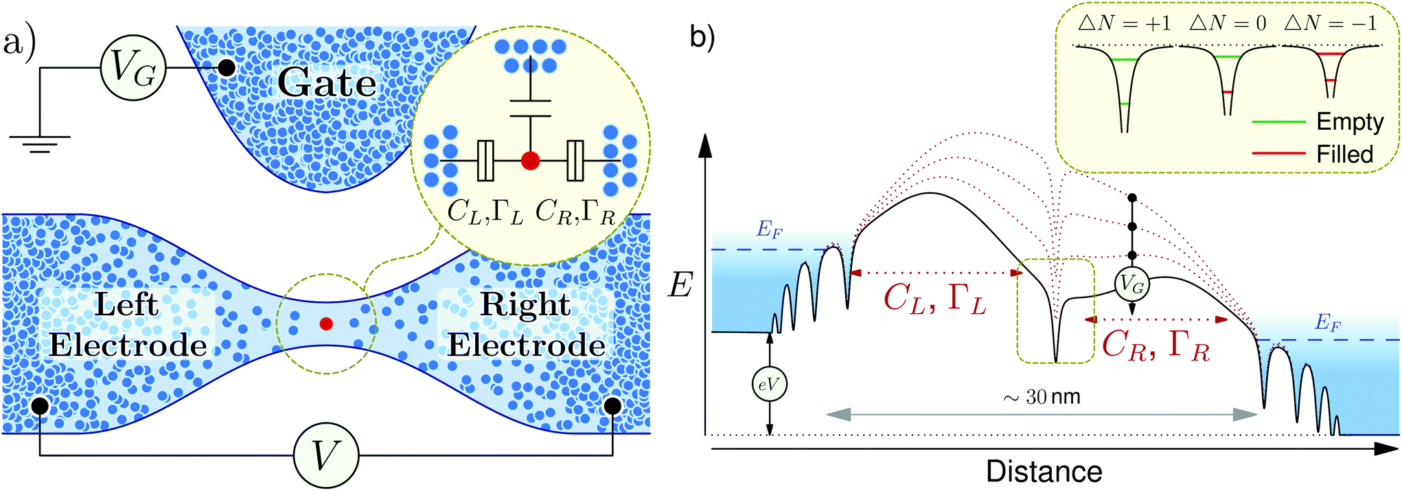 | ||
| Fig. 1 (a) Schematic view of the planar single-atom single-electron transistor. As dopants are shown as blue dots. Inset: Equivalent circuit diagram of the transistor central part. The dopant indicated by the red dot is modelled as an island with capacitance C that is tunnel coupled to the source and drain electrodes whose potential is controlled by a nearby gate. (b) Schematics of the nanobridge potential profile for fixed bias voltage and its evolution under the application of the positive gate voltages. The profile and the dopant potential wells are not to scale. Inset: Schematics of the dopant single-particle energy spectra for three charge configurations. The red lines correspond to the states occupied by electrons, the green lines are empty states. The dopant energy levels shift under the application of V and VG. | ||
The potential profile of the device is presented in Fig. 1b. The electrodes with a higher dopant concentration are shown as metals with Fermi levels EF controlled by a bias voltage, V. The presence of a dopant creates a potential dip in the profile, with two tunnel barriers formed between the dopant and the electrodes. The figure also shows the evolution of the potential profile and tunnel barriers under the application of a gate voltage, VG, with an arrow indicating the shift under four positive voltages. The positive gate voltage also shifts the single-particle dopant energy levels further into the energy gap and increases the number of electrons on the dopant, while the negative gate voltage shifts them into the conduction band and leads to fewer electrons on the dopant, as indicated in the inset.
The application of bias voltage results in the distortion of the bottom of the conduction band and hence shifts of the potential barriers with respect to each other. The shape of the resulting potential barrier between the dopant and the electrodes depends strongly on the depth of the energy levels and the applied bias and gate voltages. Charging and discharging of the dopant affects its energy spectrum as shown in the inset of Fig. 1b. The increase in the number of electrons on the dopant site makes the potential well shallower and hence the number of vacant single-particle energy levels and spacing between them decreases. In contrast, the reduction in the number of electrons leads to a deeper potential well and a greater number of vacant energy levels and separation between them. The tunnel barrier through which charge carriers tunnel from the dopant center to the electrodes has a height that is determined by the energy difference between the bottom of the conduction band and the corresponding donor level for the electrons or the top of the valence band and the acceptor level for the holes.
2. Fabrication of the As single-atom single-electron tunneling transistor
To fabricate the As single-atom transistor, we used the so-called top-down approach that included creation of the desired doping profile in the top Si layer of a silicon-on-insulator (SOI) wafer, its patterning using electron-beam lithography to create all components of the transistor including a nanobridge, and fine trimming of the nanobridge by reactive ion etching to have a single isolated dopant atom in the constriction. The newly developed fabrication process is fully CMOS-compatible and more details are presented below. The key advantage of our approach is that the whole structure is patterned in a single layer of doped Si leaving the nanobridge open and free from the detrimental effects of the interfacing layers usually formed between the nanobridge and the top gate. Such an open device architecture allows its use in sensing applications. More details on the fabrication process are presented below.Commercially available SOI wafers had a 55 nm thick top Si layer with a resistivity of 10 Ω cm. It was isolated from the 725 μm thick Si wafer with the same resistivity by a 145 nm thick layer of SiO2. The top Si layer, the active layer, in which the transistor was patterned, was implanted by ions almost to the solubility limit of the dopant atoms in Si. To minimize the thickness of the highly doped layer, heavy ions, As+, were used at a low acceleration voltage, 6 kV, and a total dose of 1.25 × 1015 cm−2. This process created a dopant concentration profile shown by the blue line in Fig. 2. To restore the crystal structure of Si after the ion implantation, rapid thermal annealing was performed at a temperature of 925 °C for 10 s, which resulted in the redistribution of dopants within the Si layer, as shown by the red line in Fig. 2. As a result, the top 30 nm of the Si layer was doped up to the degeneracy level of 1019–1020 cm−3 and had a quasi-metallic conductivity. At the same time, the dopant concentration of the bottom of the active Si layer decreased down to ∼1017 cm−3. The sheet resistance of the active SOI layer was measured to be ∼300 Ω sq−1.
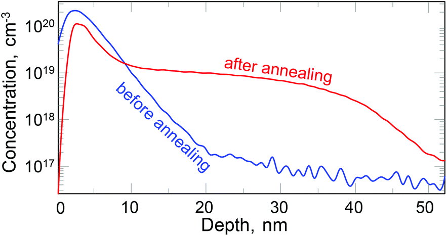 | ||
| Fig. 2 Measured concentration of As dopants in the active Si layer as a function of depth before and after thermal annealing. The annealing process facilitates the penetration of the dopant atoms deeper into the Si lattice. The region with a moderate slope on the red curve enables fine control of the dopant number in the nanobridge by using short dry etching steps, and eventually reduces the number to one. | ||
The patterning of the active Si layer was performed by electron-beam lithography using a scanning electron microscope Supra40 (Carl Zeiss) equipped with a beam blanker and a pattern generator ELPHY Quantum (RAITH). To define the transistor structure, a desired pattern was drawn in the layer of the electron-beam resist PMMA 950K, which was prepared and processed using a standard recipe. After the resistance development, a 10 nm thick Al film was deposited, which was followed by a lift-off process. Next, this metal layer was used as a mask during anisotropic reactive ion etching of the active Si layer in CF4 plasma and later removed in a weak alkaline solution.
Top and side views of the transistor structure obtained using a scanning electron microscope are shown in Fig. 3a and b. We believe that due to a small asymmetry, only one of the two nanobridges contains an individual dopant atom that was incorporated into the crystal structure during ion implantation, which is indicated by the red dot. This atom functions as an active charge center, which is an analog of the island or quantum dot in various types of single-electron transistors, whose potential is controlled by a nearby gate.26–32 The dopant center is tunnel coupled to the source and drain electrodes that are patterned together with the gate in the same conducting layer of highly doped Si.
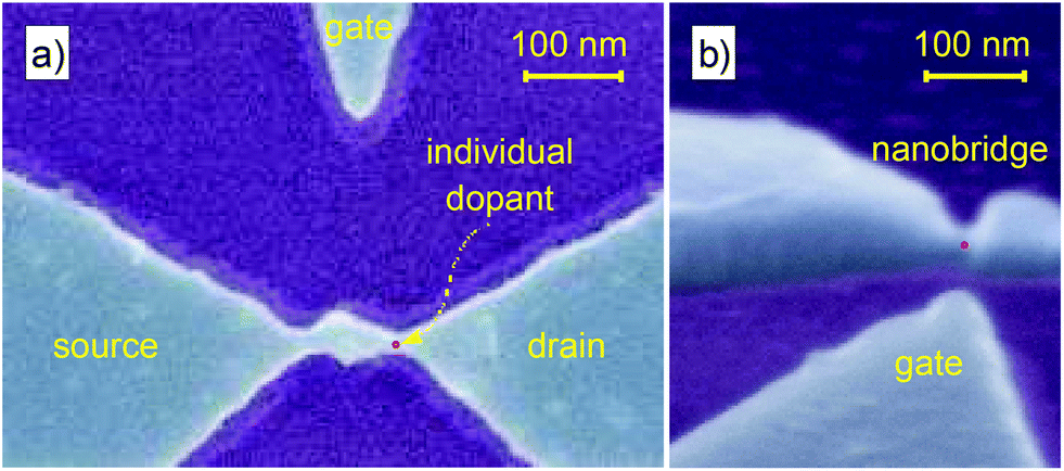 | ||
| Fig. 3 False color top (a) and side (b) view of the SOI-based device observed using the scanning electron microscope. The top view depicts an overall layout of the device containing two nanobridges with a reduced dopant concentration due to the smaller thickness as compared to the rest of the structure. The profile of the transistor is clearly seen in the side view. An individual isolated dopant is indicated by the red dot. | ||
3. Results and discussion
Before measuring the single-atom transistor in detail at 4.2 K, we tested several devices at 77 K and selected those that exhibited an offset of the current–voltage (I–V) characteristics at a high bias, |V| ≥ 10 mV, and a reasonable stability diagram. The final trimming of the fabricated structures was performed by reactive ion etching in CF4 for about 10 s for a few times and monitoring the sample resistance and voltage offset at 77 K after each etching step. The consecutive short etching steps used resulted in the gradual and controlled reduction of the number of current peaks in the stability diagram. When the quadruple, triple and double peaks disappeared in the stability diagram, the sample was characterized at 4.2 K. We believe the reduction of the current peak number corresponds to the smaller number of dopants in the nanobridge and eventually charge transport takes place through a single isolated dopant producing a stability diagram shown in Fig. 4. A similar reduction of the number of current peaks in the stability diagram was observed in ref. 16. | ||
| Fig. 4 Stability diagram measured in a wide range of V and VG. The absolute value of the measured current |I| is used to contrast the diagram. The leftmost Coulomb diamond with VG up to about 10 V corresponds to the positively charged dopant. The dopant becomes neutral at higher VG. The region of high VG corresponds to the negatively charged dopant. | ||
The stability diagram in Fig. 4 is plotted for the absolute value of the tunnel current |I| as a function of V and VG in the range V = ± 120 mV and VG = 0–70 V, with VG = 70 V being the highest gate voltage before the electrical breakdown occurred. The I–V curves were measured at VG = 0 V first, and then VG was increased with an increment of 1 V. The stability diagram consists of characteristic diamonds in which the current is suppressed, and the triangle-shaped areas corresponding to the finite current, the current triangles.
The blockade voltage of the Coulomb diamonds, as seen in the diagram, decreases at higher gate voltages, which was also observed in several earlier studies.6,11–14 The different sizes of the Coulomb diamonds in this figure correspond to the different charging energies and hence different effective self-capacitances of atomic subshells localized on the dopant. Higher single-particle energy levels correspond to larger self and mutual capacitances.
The observed stability diagram can be interpreted as follows. At V = 0 and VG = 0 the valence electron in the first atomic shell of the As dopant is delocalized, which corresponds to the charge state ΔN = +1. Therefore, when VG is increased, the first current triangle corresponds to electron transport between ΔN = +1 and ΔN = 0 charge states through the first single-particle energy level of the dopant. As the gate voltage increases, the dopant average charge changes corresponding to the most probable electronic configurations of the dopant. In the stability diagram in Fig. 4, four characteristic sizes of Coulomb diamonds can be identified that correspond to different dopant single-particle orbitals.
From this diagram, using the orthodox theory of single-electron tunneling,26,33 we obtained the characteristic charging energy, the bias division factor and the single-particle excitation spectrum.
The observed smearing and ragged edges can be attributed to the influence of the adjacent donors acting as charge traps, which are activated by the high temperature (4.2 K) used in the experiment. One can see that the charge traps have stronger effects on the dopant at a higher gate voltage, which can be attributed to their activation by VG and also the decrease of their charging energy when they accumulate more electrons.
Overall, the large-scale picture of the stability diagram is dominated by a single dopant presumably located in the narrower nanobridge, while the distortions and imperfections are caused by the surrounding dopants.
To have a deeper insight into the charge transport through the dopant, the stability diagram was measured at low V and VG (Fig. 5). The current triangle defined by lines α and ε shown in Fig. 5b corresponds to the leftmost current triangle in Fig. 4, but shifted to lower VG due to the effect of offset charge. Importantly, at low bias and gate voltages, there are almost no distortions (jumps and shifts) of the stability diagram, caused by the surrounding dopants, which only introduce small fluctuations in the position of the tunnel current steps.
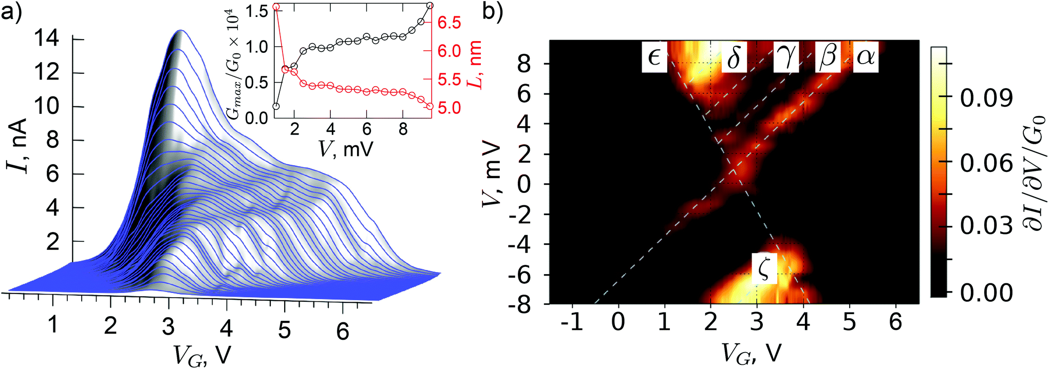 | ||
| Fig. 5 Stability diagram measured at low bias and gate voltages. Steps of the tunnel current seen in (a) are marked by Greek letters and dashed lines in (b). Such steps are caused by the dopant discrete energy spectrum. (Inset) Gmax/G0 for the α line and effective tunnel barrier length L as functions of V obtained from the measured data. | ||
To estimate the dopant charging energy, we used a table value of 54 meV for the As ground state energy level.34 The slopes of the current triangle boundaries in Fig. 5 can be estimated as
 | (2) |
 | (3) |
Using αG, we estimate the shift of the dopant energy levels of ≈ 4.7 meV, caused by VG = 2.7 V. Such a shift indicates that the ground state energy level of the dopant is not 54 meV below the conduction band, but rather 49.3 meV below the conduction band.
The top part of the stability diagram, V > 0, contains three additional lines corresponding to the peak of the differential conductance. For convenience, we marked these as well as the edges of the current triangle by the dashed lines (α, β, γ) that correspond to the step-like changes of the tunnel current as seen in Fig. 5a, indicating the existence of the discrete energy levels of the dopant involved in the charge transport. The bottom part of the stability diagram, V < 0, does not contain such lines, which can be attributed to the tunneling barrier asymmetry and different dopant single-particle energy level tunneling rates.35 The δ and ζ lines have a rotational symmetry and hence may be explained by the energy level quantization in the leads.
We note that the features in the top part of the stability diagram (Fig. 5b) are not caused by the charge traps as all the lines have the same slope as the edges of the current triangle. Using the location of the maxima of the differential conductance corresponding to lines α, β and γ, we estimate the spacing between the dopant single-particle energy levels. For lines α and β, the spacing is estimated as ΔEαβ = (Eβ − Eα)η ≈ 0.98 meV. For the other lines, ΔEβγ ≈ 0.99 meV and ΔEγδ ≈ 1.18 meV. The fact that ΔEαβ ≈ ΔEβγ and ΔEβγ ≠ ΔEγδ may indicate that the single-particle energy levels producing lines α, β and γ are located in the different dopant shells with a different principle quantum number. This is also supported by the substantial increase of conductance when level δ becomes involved in the electron transport, as seen in Fig. 5. A similar energy scale in the stability diagram of the arsenic dopant device has been observed in the work of Pierre et al.13 The much lower gate voltages in their work are explained by a larger coupling between the gate and the dopant. The three parallel lines, α, β and γ in Fig. 5b, corresponding to the discrete energy levels of the dopant involved in the charge transport, have their analogues in the work of Pierre et al. The inter-level distances in their work are estimated to be ΔEαβ ≈ 1.4 meV, ΔEβγ ≈ 1.4 meV and ΔEγδ ≈ 2.0 meV, which are very close to our values. A small discrepancy can be attributed to the influence of the dielectric interface between the nanowire and the gate in their work.
Using the stability diagram in Fig. 5 and the value of Gmax along the line α in this figure, we estimated the effective tunnel barrier transparency and width for the first single-particle energy level of the dopant through which electron tunneling takes place. The tunnel barrier width was estimated using the standard WKB approximation with the corresponding electron effective mass in silicon and the tunnel barrier height taken as a difference of the Si conduction band and an arsenic donor level, under the assumption of electron tunneling via a discrete energy level. The inset in Fig. 5 shows the extracted Gmax/G0 values and the effective tunnel barrier width as a function of the bias voltage, for the edge of the current triangle in Fig. 5 with index α.
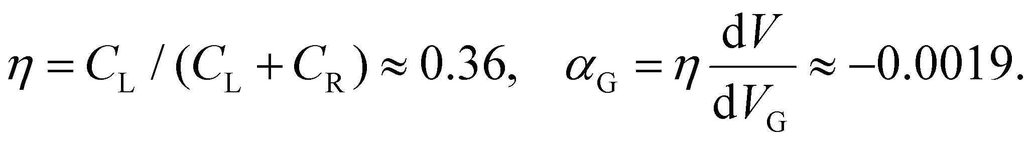
Fig. 6 is the stability diagram showing differential conductance in units of G0 as a function of V and VG at high bias and gate voltages. In this figure, we marked by the dashed lines with labels αi, βi, δi and γ the boundaries of the current triangle and steps of the tunnel current. Unlike in Fig. 5, the main current triangle in this figure defined by the lines βi and γ is strongly jagged (lines αi and δi). Also, the slope of lines βi is markedly different from the slope of line γ. The slope of lines αi is also very different from the slope of lines βi. This indicates that the jumps and shifts on the main current triangle originate from the electron switching in an adjacent, closely located and capacitively coupled arsenic dopant. One can come to such a conclusion because in the case of a single dopant charge trap located nearby, the current stability diagram shifts and additional current triangles appear,35 and the dashed lines αi and lines βi are very close to be parallel. This suggests similar capacitance parameters for this single dopant charge trap. Also this charge trap may give a small contribution to the overall tunnel current.
 | ||
| Fig. 6 Stability diagram measured at high V and VG. Current steps marked by αi and δj are due to charge trap switching nearby. The same slope of αi lines indicates that most likely they are caused by one dopant. δj lines also have the same slope, which is an indication that they are caused by a different single dopant. | ||
The left side of the current triangle bound by the γ line does not have any strong kinks, which indicates that this side corresponds to the lowest single-particle level and there are no single-particle energy levels in the surrounding dopants with a lower energy.
Using the values of  and
and 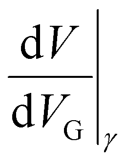 , we estimated again the bias division factor for this current triangle to be η ≈ 0.35, which is very close to η ≈ 0.36 (see eqn (3)) obtained from Fig. 5.
In the upper part of the stability diagram, between lines γ, β2 and β3, slightly jagged lines of the current maxima are seen, which correspond to the discrete single-particle levels similar to those seen in Fig. 5. The slopes of lines α2 and δ3 corresponding to the conductance jumps in the stability diagram of Fig. 6 are 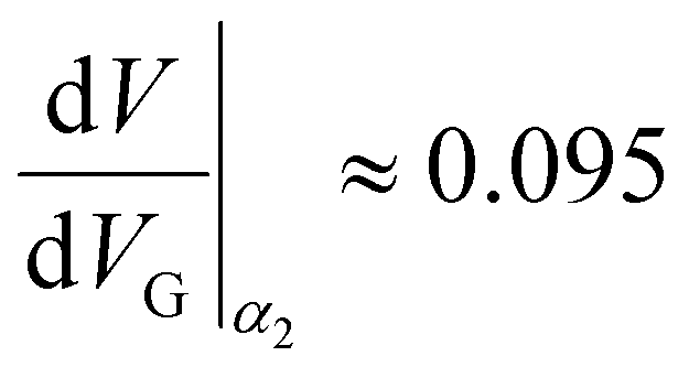 and
and 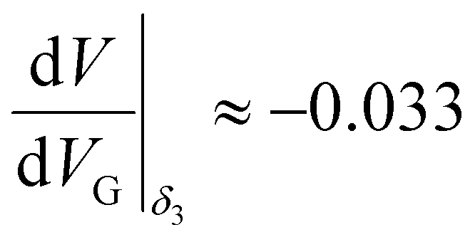 , which give αG and η equal to αG = 0.024 and η ≈ 0.74. The strong asymmetry indicates that the trap affecting the current triangle and leading to its jagged shape is in the vicinity of the dopant, but may be located closer to one of the leads.
Using the estimate for αG(3), we deduce the location of the current triangle peaks at V = 0 in energy units as EΔN=−1 ≈ −4.7 meV for the current triangle in Fig. 5 and EΔN=−3 ≈ −69.7 meV in Fig. 6. Using the values of ΔEαβ and ΔEβγ, we obtain the spacing between the single-particle energy levels corresponding to different dopant electron orbitals equal to ΔEαγ ≈ 1.97 meV. Taking into account that the number of electrons in these diamonds differs by two, we finally obtain for the charging energy 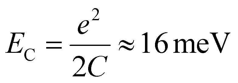 and C ≈ 5 × 10⁻¹⁸ F, which gives the average radius of the upper atomic shell of the dopant to be equal to R = 3.9 nm, which qualitatively agrees with the Bohr radius reported in ref. 36.
4. Conclusions
In conclusion, we have fabricated a single-atom single-electron transistor using SOI technology. The device was patterned in the top Si layer, which had a suitable depth profile for As dopants. The fabrication was based on a simple single-layer processing involving conventional lithographic techniques, and followed by controllable etching steps and tests of the device characteristics. This resulted in the planar single-electron transistor whose island is an implanted individual dopant center tunnel coupled to the source and drain electrodes formed by other dopants. The device was capable of sustaining the gate voltage of up to 80 V, which is the evidence for the high quality of the fabrication process. By using a simple model based on the single-electron picture of charge transport that accounts for the discrete energy levels, we obtained the key parameters of the device. The jumps in the measured stability diagram that become more pronounced at higher VG are attributed to charging and discharging of the adjacent dopants. Apparently, future applications of single-atom devices should be based on controlling the dopant's lower energy quantum states corresponding to lower VG.It is worth emphasising the key advantages of our single-atom transistor design and fabrication process in comparison with those reported in earlier studies. First, the whole process is simple and CMOS-compatible, based on commercially available SOI wafers. Second, the transistor structure is patterned in a single layer and does not require a precise alignment of the device layers. We believe this method is more convenient and accessible to those who do not have advanced electron-beam writers with precise alignment capabilities. Third, our method also allows fine trimming of the device after patterning, using short sequential etches, with a possibility to test the device transport characteristics after each etching step. Several etching steps eventually produce a device with a single dopant localized in the nanowire. Apparently, such a trimming became possible by the creation of a nonuniform dopant concentration profile in the top Si layer, before and after annealing, which allows precise control of the number of dopant atoms in the nanowire by means of etching. This trimming cannot be applied to a device in which the nanowire is covered by the gate. Fourth, the fact that our structure does not have an overlap gate has an additional advantage because in this case no interfacial layers with uncontrollable charge traps are created. The two interfaces existing in the structure with an overlap gate produce random potentials that affect the device performance and make the fabrication process less reproducible. Finally, the open device architecture allows not only post-fabrication treatment such as additional etching of the nanowire, but also implantation of extra dopants by means of a focused ion gun. The transistor with an open nanowire can be used for sensing applications, which is a long-term goal of our work. The high gate voltage used in the experiment can be reduced to about 10 V by bringing the gate closer to the nanowire, which is doable with the existing fabrication capabilities, so it will not be an issue in the optimized devices. Such open architecture demonstrated in our work allows putting a top gate after the device characterization, which will allow comparison of the device performance with side and top gates used.
Single-dopant device performance can be improved by using deep donors instead of shallow donors traditionally used in semiconductor industry. This will reduce the localization region of electrons and increase the charging energy, which should lead to a higher device operation temperature. Apparently, deeper donors will set more stringent requirements to the device fabrication. If the dopant's binding energy is X times greater than the arsenic binding energy, then, using a simple model of the rectangular tunnel barrier, one can estimate that the inter-dopant distance should be reduced by 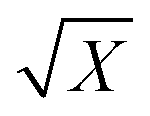 and that the dopant concentration should be increased by X3/2, in order to have the same device performance for the same layout. For example, for a binding energy of 216 meV, i.e., four times greater than the binding energy of As atoms in bulk Si, a concentration of ∼5 × 1018 cm−3 will be required. This corresponds to an average inter-dopant distance of ∼6 nm, which is within easy reach for the existing nanofabrication methods. A further improvement may be made by using a semiconductor host with a larger bandgap compared to that of Si, which should reduce the effect of thermal fluctuations and suppress intrinsic conductance. The problem of random dopant location can be addressed by using the recently developed techniques of deterministic ion implantation. An alternative way of building solitary-dopant structures could be the use of crystals with a large lattice cell containing atoms that have the properties of dopants and therefore may be suitable for constructing single-atom devices.
Author contributions
V. V. S. devised the experiment and together with V. A. K. coordinated the research efforts. D. E. P. and S. V. A. designed and fabricated the device. S. V. A. and V. A. K. performed measurements. V. V. S. and Yu. A. P. analysed the measured data and co-wrote the manuscript. All authors commented on the manuscript.Acknowledgements
We thank E. Samsonov and S. Simakin for useful discussions and acknowledge useful comments from R. George and A. S. Trifonov. Sample fabrication and characterization and analysis of the experimental data were conducted by the MSU team. The MSU team was supported by the Russian Science Foundation (Grant 16-12-00072). Yu. A. P. was supported by EPSRC (Grant EP/K01675X/1) and the Royal Society (Grant WM110105). Data and materials availability: all data used in this paper are available at http://cryolab.phys.msu.ru/images/supplementary/10.1039-C6NR07258E.zip, including descriptions of the data sets.References
- P. Gargini, ITRS past, present and future (2015) [Online], http://www.itrs2.net/itrs-reports.html (accessed: Aug 27, 2016).
- P. M. Koenraad and M. E. Flatté, Nat. Mater., 2011, 10, 91–100 CrossRef CAS PubMed.
- F. A. Zwanenburg, A. S. Dzurak, A. Morello, M. Y. Simmons, L. C. L. Hollenberg, G. Klimeck, S. Rogge, S. N. Coppersmith and M. A. Eriksson, Rev. Mod. Phys., 2013, 85, 961–1019 CrossRef CAS.
- B. E. Kane, Nature, 1998, 393, 133–137 CrossRef CAS.
- J. J. Pla, K. Y. Tan, J. P. Dehollain, W. H. Lim, J. J. Morton, D. N. Jamieson, A. S. Dzurak and A. Morello, Nature, 2012, 489, 541–545 CrossRef CAS PubMed.
- M. Fuechsle, J. A. Miwa, S. Mahapatra, H. Ryu, S. Lee, O. Warschkow, L. C. Hollenberg, G. Klimeck and M. Y. Simmons, Nat. Nanotechnol., 2012, 7, 242–246 CrossRef CAS PubMed.
- M. Veldhorst, C. H. Yang, J. C. C. Hwang, W. Huang, J. P. Dehollain, J. T. Muhonen, S. Simmons, A. Laucht, F. E. Hudson, K. M. Itoh, A. Morello and A. S. Dzurak, Nature, 2015, 526, 410–414 CrossRef CAS PubMed.
- J. A. Mol, J. Verduijn, R. D. Levine, F. Remacle and S. Rogge, Proc. Natl. Acad. Sci. U. S. A., 2011, 108, 13969–13972 CrossRef CAS PubMed.
- G. Yamahata, K. Nishiguchi and A. Fujiwara, Nat. Commun., 2014, 5, 1–7 Search PubMed.
- G. C. Tettamanzi, R. Wacquez and S. Rogge, New J. Phys., 2014, 16, 63036–63052 CrossRef.
- H. Sellier, G. P. Lansbergen, J. Caro, S. Rogge, N. Collaert, I. Ferain, M. Jurczak and S. Biesemans, Phys. Rev. Lett., 2006, 97, 206805–206808 CrossRef CAS PubMed.
- G. P. Lansbergen, R. Rahman, C. J. Wellard, I. Woo, J. Caro, N. Collaert, S. Biesemans, G. Klimeck, L. C. L. Hollenberg and S. Rogge, Nat. Phys., 2008, 4, 656–661 CrossRef CAS.
- M. Pierre, R. Wacquez, X. Jehl, M. Sanquer, M. Vinet and O. Cueto, Nat. Nanotechnol., 2010, 5, 133–137 CrossRef CAS PubMed.
- K. Y. Tan, K. W. Chan, M. Möttönen, A. Morello, C. Yang, J. van Donkelaar, A. Alves, J.-M. Pirkkalainen, D. N. Jamieson, R. G. Clark and A. S. Dzurak, Nano Lett., 2009, 10, 11–15 CrossRef PubMed.
- E. Prati, M. De Michielis, M. Belli, S. Cocco, M. Fanciulli, D. Kotekar-Patil, M. Ruoff, D. P. Kern, D. A. Wharam, J. Verduijn, G. C. Tettamanzi, S. Rogge, B. Roche, R. Wacquez, X. Jehl, M. Vinet and M. Sanquer, Nanotechnology, 2012, 23, 215204–215208 CrossRef PubMed.
- D. Moraru, A. Samanta, L. T. Anh, T. Mizuno, H. Mizuta and M. Tabe, Sci. Rep., 2014, 4, 1–6 Search PubMed.
- J. A. Miwa, J. A. Mol, J. Salfi, S. Rogge and M. Y. Simmons, Appl. Phys. Lett., 2013, 103, 043106-1–043106-4 Search PubMed.
- B. Voisin, J. Salfi, J. Bocquel, R. Rahman and S. Rogge, J. Phys.: Condens. Matter, 2015, 27, 154203–154209 CrossRef CAS PubMed.
- E. Prati, R. Latempa and M. Fanciulli, Phys. Rev. B: Condens. Matter, 2009, 80, 165331–165336 CrossRef.
- M. Gasseller, M. DeNinno, R. Loo, J. F. Harrison, M. Caymax, S. Rogge and S. H. Tessmer, Nano Lett., 2011, 11, 5208–5212 CrossRef CAS PubMed.
- S. J. Hile, M. G. House, E. Peretz, J. Verduijn, D. Widmann, T. Kobayashi, S. Rogge and M. Y. Simmons, Appl. Phys. Lett., 2015, 107, 093504 CrossRef.
- W. Kohn and J. M. Luttinger, Phys. Rev., 1955, 98, 915–922 CrossRef CAS.
- A. K. Ramdas and S. Rodriguez, Rep. Prog. Phys., 1981, 44, 1297–1387 CrossRef.
- D. V. Averin, A. N. Korotkov and K. K. Likharev, Phys. Rev. B: Condens. Matter, 1991, 44, 6199–6211 CrossRef.
- C. W. J. Beenakker, Phys. Rev. B: Condens. Matter, 1991, 44, 1646–1656 CrossRef.
- D. V. Averin and K. K. Likharev, in Single electronics: A correlated transfer of single electrons and Cooper pairs in systems of small tunnel junctions, ed. B. L. Altshuler, P. A. Lee and R. A. Webb, North-Holland, Amsterdam, 1991, vol. 30, pp. 173–271 Search PubMed.
- Yu. A. Pashkin, Y. Nakamura and J. S. Tsai, Appl. Phys. Lett., 2000, 76, 2256–2258 CrossRef CAS.
- A. B. Zorin, F.-J. Ahlers, J. Niemeyer, T. Weimann, H. Wolf, V. A. Krupenin and S. V. Lotkhov, Phys. Rev. B: Condens. Matter, 1996, 53, 13682–13687 CrossRef CAS.
- E. S. Soldatov, V. V. Khanin, A. S. Trifonov, D. E. Presnov, S. A. Yakovenko, G. B. Khomutov, S. P. Gubin and V. V. Kolesov, JETP Lett., 1996, 64, 556–560 CrossRef.
- V. A. Krupenin, D. E. Presnov, A. B. Zorin and J. Niemeyer, Physica B, 2000, 284–288(Part 2), 1800–1801 CrossRef CAS.
- L.-J. Wang, G. Cao, T. Tu, H.-O. Li, C. Zhou, X.-J. Hao, Z. Su, G.-C. Guo, H.-W. Jiang and G.-P. Guo, Appl. Phys. Lett., 2010, 97, 262113 CrossRef.
- W. Lu, Z. Ji, L. Pfeiffer, K. W. West and A. J. Rimberg, Nature, 2003, 423, 422–425 CrossRef CAS PubMed.
- Y. S. Gerasimov, V. V. Shorokhov and O. V. Snigirev, J. Supercond. Novel Magn., 2015, 28, 781–786 CrossRef CAS.
- S. M. Sze and K. K. Ng, Physics of semiconductor devices, John Wiley & Sons, Hoboken, New Jersey, 2006 Search PubMed.
- C. C. Escott, F. A. Zwanenburg and A. Morello, Nanotechnology, 2010, 21, 274018–274029 CrossRef CAS PubMed.
- J. Salfi, J. A. Mol, R. Rahman, G. Klimeck, M. Y. Simmons, L. C. L. Hollenberg and S. Rogge, Nat. Mater., 2014, 13, 605–610 CrossRef CAS PubMed.
| This journal is © The Royal Society of Chemistry 2017 |