
 Open Access Article
 This Open Access Article is licensed under a Creative Commons Attribution-Non Commercial 3.0 Unported Licence
Two-dimensional hexagonal CrN with promising magnetic and optical properties: A theoretical prediction†
Artem V.
Kuklin
 ab,
Alexander A.
Kuzubov
*ac,
Evgenia A.
Kovaleva
a,
Natalya S.
Mikhaleva
a,
Felix N.
Tomilin
ac,
Hyosun
Lee
b and
Pavel V.
Avramov
b
ab,
Alexander A.
Kuzubov
*ac,
Evgenia A.
Kovaleva
a,
Natalya S.
Mikhaleva
a,
Felix N.
Tomilin
ac,
Hyosun
Lee
b and
Pavel V.
Avramov
b
aSiberian Federal University, 79 Svobodny pr., Krasnoyarsk 660041, Russia. E-mail: alexxkuzubov@gmail.com
bDepartment of Chemistry, Kyungpook National University, 80 Daehakro, Bukgu, Daegu 41566, Republic of Korea
cL.V. Kirensky Institute of Physics, 50/38 Akademgorodok, Krasnoyarsk 660036, Russia
First published on 24th November 2016
Abstract
Half-metallic ferromagnetic materials with planar forms are promising for spintronics applications. A wide range of 2D lattices like graphene, h-BN, transition metal dichalcogenides, etc. are non-magnetic or weakly magnetic. Using first principles calculations, the existence of graphene-like hexagonal chromium nitride (h-CrN) with an almost flat atomically thin structure is predicted. We find that freestanding h-CrN has a 100% spin-polarized half-metallic nature with possible ferromagnetic ordering and a high rate of optical transparency. As a possible method for stabilization and synthesis, deposition of h-CrN on 2D MoSe2 or on MoS2 is proposed. The formation of composites retains the half-metallic properties and leads to the reduction of spin-down band gaps to 1.43 and 1.71 eV for energetically favorable h-CrN/MoSe2 and h-CrN/MoS2 configurations, respectively. Calculation of the dielectric functions of h-CrN, h-CrN/MoSe2 and h-CrN/MoS2 exhibit the high transparency of all three low-dimensional nanomaterials. The honeycomb CrN may be considered as a promising fundamental 2D material for a variety of potential applications of critical importance.
Introduction
Since the discovery of graphene, two-dimensional (2D) materials have attracted much attention due to their unique physical properties, which are very different from their bulk crystal analogs. For example, graphene – one atomic thick hexagonal layer of carbon – displays excellent thermal and electronic conductivity and reveals a unique Dirac cone in its electronic structure.1,2 In recent years many novel materials that were originally considered to exist only in the framework of theory have been synthesized. They include graphene analogues such as silicene,3,4 germanene,5 phosphorene,6 and even un-layered stanene7 and one-atom-thick boron (borophene).8During the last decade, researchers have discovered a number of different methods for the synthesis and manipulation of low-dimensional materials9 providing new two-dimensional (2D) structures to be obtained and allowing their properties to be managed through the creation of defects, modification by adatoms and integration into composites for a wide range of applications. Nanoelectronics, and in particular spintronics, are probably the most important applications of two-dimensional materials.
In the last few years, two-dimensional magnetism has attracted much attention due to the possibility of the formation of magnetic and spintronic devices using two-dimensional layers.10–12 It was recently reported that oxidized few-layer black phosphorous nanomeshes have a three-order-larger edge ferromagnetism than of graphene nanomeshes.13 However, most 2D lattices like graphene, h-BN, transition metal dichalcogenides, etc. are non-magnetic or weakly magnetic. For this reason, various ferromagnetic substrates have been used for spin injection to induce spin polarization of low-dimensional non-magnetic fragments for spin-related applications.14–16 Thin films of transition metal nitrides (TMNs) may provide one more possibility to obtain low-dimensional materials with unique spin-related properties because unpaired d-electrons are responsible for the formation of spin-ordered surface electronic states. Chromium nitride is a typical example of the TMNs family. Its bulk phase has a simple NaCl-type structure with Fm![[3 with combining macron]](https://www.rsc.org/images/entities/char_0033_0304.gif) m symmetry (paramagnetic under normal conditions) and an orthogonal phase with Pnma symmetry (antiferromagnetic).17,18 Miao and Lambrecht have discovered that the cubic phase is energetically more stable.19 It undergoes the first-order phase transition from the paramagnetic to the antiferromagnetic state with layered ordering of the magnetic moments when the temperature drops below 273 K.20–22 This means that every individual layer is a ferromagnet. Therefore, ferromagnetic ordering can be expected in 2D lattices of CrN. The substrates based on MgO, Pt or Al2O3 are generally used to obtain TMNs films.23–26 CrN thin films possess a different Néel temperature and have a slight distortion in the (001) orientation, whereas the structural distortion of the CrN (111) film is not observed.23
m symmetry (paramagnetic under normal conditions) and an orthogonal phase with Pnma symmetry (antiferromagnetic).17,18 Miao and Lambrecht have discovered that the cubic phase is energetically more stable.19 It undergoes the first-order phase transition from the paramagnetic to the antiferromagnetic state with layered ordering of the magnetic moments when the temperature drops below 273 K.20–22 This means that every individual layer is a ferromagnet. Therefore, ferromagnetic ordering can be expected in 2D lattices of CrN. The substrates based on MgO, Pt or Al2O3 are generally used to obtain TMNs films.23–26 CrN thin films possess a different Néel temperature and have a slight distortion in the (001) orientation, whereas the structural distortion of the CrN (111) film is not observed.23
Recently, monolayers of TM carbides and nitrides are actively investigated due to their potential wide application in lithium-ion batteries,27–29 electrocatalysts of hydrogen decomposition30 and nanoelectronics.31–37 Practice preparation of two-dimensional titanium carbides with OH-terminated surface demonstrated that some transition metal carbides (including mixed carbides) can also be synthesized by dipping into hydrogen fluoride acid followed by sonication.38 Subsequently two-dimensional vanadium (V2C) and niobium (Nb2C) carbides were synthesized.39 The structures of TM nitrides in most cases are similar to TM carbides due to the similar bonding type.40 Using electronic structure calculations, it was found that the one-atom-thick CrN (100) layer demonstrates spontaneous half-metallic ferromagnetism.34 The magnetic properties of the VN (111) monolayer and its composite with MgO (111) were studied using a DFT approach and DOS analysis.36 It was shown that the VN monolayer is spin-polarized and retains its properties after contact with the MgO substrate. In ref. 41, the slab thicknesses for spontaneous conversion from cubic to layered graphitic structures were determined for a number of crystalline lattices. The layered honeycomb structures are more favorable than the cubic ones for ultrathin films, including diamond, boron nitride, silicon carbide, boron phosphide and rock salt. Recently photocatalytic and piezoelectric properties with spontaneous polarization were demonstrated in the tetragonal and hexagonal forms of the NbN rocksalt structure.42 Monolayers of some transition-metal carbides MC (M = Zr, Hf) demonstrate a quantum spin Hall effect at the nanoscale.43 A short literature survey of both experimental and theoretical publications reveals a very promising possibility to develop honeycomb TMN monolayers with unique electronic and magnetic properties that provide a new perspective for spintronic applications.
In this work, the results of density functional theory (DFT+U) with consideration of weak dispersion interactions indicate directly the possibility to create a 2D chromium nitride monolayer of (111) crystallographic orientation being a 100% spin-polarized half-metallic material with high degree of optical transparency. The electronic structure calculations reveal the good match of the h-CrN crystalline lattice with 2D MoS2 and MoSe2 substrates, which opens a unique way for experimental synthesis and stabilization of 2D CrN. The results can be used for the prediction of new stable 2D polymorphs of TMNs and discovering new properties at the nanoscale.
Computational methods
All atomic and electronic structure calculations were performed using density functional theory (DFT)44,45 in the generalized gradient approximation with the Hubbard correction (GGA+U),46,47 as implemented in the Vienna Ab initio Simulation Package (VASP).48,49 The projector augmented wave (PAW)50 method and Perdew–Burke–Ernzerhof (PBE)51 exchange functional were employed. The parameter U* = U − J equal to 3 eV was chosen based on the previous studies of chromium nitride to take into account strong electron correlations.34,52 D3 Grimme correction of weak dispersion interactions53 and the Periodic Boundary Conditions (PBC) approach were used to perform electronic structure calculations of all 2D structures. To evaluate the relevance of these results, the long-corrected hybrid functional proposed by Heyd, Scuseria, and Ernzerhof (HSE06) was employed.54 The plane-wave energy cutoff was set to 500 eV. A vacuum region of 15 Å was set to avoid artificial interaction between neighboring images. The reciprocal space in the Brillouin zone was sampled using the Monkhorst–Pack scheme55 with 15 × 15 × 1 and 21 × 21 × 1 k-points for the monolayer and composites, respectively. The convergence tolerances for the force and electronic minimizations were 0.001 eV Å−1 and 10−6 eV, respectively. The phonon frequency calculations were carried out in a supercell (4 × 4 × 1) using the density functional perturbation theory (DFPT)56 and the PHONOPY code.57Results and discussion
To design the initial structural model of the two-dimensional one-atom thick CrN (111) film, an equilibrium geometry of the rocksalt-structured unit cell of CrN was optimized using the electronic structure calculations (see ESI†). Fig. 1 illustrates the schematic representation of the hexagonal 2D CrN (h-CrN) formation and its atomic structure. The unit is simple in structure and can be described as a monolayer of respective surface. The energy minimization of the corrugated (111)-oriented CrN monolayer resulted in the formation of an almost flat hexagonal sheet with minor buckling due to the reduction of a surface dipole moment. The value of buckling is ±0.071 Å (from the perfect plane) along the vacuum direction for both Cr and N atoms. The optimized h-CrN unit cell contains one chromium and one nitrogen atom with a Cr–N bond length equal to 1.884 Å, which is noticeably shorter than in the bulk (2.11 Å). Formation of h-CrN leads to the elongation of the translation vector from 2.989 Å of the exfoliated CrN (111) monolayer up to 3.258 Å of the hexagonal 2D structure. The CrN monolayer of the (110) surface also considered. During atomic force relaxations one transforms into a CrN (100) monolayer, which is discussed in ref. 33. To check the possibility of global minimum finding, we created a perfectly flat structure of CrN (111) which is an analog of graphene or h-BN. It was found that the fully relaxed structure of the flat CrN sheet is 0.01 eV higher in energy.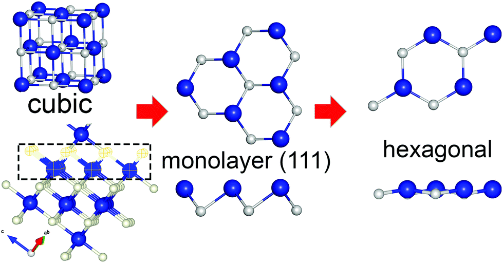 | ||
| Fig. 1 Schematic representation of h-CrN formation. Blue and grey balls correspond to Cr and N atoms, respectively. | ||
The stability of low-dimensional (1D and 2D) systems has been of key interest since the foundation of quantum and statistical mechanics.58,59 The dynamic stability of the h-CrN sheet is confirmed from the phonon frequency calculations. The calculated phonon dispersion (Fig. S1†) contains a very small imaginary acoustic frequency of 0.25 cm−1, which could be caused by phonon–magnetic coupling or strong electron correlations. Such a small value can be ignored and thus the structure can be considered as dynamically stable.60,61 Similar to the phonon frequency of graphene,62 there are three distinct acoustic modes in the phonon spectra of h-CrN, which are caused by the acoustic summation rule insufficiency. In the lattice dynamics calculations based on DFPT there is a persistent problem of non-vanishing frequencies of acoustic modes.63
Sometimes, due to the breakdown of translational symmetry for low-dimensional materials with non-equivalent sublattices, phonon calculations in periodic boundary conditions cannot be used to prove whether or not a low-dimensional crystalline lattice is a local or global minimum.64 The force constants also can be affected by phonon–magnetic coupling or strong electron correlations and soft modes may take place in magnetic and/or correlated low-dimensional systems.65,66 The newly proposed h-CrN is an example of a strongly correlated low-dimensional magnetic material with non-equivalent sublattices. Since the phonon dispersion calculations in periodic boundary conditions may not provide the final proof of h-CrN structural stability due to the presence of nonequivalent sublattices, strong correlation effects and phonon–magnetic coupling, the electronic structure calculations of extended finite nanocluster consisted of 48 atoms performed at the Γ-point (1 × 1 × 1 k-point mesh). To avoid artificial interactions between the cluster images, the vacuum interval of 20.8 Å and 9.6 Å along the perpendicular and planar directions were used. As the result of force minimization, the nanocluster becomes flat and retains in general its original crystalline lattice (see Fig. S2†) with small distortions at the edge atoms due to the edge effects. Therefore, no uncompensated mechanical stress takes place in the nanocluster and h-CrN can be considered as stable.
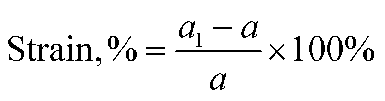
The structural stability under strain is very important for h-CrN synthesis and further applications. The h-CrN sheet is investigated by applying an equi-biaxial tensile strain (Fig. S3†) in accordance with formula (1) to estimate the mechanical stability and properties under strain.
 | (1) |
Fig. S3† shows that maximum stress occurs at 16%. Therefore, the elastic limit of the h-CrN sheet is at 0.16 strain with a maximum stress of 6.51 GPa. The supercell approach using 3 × 3 unit cells gives perfectly the same results in terms of energy and a very close result in terms of stress (Δ = 0.01 MPa). Therefore, no extra periodicity is found for the h-CrN nanosheet.
To evaluate the magnitude of exchange interactions and to find whether the ferromagnetic (FM) state is energetically favorable, the total energy spin-polarized calculations of ferromagnetic and antiferromagnetic (AFM) states of 2D h-CrN were performed using the 2 × 2 supercell. At the PBE level of theory, the ferromagnetic state is 0.715 eV lower in energy than the AFM configuration (Fig. S4†). Fig. 2(a) shows the spin density distribution of the FM configuration. Most of the spin-up density is localized on Cr2+ ions with a small portion of minority spin density localized on the nitrogen ions. The Bader analysis67 revealed an electron charge transfer of 1.52e from the transition metal to nitrogen. It is found that the charge density (Fig. 2(b)) is mainly distributed over N atoms and, in particularly, along three Cr–N bonds making in-plane orbitals responsible for the bond formation. To understand the bonding characteristics, the electron localization function (ELF)68,69 is calculated and plotted in Fig. 2(c). The ELF map is presented in values between 0.0 and 1.0. The value of 1.0 corresponds to the total of localized electrons. The electrons are localized at N atoms in the plane of the sheet, indicating that the atomic orbitals of nitrogen are characterized by sp2 hybridization. The electron density responsible for the formation of bonds is shifted towards nitrogen atoms. The N pz-orbitals correspond to the green part of ELF, revealing delocalized features. The blue distribution localized around Cr atoms indicates the electron deficiency of Cr atoms, which is in good agreement with the Bader charge analysis.
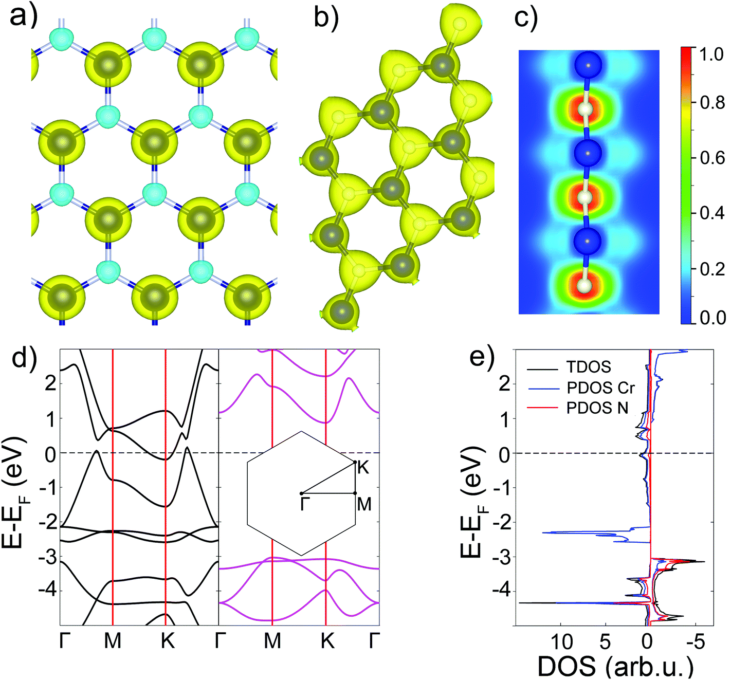 | ||
| Fig. 2 The electronic structure of h-CrN. (a) Isosurface (0.04 e Å−3) of spatial spin density distribution. The blue and green spheres correspond to majority and minority spin density, respectively. (b) Isosurface (0.1 e Å−3) of the total electronic charge density. (c) ELF map renormalized to values between 0.0 and 1.0. (d) Spin-separated band structures. Spin-up and spin-down are presented in black and pink, respectively. (e) Total and partial densities of states. TDOS, Cr PDOS and N PDOS are in black, blue and red, respectively. | ||
At the PBE level of theory, the total and partial densities of states and spin-separated band structure of h-CrN are presented in Fig. 2(d) and (e). The top spin-up valence band touches the Fermi level in the Γ–M and K–Γ intervals and the bottom of the h-CrN conductivity band crosses the Fermi level in the vicinity of the K-point. The minimum of the conductivity band is localized exactly at the K-point of the Brillouin zone with an energy of −0.2 eV. Partial filling of the spin-up conduction band provides a non-zero density of states at the Fermi level which, in combination with the spin-down band gap of 3.9 eV width, results in the 100% spin-polarized half-metallic properties of h-CrN.
Spin polarization at the Fermi level is calculated as:
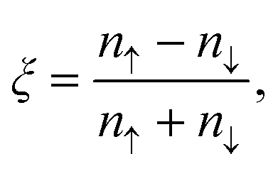 | (2) |
The HSE06 hybrid functional is used to compare the result with a higher level of theory and evaluate corrections to the spin-down band gap, which is important in optical properties evidence. In 2D systems the results of HSE06 bandgaps sometimes can be compared to the quasi-particle GW bandgaps due to the cancelling of the neglecting excitons effect.70,71 The results of HSE06 calculations demonstrate perfectly the same band gap of spin-down (3.9 eV). Bader analysis based on both PBE and HSE06 spin densities, revealing the same 3μB total magnetic moment on the Cr2+ ions, which is comparable with experimental data (3.17μB (ref. 21)) for crystalline CrN.
Cr d-, Cr p-, Cr s-, N p-, N s-orbital-projected atomic densities of states and spatial distributions of spin density in certain energy regions of the h-CrN sheet are presented in Fig. 3(a) and (b), respectively. The distribution of peaks exhibits separation of the nitrogen valence orbitals into two groups: N spxpy (a set of peaks in the [−5.73: −3.60] and [−4.85: −3.00] eV energy regions for spin-up and spin-down states, respectively); and N pz (a single peak localized in the [−4.44: −4.31] and [−3.36: −3.07] eV energy regions for spin-up and spin-down channels, respectively). Such separation of the peaks suggests sp2 hybridization of nitrogen ions. At the same time, partial peaks of Cr s, dxy and dx2−y2 states are localized in the same energy range as N s, px and py hybrid orbitals and demonstrate the exact same electronic resonance, revealing a strong overlap between them and the formation of sigma bonds lying in the h-CrN plane. Since the intensity of Cr p PDOSes is very low (in Fig. 3(a) all Cr p PDOSes are multiplied by 5 or 10), the involvement of p-orbitals in bond formation and therefore hybridization processes is minor. Spatial distribution of electronic density (Fig. 3(b)) in the range [−5.73: −5.55] eV unambiguously demonstrates the formation of σ-type Cr–N bonds caused by overlap of Cr sd2 and N sp2 hybrid orbitals.
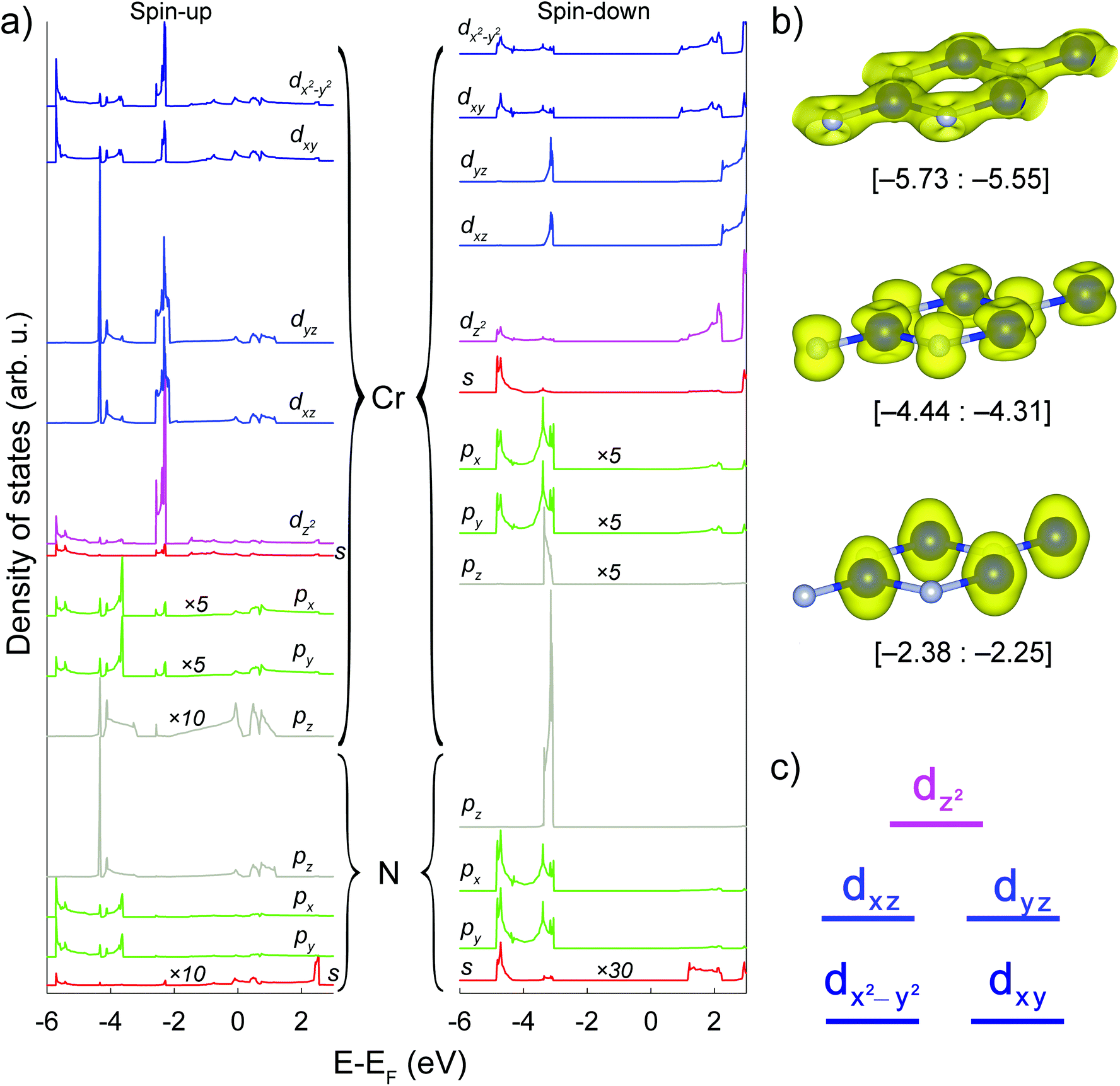 | ||
| Fig. 3 (a) Orbital-projected atomic densities of states of the h-CrN sheet. From top to bottom in braces: Cr and N orbitals, respectively. Spin-up and spin-down channels are from left to right. The densities of Cr p and N s-orbitals are multiplied by appropriate values 5, 10 or 30, respectively. The Femi level is set to zero. (b) Spatial charge distribution in [−5.73; −5.55], [−4.44; −4.31], [−2.38; −2.25] eV energy regions. (c) Qualitative Cr d-orbital diagram of h-CrN. | ||
Cr dxz and dyz-orbitals form another group of peaks distributed in the energy range of [−4.44: −4.31] eV (Fig. 3(a)) overlapping with pz-orbitals in the same energy region, resulting in p–d overlap with the formation of π-dative bonds delocalized out-of-the-plane of Cr3N3 hexagons (Fig. 3(b)). The energy region of [−2.38: −2.25] eV (Fig. 3(b)) is characterized by chromium non-binding electronic levels where the states are localized only on the Cr ions keeping N ions naked. The electronic states are constituted by all types of Cr d-orbitals, with the main contribution from the Cr dz2-orbital.
The Cr d-orbital diagram of h-CrN is presented in Fig. 3(c). The non-degenerate non-bonding Cr dz2-orbital has the highest energy and is localized on the top of valence band (energy range [−2.38: −2.25] eV). The next in energy ([−4.44: −4.31] eV) are the double-degenerate Cr dxz and Cr dyz orbitals which overlap with N pz states and form bonding π-dative orbitals localized above and below the sheet. The lowest in energy ([−5.73; −5.55] eV) doubly degenerate Cr dxy and Cr dx2−y2 states hybridize with Cr s-orbitals forming three Cr sd2 hybrid states. These orbitals overlap with N sp2 hybrid states and form σ-type bonding which forms the hexagonal sheet. The Cr d-orbital diagram of h-CrN is a typical example of the crystalline orbitals of trigonal-type complexes in terms of crystal field theory.
In practice, a synthesis of thin films is performed on substrates, which in many cases may stabilize the structure as well as affect the main structural features and properties of films. Growth of the two-dimensional CrN sheet on the appropriate substrate can be provided by CVD or PVD methods. The symmetry and lattice parameters of MoSe2 and MoS2 almost perfectly match the structural parameters of h-CrN with minor differences in the lateral translation vector of about 1–2.8% (see ESI†) and can be regarded as perfect substrates for h-CrN synthesis. We propose that this is a relevant value to grow a structure. For example, graphene can be grown on different substrates like Ni, Cu, Pt etc. that have different lattice parameters.72,73 Despite the fact that the mismatch between SiC (3.073 Å) and graphene (2.46 Å) is very large, the growth of graphene on SiC has been successfully produced.74 In addition, MoSe2 and MoS2 are nonpolar materials. Their surfaces are rather chemically inert and can easily adopt 2D modification, which is extremely important for use in nanoelectronics.
Based on the equilibrium geometry of MoSe2 and MoS2 monolayers (see ESI†), the h-CrN/MoSe2 and h-CrN/MoS2 bilayered heterostructures were simulated using the 21 × 21 k-point mesh along the periodical directions. Since the lattices of dichalcogenides have a minor mismatch with h-CrN, single unit cells were adapted to DFT+U PBE calculations. Only the most probable mutual configurations of h-CrN on MoSe2(MoS2) monolayers were considered, specifically with Cr ions coordinated either atop S(Se) ions or hollow sites, and N ions were coordinated atop Mo ions or hollow sites. The least favorable configurations, with transition metal ions (Mo and Cr) located above each other, as well as N arranged over Se(S) were not considered due to having the same sign of atomic charges of the partners.
Three possible configurations of h-CrN/MoSe2 and h-CrN/MoS2 heterostructures were revealed (Fig. 4), namely: (a) Cr_[S]–N_[Mo] or Cr_[S]–N_[Mo]; (b) Cr_[Se]–N_[hex] or Cr_[S]–N_[hex]; (c) Cr_[hex]–N_[Mo]. Here the coordination partners of h-CrN atoms (either Cr or N) are presented in square brackets and the coordination pairs are separated by dashes. The symbol [hex] denotes the location of the Cr or N ions above the centers of either MoSe2 or MoS2 hexagons.
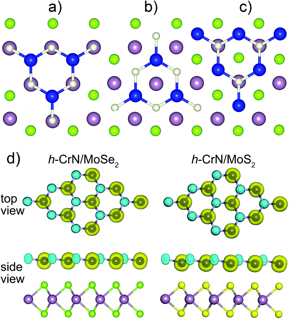 | ||
| Fig. 4 Configurations of both h-CrN/MoSe2 and h-CrN/MoS2 heterostructures. (a) Cr_[Se]–N_[Mo] and Cr_[S]–N_[Mo]. (b) Cr_[Se]–N_[hex] and Cr_[S]–N_[hex]. (c) Cr_[hex]–N_[Mo]. Blue, beige, green-yellow and light purple balls correspond to Cr, N, Se (or S) and Mo atoms, respectively. (d) Equilibrium geometries and spatial spin density distributions of h-CrN/MoSe2 and h-CrN/MoS2 composites (isosurface level is 0.03 e Å−3) in the lowest in energy configuration. The blue and green spheres correspond to the minority and majority spin densities. | ||
The cohesive energies of the composites (CrN/MoS2 and CrN/MoSe2) were evaluated according to the following formula:
| EC = ET − ET [CrN] − ET [sub] | (3) |
The lowest-energy configuration of h-CrN/MoSe2, with a cohesive energy of −0.402 eV, is Cr_[Se]–N_[Mo]. However, the Cr_[Se]–N_[hex] configuration is only 0.004 eV higher in energy (EC = −0.398 eV). The energy difference (0.053 eV) between the lowest and the highest in energy configurations (Cr_[hex]–N_[Mo], EC = −0.349 eV) is also considerably low. Since all localized configurations have only minor differences in energy, all three types of interfaces may be discovered experimentally. For the h-CrN/MoS2 heterostructure, the same Cr_[S]–N_[Mo] and Cr_[S]–N_[hex] configurations with very close cohesive energies of −0.485 eV and −0.483 eV, respectively, were localized. The energy difference (0.002 eV) between configurations is minor, so either the first or the second configuration cannot be assigned as the energetically preferable one. The cohesive energy of the third Cr_[hex]–N_[Mo] configuration is 0.114 eV higher the lowest one.
The cohesive energies and interplanar distances reveal the weak binding between the h-CrN and MoSe2(MoS2) fragments with 2.812 Å and 2.514 Å measured as Cr–Se and Cr–S distances. Short interlayer distances between h-CrN and dichalcogenides sheets can be explained by the orbital overlap, which will be presented in a later section and electrostatic interactions between positive (Cr and Mo atoms) and negative (N and Se or S) atomic charges of the fragments. The stronger binding in h-CrN/MoS2 composites is caused by the higher electronegativity and smaller atomic radius of sulfur ions. All configurations have their equilibrium geometry characterized by the location of nitrogen atoms slightly above the plane of h-CrN (Fig. 4(d)).
Despite the fact that energy difference between configurations is minor, different positions of atoms may affect the electronic structure of the whole composite. To find this out, band structures and spin-polarized DOSes of h-CrN/MoSe2 and h-CrN/MoS2 heterostructures (Fig. 5, S5 and S6†) were calculated. The interactions of h-CrN and MoSe2 lead to the spin-polarization of the MoSe2 fragment and cause the formation of small-intensity peaks near the Fermi level in the spin-up channel, whereas PDOSes of h-CrN are decreased at the Fermi level and shifted to the higher energy interval (Fig. 5(a)). The band structures at the top of the valence band and bottom of the conductivity band of Cr_[Se]–N_[Mo] and Cr_[Se]–N_[hex] configurations are changed with decreasing the density of states at the Fermi level, however, the main features of h-CrN are retained. All configurations are 100% spin polarized with a 1.43 eV spin-down band gap of the lowest-energy Cr_[Se]–N_[Mo] configuration. The third in energy configuration (Fig. S5†) demonstrates the higher spin-up density of states at the Fermi level among all three h-CrN/MoSe2 configurations. It can be concluded that the difference (in energy and electronic structure) in the final location of a nitrogen atom ([Mo] or [hex]) is negligible due to the similar distance and electrostatic interaction between the nitrogen and nearest substrate Se atoms. The minor difference between [Mo] and [hex] nitrogen configurations rises from the distance and interaction with the second substrate layer (Mo). All three h-CrN/MoSe2 configurations are similar in electronic structure and may be of interest for spin-related applications.
 | ||
| Fig. 5 Band structures (spin-up and spin-down are black and pink, respectively) and densities of states of (a) Cr_[Se]–N_[Mo] and (b) Cr_[S]–N_[Mo] configurations. DOSes of freestanding MoSe2, MoS2 and h-CrN sheets are presented in red and corresponding PDOSes are plotted in blue. Spin-up and spin-down DOS channels are demonstrated from left to right. | ||
The band structures and partial densities of state of the lowest in energy Cr_[S]–N_[Mo] and two other configurations of h-CrN/MoS2 are presented in Fig. 5(b) and S6,† respectively. The first two configurations clearly demonstrate the 100% spin-polarized half-metallic nature of h-CrN and MoS2 fragments with 1.71 eV spin-down band gaps, whereas Cr_[hex]–N_[Mo] exhibits a magnetic semiconducting nature with a narrow indirect band gap (0.17 eV) in the spin-up state and direct band gap (1.79 eV) in the spin-down state. The interactions between the fragments lead to a significant increase of the densities of state at the Fermi level in comparison with freestanding h-CrN (Fig. 2(e)), and convert MoS2 to the half-metallic state.
The Bader analysis of electronic density distribution reveals small and almost identical charge transfers of 0.07 and 0.08 electrons from h-CrN to the MoSe2 sheet for two energetically preferable configurations ([Mo] and [hex] nitrogen positions), respectively. The total charge transfers from h-CrN to the MoS2 monolayer for the [Mo] and [hex] nitrogen positions are 0.19e and 0.18e, which may be caused by stronger bonding between h-CrN and MoS2 in comparison with the h-CrN/MoSe2 composite. The higher charge transfer and lower cohesive energy are primarily caused by the higher sulfur electronegativity in comparison with selenium and the small atomic radius resulting in relatively shorter interlayer distances between MoS2 and h-CrN. The magnetic moments localized on the Cr (2.85–2.86μB) and Mo (0.10–0.11μB) ions were detected as well. The first selenium ion, which is directly bonded with Cr, has 0.027μB, whereas an almost zero magnetic moment (0.005–0.007μB for different configurations) was detected for the second Se ion, which is only bound to Mo. The Bader analysis also revealed the 2.74μB and 2.77μB magnetic moments of Cr2+ ions and 0.15μB and 0.18μB for Mo ions in the Cr_[S]–N_[Mo] and Cr_[S]–N_[hex] configurations, respectively. The sulfur ions have 0.027–0.035μB in positions directly bound to Cr and 0.015–0.017μB in positions which are only bound to Mo ions, respectively. In general, the visible reduction of Cr magnetic moments in h-CrN/MoSe2 and h-CrN/MoS2 heterostructures is caused by redistribution of the charge during the formation of weak bonds with the substrate and therefore reduction of number of unpaired electrons in the system.
The shapes of all TDOSes do not appear as a superposition of particular components (dichalcogenides and h-CrN) revealing the interaction between the monolayers. The most obvious resonance peaks are in the [−0.19: 0] eV energy interval for MoSe2 and the [−0.31: −0.21], [−1.21: −1.15], [−1.73: −1.68] eV energy intervals for MoS2. To understand the nature of the interaction between the monolayers, the spatial charge density distributions were analyzed (Fig. S7†). The peak at the Fermi level exhibits a non-binding electronic state. The formation of the h-CrN/MoSe2 composite shifts the peak to the lower energy level. This fact demonstrates weak bonding between MoSe2 and h-CrN which can be proved by the overlap in charge density distribution as well as by DOS resonance in the [−0.19: 0] eV energy interval. Partial peaks of the Cr and S states are localized in the same energy range of [−1.21: −1.15] eV and demonstrate the exact same electronic resonance, revealing a strong overlap between them. The other peaks show a more complex interaction character revealing the appearance of electron density at the Mo atoms, which can be explained as a polarization effect of the composite. It can be concluded that the interaction between the fragments leads to the orbital overlap due to the coincident peaks of h-CrN and MoSe2 or MoS2 at the Fermi level. The joint effect of electrostatic forces and orbital overlapping results in the formation of bonds between monolayers. These results indicate that the choice of a correct substrate can play a crucial role in h-CrN synthesis. In this way, both MoSe2 and MoS2 substrates keep the half-metallic properties of 2D h-CrN. The difference generally lies in the amplitude of the densities of state at the Fermi level. The MoSe2 substrate has a low electron density at the Fermi level whereas MoS2 has much higher one. It is apparent that the different S and Se electronegativity caused by the different charge transfers leads to electron density redistribution, altering the final properties of the composites.
To investigate the optical properties of h-CrN -based nanocomposites, the frequency-dependent dielectric matrix was calculated and refractive indexes (n) and extinction coefficients (k) were determined as:
 | (4) |
 | (5) |
The refractive indexes and extinction coefficients of freestanding h-CrN, h-CrN/MoSe2 and h-CrN/MoS2 composites, calculated for perpendicular light polarization are presented in Fig. 6. The intensities of h-CrN absorption and refractive spectra rapidly increase from the ultraviolet (UV) to the infrared (IR) spectral regions with a maximum in the IR region. In the UV and visible light regions one-atom-thick h-CrN exhibits high transparency and enhanced light refraction compared with graphene.75 The high transparency of h-CrN is caused by the low probabilities of averaged electronic transitions with appropriate transition energies between the valence and conduction bands.
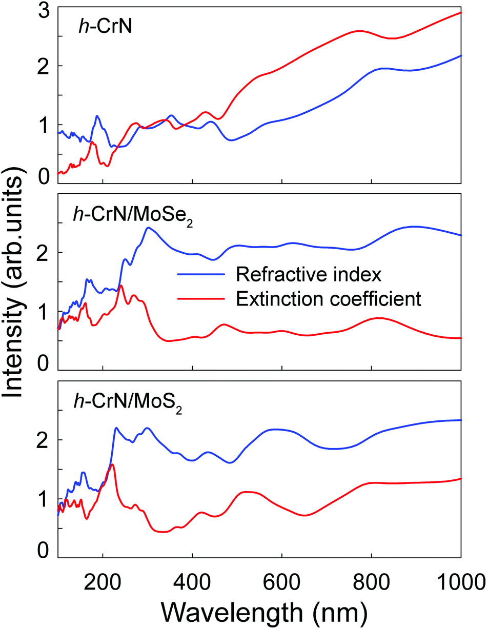 | ||
| Fig. 6 The refractive indexes n (in blue) and extinction coefficients k (in red) of freestanding h-CrN, h-CrN/MoSe2 and h-CrN/MoS2 composites (from top to bottom). | ||
The extinction coefficients of both h-CrN/MoSe2 and h-CrN/MoS2 composites become lower than those of h-CrN in the UV and visible regions. The increase of transparency of the heterostructures in comparison with freestanding h-CrN is caused by the decreased probability of averaged electronic transitions in the UV-visible light energy regions caused by the overlap of the electronic states of the h-CrN and MoSe2 or MoS2 fragments.
It is important to note that the synthesis of 2D hexagonal gallium nitride, which is similar in structure to h-CrN, was performed very recently via a migration-enhanced encapsulated growth (MEEG) technique utilizing epitaxial graphene.76 This provides new capabilities to further the synthesis of many novel 2D materials that are considered as existing only in the framework of theory for now.
Conclusions
In conclusion, a novel one-atom thick two-dimensional hexagonal CrN (h-CrN) with unique electronic properties was proposed using DFT+U electronic structure calculations. It was found that h-CrN is a 100% polarized half-metal with possible ferromagnetic ordering, which may be optimal for key spin-related applications; therefore no magnetic substrates or doping with atoms would be necessary to induce spin injection to bear spin currents, as in typical 2D materials (e.g. graphene, h-BN). The crystalline lattice of h-CrN has a 1–2.8% mismatch with the lattices of MoSe2 and MoS2, which can be used as substrates to synthesize h-CrN/MoSe2 or h-CrN/MoS2 heterostructures and finally, freestanding h-CrN. Both h-CrN/MoSe2 and h-CrN/MoS2 heterostructures retain the 100% spin-polarized half-metallic nature of h-CrN with the reduction of the h-CrN spin-down band gap from 3.9 eV to 1.43 eV and 1.71 eV, respectively. Calculations of dielectric functions of h-CrN, h-CrN/MoSe2 and h-CrN/MoS2 show the high transparency of all three low-dimensional nanomaterials.Acknowledgements
We acknowledge the Siberian Supercomputer Center (SSCC) of SB RAS, Novosibirsk; the Institute of Computational Modeling of SB RAS, Krasnoyarsk; the Joint Supercomputer Center of RAS, Moscow; and the ICC of Novosibirsk State University for providing the computing resources. This work was supported by the government contract of the Ministry of Education and Science of the Russian Federation to Siberian Federal University (Grant No. 16.1500.2014/K). P. V. A. acknowledges the Kyungpook National University Research Fund, 2014. N. S. M. acknowledges the Russian Foundation for Basic Research (RFBR 16-32-60003 mol_a_dk).References
- K. S. Novoselov, D. Jiang, F. Schedin, T. J. Booth, V. V. Khotkevich, S. V. Morozov and A. K. Geim, Proc. Natl. Acad. Sci. U. S. A., 2005, 102, 10451–10453 CrossRef CAS PubMed.
- S. Stankovich, D. A. Dikin, G. H. B. Dommett, K. M. Kohlhaas, E. J. Zimney, E. A. Stach, R. D. Piner, S. T. Nguyen and R. S. Ruoff, Nature, 2006, 442, 282–286 CrossRef CAS PubMed.
- B. Aufray, A. Kara, S. Vizzini, H. Oughaddou, C. Léandri, B. Ealet and G. Le Lay, Appl. Phys. Lett., 2010, 96, 183102 CrossRef.
- B. Lalmi, H. Oughaddou, H. Enriquez, A. Kara, S. Vizzini, B. Ealet and B. Aufray, Appl. Phys. Lett., 2010, 97, 223109 CrossRef.
- E. Bianco, S. Butler, S. Jiang, O. D. Restrepo, W. Windl and J. E. Goldberger, ACS Nano, 2013, 7, 4414–4421 CrossRef CAS PubMed.
- H. Liu, A. T. Neal, Z. Zhu, Z. Luo, X. Xu, D. Tománek and P. D. Ye, ACS Nano, 2014, 8, 4033–4041 CrossRef CAS PubMed.
- F. Zhu, W. Chen, Y. Xu, C. Gao, D. Guan, C. Liu, D. Qian, S.-C. Zhang and J. Jia, Nat. Mater., 2015, 14, 1020–1025 CrossRef CAS PubMed.
- A. J. Mannix, X.-F. Zhou, B. Kiraly, J. D. Wood, D. Alducin, B. D. Myers, X. Liu, B. L. Fisher, U. Santiago, J. R. Guest, M. J. Yacaman, A. Ponce, A. R. Oganov, M. C. Hersam and N. P. Guisinger, Science, 2015, 350, 1513–1516 CrossRef CAS PubMed.
- S. Z. Butler, S. M. Hollen, L. Cao, Y. Cui, J. A. Gupta, H. R. Gutiérrez, T. F. Heinz, S. S. Hong, J. Huang, A. F. Ismach, E. Johnston-Halperin, M. Kuno, V. V. Plashnitsa, R. D. Robinson, R. S. Ruoff, S. Salahuddin, J. Shan, L. Shi, M. G. Spencer, M. Terrones, W. Windl and J. E. Goldberger, ACS Nano, 2013, 7, 2898–2926 CrossRef CAS PubMed.
- J. Haruyama, Electronics, 2013, 2, 368–386 CrossRef CAS.
- T. Hashimoto, S. Kamikawa, D. Soriano, J. G. Pedersen, S. Roche and J. Haruyama, Appl. Phys. Lett., 2014, 105, 183111 CrossRef.
- C. Ohata, R. Tagami, Y. Nakanishi, R. Iwaki, K. Nomura and J. Haruyama, Appl. Phys. Lett., 2016, 109, 133110 CrossRef.
- Y. Nakanishi, A. Ishi, C. Ohata, D. Soriano, R. Iwaki, K. Nomura, M. Hasegawa, T. Nakamura, S. Katsumot, S. Roch and J. Haruyama, Nano Res., 2016 DOI:10.1007/s12274-016-1355-8.
- E. A. Kovaleva, A. A. Kuzubov, P. V. Avramov, A. V. Kuklin, N. S. Mikhaleva and P. O. Krasnov, Org. Electron., 2016, 37, 55–60 CrossRef CAS.
- M. V. Kamalakar, A. Dankert, J. Bergsten, T. Ive and S. P. Dash, Sci. Rep., 2014, 4, 6146 CrossRef CAS PubMed.
- A. A. Kuzubov, E. A. Kovaleva, P. Avramov, A. V. Kuklin, N. S. Mikhaleva, F. N. Tomilin, S. Sakai, S. Entani, Y. Matsumoto and H. Naramoto, J. Appl. Phys., 2014, 116, 84309 CrossRef.
- P. A. Bhobe, A. Chainani, M. Taguchi, T. Takeuchi, R. Eguchi, M. Matsunami, K. Ishizaka, Y. Takata, M. Oura, Y. Senba, H. Ohashi, Y. Nishino, M. Yabashi, K. Tamasaku, T. Ishikawa, K. Takenaka, H. Takagi and S. Shin, Phys. Rev. Lett., 2010, 104, 236404 CrossRef CAS PubMed.
- L. M. Corliss, N. Elliott and J. M. Hastings, Phys. Rev., 1960, 117, 929–935 CrossRef CAS.
- M. S. Miao and W. R. L. Lambrecht, Phys. Rev. B: Condens. Matter, 2005, 71, 214405 CrossRef.
- J. D. Browne, P. R. Liddell, R. Street and T. Mills, Phys. Status Solidi A, 1970, 1, 715–723 CrossRef CAS.
- R. M. Ibberson and R. Cywinski, Physica B: Condens. Matter, 1992, 180–181, 329–332 CrossRef CAS.
- C. R. Eddine, M. N. Sayetat, F. Felix and E. Hebd, Seances Acad. Sci., Ser. B, 1969, 269, 574–577 Search PubMed.
- C. Constantin, M. B. Haider, D. Ingram and A. R. Smith, Appl. Phys. Lett., 2004, 85, 6371 CrossRef CAS.
- A. Glaser, S. Surnev, M. G. Ramsey, P. Lazar, J. Redinger, R. Podloucky and F. P. Netzer, Surf. Sci., 2007, 601, 4817–4823 CrossRef CAS.
- P. Lazar, B. Rashkova, J. Redinger, R. Podloucky, C. Mitterer, C. Scheu and G. Dehm, Thin Solid Films, 2008, 517, 1177–1181 CrossRef CAS.
- K. Inumaru, K. Koyama, N. Imo-oka and S. Yamanaka, Phys. Rev. B: Condens. Matter, 2007, 75, 54416 CrossRef.
- E. Yang, H. Ji, J. Kim, H. Kim and Y. Jung, Phys. Chem. Chem. Phys., 2015, 17, 5000–5005 RSC.
- C. Eames and M. S. Islam, J. Am. Chem. Soc., 2014, 136, 16270–16276 CrossRef CAS PubMed.
- A. L. Ivanovskii and A. N. Enyashin, Russ. Chem. Rev., 2013, 82, 735–746 CrossRef.
- W.-F. Chen, J. T. Muckerman and E. Fujita, Chem. Commun., 2013, 49, 8896 RSC.
- Z. Zhang, X. Liu, B. I. Yakobson and W. Guo, J. Am. Chem. Soc., 2012, 134, 19326–19329 CrossRef CAS PubMed.
- R.-Q. Zhang, C.-E. Kim, B. Delley, C. Stampfl and A. Soon, Phys. Chem. Chem. Phys., 2012, 14, 2462–2467 RSC.
- Y. Bai, K. Deng and E. Kan, RSC Adv., 2015, 5, 18352–18358 RSC.
- S. Zhang, Y. Li, T. Zhao and Q. Wang, Sci. Rep., 2014, 4, 5241 CAS.
- M. Khazaei, M. Arai, T. Sasaki, C.-Y. Chung, N. S. Venkataramanan, M. Estili, Y. Sakka and Y. Kawazoe, Adv. Funct. Mater., 2013, 23, 2185–2192 CrossRef CAS.
- A. V. Kuklin, A. A. Kuzubov, N. S. Eliseeva, F. N. Tomilin, A. S. Fedorov and P. O. Krasnov, Phys. Solid State, 2014, 56, 229–234 CrossRef CAS.
- S. Zhao, W. Kang and J. Xue, Appl. Phys. Lett., 2014, 104, 133106 CrossRef.
- M. Naguib, O. Mashtalir, J. Carle, V. Presser, J. Lu, L. Hultman, Y. Gogotsi and M. W. Barsoum, ACS Nano, 2012, 6, 1322–1331 CrossRef CAS PubMed.
- M. Naguib, J. Halim, J. Lu, K. M. Cook, L. Hultman, Y. Gogotsi and M. W. Barsoum, J. Am. Chem. Soc., 2013, 135, 15966–15969 CrossRef CAS PubMed.
- J. Häglund, A. Fernández Guillermet, G. Grimvall and M. Körling, Phys. Rev. B: Condens. Matter, 1993, 48, 11685–11691 CrossRef.
- P. B. Sorokin, A. G. Kvashnin, Z. Zhu and D. Tománek, Nano Lett., 2014, 14, 7126–7130 CrossRef CAS PubMed.
- S. Anand, K. Thekkepat and U. V. Waghmare, Nano Lett., 2016, 16, 126–131 CrossRef CAS PubMed.
- L. Zhou, B. Shao, W. Shi, Y. Sun, C. Felser, B. Yan and T. Frauenheim, 2D Mater., 2016, 3, 35022 CrossRef.
- W. Kohn and L. J. Sham, Phys. Rev., 1965, 140, A1133–A1138 CrossRef.
- P. Hohenberg, Phys. Rev., 1964, 136, B864–B871 CrossRef.
- V. I. Anisimov, J. Zaanen and O. K. Andersen, Phys. Rev. B: Condens. Matter, 1991, 44, 943–954 CrossRef CAS.
- S. L. Dudarev, S. Y. Savrasov, C. J. Humphreys and A. P. Sutton, Phys. Rev. B: Condens. Matter, 1998, 57, 1505–1509 CrossRef CAS.
- G. Kresse and J. Furthmüller, Phys. Rev. B: Condens. Matter, 1996, 54, 11169–11186 CrossRef CAS.
- G. Kresse and J. Hafner, Phys. Rev. B: Condens. Matter, 1993, 47, 558–561 CrossRef CAS.
- P. E. Blöchl, Phys. Rev. B: Condens. Matter, 1994, 50, 17953–17979 CrossRef.
- J. P. Perdew, K. Burke and M. Ernzerhof, Phys. Rev. Lett., 1996, 77, 3865–3868 CrossRef CAS PubMed.
- A. Herwadkar and W. R. L. Lambrecht, Phys. Rev. B: Condens. Matter, 2009, 79, 35125 CrossRef.
- S. Grimme, J. Comput. Chem., 2006, 27, 1787–1799 CrossRef CAS PubMed.
- J. Heyd, G. E. Scuseria and M. Ernzerhof, J. Chem. Phys., 2003, 118, 8207 CrossRef CAS.
- H. J. Monkhorst and J. D. Pack, Phys. Rev. B: Solid State, 1976, 13, 5188–5192 CrossRef.
- S. Baroni, S. de Gironcoli, A. Dal Corso and P. Giannozzi, Rev. Mod. Phys., 2001, 73, 515–562 CrossRef CAS.
- A. Togo and I. Tanaka, Scr. Mater., 2015, 108, 1–5 CrossRef CAS.
- E. M. Landau and L. D. Lifshitz, Quantum Mechanics, Pergamon, Oxford, U.K., 1981 Search PubMed.
- E. M. Landau and L. D. Lifshitz, Statistical Physics Part I, Oxford, U.K., 1980 Search PubMed.
- I. Choudhuri, S. Kumar, A. Mahata, K. S. Rawat and B. Pathak, Nanoscale, 2016, 8, 14117–14126 RSC.
- J. Zhou, J. Huang, B. G. Sumpter, P. R. C. Kent, Y. Xie, H. Terrones and S. C. Smith, J. Phys. Chem. C, 2014, 118, 16236–16245 CAS.
- C. A. Marianetti and H. G. Yevick, Phys. Rev. Lett., 2010, 105, 245502 CrossRef CAS PubMed.
- A. Živković and I. Lukačević, J. Alloys Compd., 2016, 682, 839–843 CrossRef.
- P. Avramov, V. Demin, M. Luo, C. H. Choi, P. B. Sorokin, B. Yakobson and L. Chernozatonskii, J. Phys. Chem. Lett., 2015, 6, 4525–4531 CrossRef CAS PubMed.
- N. Nakanishi, A. Nagasawa and Y. Murakami, J. Phys. Colloq., 1982, 43, 4–35 CrossRef.
- A. B. Mei, O. Hellman, N. Wireklint, C. M. Schlepütz, D. G. Sangiovanni, B. Alling, A. Rockett, L. Hultman, I. Petrov and J. E. Greene, Phys. Rev. B: Condens. Matter, 2015, 91, 54101 CrossRef.
- E. Sanville, S. D. Kenny, R. Smith and G. Henkelman, J. Comput. Chem., 2007, 28, 899–908 CrossRef CAS PubMed.
- A. D. Becke and K. E. Edgecombe, J. Chem. Phys., 1990, 92, 5397 CrossRef CAS.
- A. Savin, O. Jepsen, J. Flad, O. K. Andersen, H. Preuss and H. G. von Schnering, Angew. Chem., Int. Ed. Engl., 1992, 31, 187–188 CrossRef.
- J.-H. Choi, P. Cui, H. Lan and Z. Zhang, Phys. Rev. Lett., 2015, 115, 66403 CrossRef PubMed.
- V. Tran, R. Soklaski, Y. Liang and L. Yang, Phys. Rev. B: Condens. Matter, 2014, 89, 235319 CrossRef.
- X. Li, W. Cai, L. Colombo and R. S. Ruoff, Nano Lett., 2009, 9, 4268–4272 CrossRef CAS PubMed.
- P. Sutter, J. T. Sadowski and E. Sutter, Phys. Rev. B: Condens. Matter, 2009, 80, 245411 CrossRef.
- F. Bonaccorso, A. Lombardo, T. Hasan, Z. Sun, L. Colombo and A. C. Ferrari, Mater. Today, 2012, 15, 564–589 CrossRef CAS.
- E. Ochoa-Martínez, M. Gabás, L. Barrutia, A. Pesquera, A. Centeno, S. Palanco, A. Zurutuza and C. Algora, Nanoscale, 2015, 7, 1491–1500 RSC.
- Z. Y. Al Balushi, K. Wang, R. K. Ghosh, R. A. Vilá, S. M. Eichfeld, J. D. Caldwell, X. Qin, Y.-C. Lin, P. A. DeSario, G. Stone, S. Subramanian, D. F. Paul, R. M. Wallace, S. Datta, J. M. Redwing and J. A. Robinson, Nat. Mater., 2016, 15, 1166–1171 CrossRef CAS PubMed.
Footnote |
| † Electronic supplementary information (ESI) available: The GGA DFT optimized geometry for the bulk CrN, MoSe2 and MoS2; phonon band structure; equilibrium structure of the h-CrN nanocluster; equi-biaxial strain vs. energy and vs. stress plot for h-CrN; isosurface of h-CrN AFM state; band structures and densities of states of both composites; spatial charge distribution of h-CrN, h-CrN/MoSe2, h-CrN/MoS2. See DOI: 10.1039/c6nr07790k |
| This journal is © The Royal Society of Chemistry 2017 |