
Efficient organic photovoltaic cells on a single layer graphene transparent conductive electrode using MoOx as an interfacial layer†
J. H.
Du‡
*a,
H.
Jin‡
*b,
Z. K.
Zhang
a,
D. D.
Zhang
a,
S.
Jia
a,
L. P.
Ma
a,
W. C.
Ren
a,
H. M.
Cheng
a and
P. L.
Burn
b
aShenyang National Laboratory for Materials Science, Institute of Metal Research, Chinese Academy of Sciences, 72 Wenhua Road, Shenyang 110016, P. R. China. E-mail: jhdu@imr.ac.cn
bCentre for Organic Photonics & Electronics, The University of Queensland, Brisbane, QLD 4072, Australia. E-mail: h.jin1@uq.edu.au
First published on 22nd November 2016
Abstract
The large surface roughness, low work function and high cost of transparent electrodes using multilayer graphene films can limit their application in organic photovoltaic (OPV) cells. Here, we develop single layer graphene (SLG) films as transparent anodes for OPV cells that contain light-absorbing layers comprised of the evaporable molecular organic semiconductor materials, zinc phthalocyanine (ZnPc)/fullerene (C60), as well as a molybdenum oxide (MoOx) interfacial layer. In addition to an increase in the optical transmittance, the SLG anodes had a significant decrease in surface roughness compared to two and four layer graphene (TLG and FLG) anodes fabricated by multiple transfer and stacking of SLGs. Importantly, the introduction of a MoOx interfacial layer not only reduced the energy barrier between the graphene anode and the active layer, but also decreased the resistance of the SLG by nearly ten times. The OPV cells with the structure of polyethylene terephthalate/SLG/MoOx/CuI/ZnPc/C60/bathocuproine/Al were flexible, and had a power conversion efficiency of up to 0.84%, which was only 17.6% lower than the devices with an equivalent structure but prepared on commercial indium tin oxide anodes. Furthermore, the devices with the SLG anode were 50% and 86.7% higher in efficiency than the cells with the TLG and FLG anodes. These results show the potential of SLG electrodes for flexible and wearable OPV cells as well as other organic optoelectronic devices.
Introduction
Organic photovoltaic (OPV) cells have attracted substantial scientific and commercial interest due to their light weight, compatibility with flexible substrates, suitability for roll-to-roll mass production and potentially low cost.1–3 A critical component of the OPV cell is the transparent conductive electrode (TCE), which acts as a window for light to pass into the device as well as the means of charge extraction. As such the TCE plays a critical role in device performance. To date, transparent indium tin oxide (ITO) is the most commonly used TCE in OPV cells. However, the rapid reduction of indium reserves, the highly brittle nature of ITO, and the effect of indium ion diffusion into the organic semiconductor layers indicate that alternative TCEs need to be developed if OPV technology is going to reach its potential.4–6Graphene, a single layer of sp2-hybridized carbon atoms bonded together in a hexagonal “honeycomb” lattice, has remarkable electrical conductivity, optical transmittance, mechanical flexibility, and chemical stability. These properties and the successful synthesis of large-area graphene by chemical vapor deposition (CVD) have led to growing interest in its application for OPV cells as an alternative to ITO as the TCE.7–9 However, the CVD-grown single layer graphene (SLG) has a high sheet resistance, typically ∼600–1000 Ω sq−1, with 97% transmittance, which in both cases is much higher than that of ITO (∼10 Ω sq−1 with 85% transmittance), and hence is generally thought as unsuitable for OPV applications.9 Therefore, the early demonstration of OPV cells with graphene electrodes usually used multilayer graphene films that were produced by multiple transfer and stacking of CVD-grown SLGs to reduce the sheet resistance.10–12 However, the multiple transfer and stacking processes have a number of drawbacks. First, they are time-consuming and greatly increase the production cost of graphene TCEs. Second, the light transmittance of the multilayer graphene TCEs is reduced since each additional layer absorbs ∼3% of the incident light.13 Third, multiple transfer and stacking can lead to a significant increase of the surface roughness of the graphene TCE. That is, the density and surface feature heights due to wrinkles and polymer residues such as poly(methyl methacrylate) (PMMA), which originate from the growth and transfer processing, are increased.14,15 A large surface roughness can give rise to a high leakage current, act as potential shunt pathways, and even cause electrical shorts between the graphene and the metal electrodes through the organic semiconductor layer. Furthermore, residues such as PMMA are electrical insulators and hence may inhibit charge extraction, and if in a particulate form can decrease the device uniformity.16 Thus, there is strong impetus to improve the performance of SLG films to avoid the problems of the multilayer graphene electrodes.
The introduction of an interfacial layer between the electrodes and the organic semiconductor layers has been shown to improve the power conversion efficiency (PCE) of OPV cells by optimizing the electrical contacts leading to a reduction in charge recombination at the electrodes and hence improving charge collection.17,18 Poly(3,4-ethylenedioxythiophene):poly(styrenesulfonate) (PEDOT:PSS) is the most widely used interfacial layer material for TCEs. However, the hydrophobic nature of the graphene surface makes it difficult to deposit PEDOT:PSS uniformly over its surface.14 Moreover, the work function of PEDOT:PSS (∼5.2 eV) is relatively low, and its acidic nature may cause the devices to have reliability issues.19,20 Molybdenum oxide (MoOx, 2 < x < 3) has shown promising results as an interfacial layer for graphene TCEs in optoelectronic devices.14,21,22 It can be processed by evaporation and depending on the conditions can have a work function as high as ∼6.4 eV, although it is sensitive to moisture.23 More importantly, MoOx can also act as a p-type dopant to decrease the resistance of graphene TCEs.24,25 Therefore, MoOx has potential to simultaneously enhance charge extraction and increase the electrical conductivity of graphene TCEs.
Here, we report the first use of CVD-grown SLG films as transparent anodes for OPV cells with evaporable molecular organic semiconductor light-absorbing layers, namely a bilayer structure of zinc phthalocyanine (ZnPc)/fullerene (C60). A MoOx layer was thermally deposited onto the SLG TCE to form an interfacial layer to simultaneously increase the conductivity of the graphene and reduce the energy barrier between the graphene anode and the active layer. In addition to an optical transmittance increase, the SLG anode has shown a significant decrease in surface roughness compared to two and four layer graphene (TLG and FLG) TCEs fabricated by the multiple transfer and stacking of CVD-grown SLGs. More importantly, the introduction of the MoOx interfacial layer caused the SLG anode to have a significantly reduced resistance, which is closer to that of the TLG and FLG anodes. In addition to excellent flexibility, the OPV cells with SLG anodes on plastic substrates (∼1000 Ω sq−1) had an open circuit voltage (VOC) of 0.44 V, short circuit current density (JSC) of 5.2 mA cm−2, fill factor (FF) of 0.37, and a PCE (η) of 0.84%. The PCE was only 17.6% lower than that of devices with the same organic semiconductor layers but using the more conductive ITO as the anode (15 Ω sq−1). In addition, the PCE of devices with SLG anodes was 50% and 86.7% higher than that of the devices using TLG and FLG anodes, respectively.
Experimental
Fabrication of graphene TCEs and OPV cells
Fig. 1 shows the fabrication process of the OPV cells by using graphene transparent anodes and a MoOx interfacial layer. First, an SLG film (Fig. S1†) was synthesized by CVD on a copper foil.26 It was then transferred onto a poly(ethylene terephthalate) (PET) substrate with dimensions of 2.5 × 2.5 cm2. The SLG TCE was obtained by etching away the Cu foil in an aqueous solution of FeCl3 (0.03 g mL−1) with spin-coated PMMA as a protecting layer, which was subsequently dissolved in warm acetone.27–29 TLG and FLG TCEs were obtained by transfer and stacking two and four layers of the SLG films, one by one, onto a PET substrate, respectively. Subsequently, the TCE was patterned by mechanically rubbing away the peripheral area along the two opposite sides. After patterning, the graphene anode was loaded into a high vacuum chamber to deposit two Ag contact electrodes, a 30 nm MoOx interfacial layer, followed sequentially by a 5 nm CuI buffer layer, 25 nm ZnPc and 35 nm C60 light-absorbing layers, a 10 nm bathocuproine (BCP) hole blocking layer, and an Al cathode (PET/graphene/MoOx/CuI/ZuPc/C60/BCP/Al). Each substrate contained 6 devices, and each device had a 0.2 cm2 active area defined by the cathode. For comparison, OPV cells were also fabricated on an ITO (Xin Yan Ltd) TCE on glass. Before device fabrication, the ITO on glass was sonicated sequentially in Alconox detergent, deionized water, acetone, and 2-propanol, and dried under a nitrogen gas flow.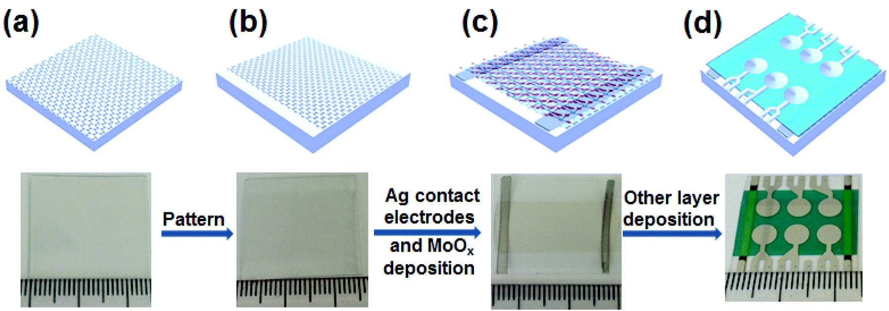 | ||
| Fig. 1 Fabrication of OPV cells comprised of an SLG anode and a MoOx interfacial layer. (a) A CVD-grown graphene film on a PET substrate formed by transfer of a graphene film grown on a Cu foil, (b) a patterned graphene TCE, (c) Ag contact electrodes with MoOx deposited on the graphene film, (d) OPV cells made by sequential deposition of a CuI buffer layer, evaporable molecular organic semiconductor light-absorbing layers, a BCP hole blocking layer and an Al cathode. | ||
Characterization
An Atomic Force Microscope (AFM, Veeco MultiMode NanoScope IIIa, tapping mode) was used to characterize the surface morphology of the MoOx film on graphene. The surface roughness of graphene on PET and ITO on glass was characterized by using a WYKO NT 1000 profiler. The sheet resistance and transmittance of the graphene and ITO TCEs were measured by using a 4-probe resistivity measurement system (RTS-9, Guangzhou, China) and a UV-vis-NIR spectrometer (Varian Cary 5000), respectively. Current–voltage characterization of the OPV cells was performed by using a Keithley 2400 source measurement unit in a four-point source-sense configuration under a N2 atmosphere in a glove box (H2O < 0.1 ppm and O2 < 0.1 ppm). An AM 1.5G solar simulator (ABET Technologies) at 100 mW cm−2 intensity was used for illumination measurements. External Quantum Efficiency (EQE) measurements (Incident Photon Conversion Efficiency – IPCE) were obtained by using a QEX7 setup from PV Measurements Inc, which was operated without white light bias and chopped and locked in the small perturbation limit.Results and discussion
We first measured the transmittance, sheet resistance and surface roughness of the SLG TCE and compared it with those of TLG, FLG and ITO TCEs. As shown in Fig. 2a, the transmittance of the SLG TCE at 550 nm wavelength was as high as 96.5%, which is higher than that of the TLG (92.7%), FLG (84.1%) and ITO (80.7%) TCEs. The presence of small islands on the surface of the SLG film leads to the transmittance being slightly lower than that of a perfect monolayer of graphene (97.7%). However, the SLG had a sheet resistance of ∼1000 Ω sq−1 (Fig. 2b), which is nearly two times higher than that of the TLG anode (∼600 Ω sq−1), four times higher than that of the FLG anode (∼260 Ω sq−1), and 70 times higher than that of the standard commercial ITO TCE on glass (15.0 Ω sq−1). Fig. 2d–f show the typical surface profiler images of the SLG, TLG and FLG films. It was found that the three graphene TCEs had no big difference in the average surface roughness (Ra), with the arithmetic average of the absolute values of the roughness profiles being about 8–12 nm, which is 3–4 times higher than that of commercial ITO on glass (∼3.3 nm, Fig. S2†). One reason for the high average roughness of the graphene anodes is that the PET substrate has a Ra of about 10 nm. However, there was a distinct difference in the maximum distance of peak to valley (where Rt is the vertical distance between the highest and the lowest points in the evaluated area) for each of the materials investigated. Rt is critical as it gives information as to whether the devices are likely to be short circuited. As shown in Fig. 2c, SLG has a similar Rt (54.3 nm) to that of commercial ITO on glass (40.1 nm), but it is much lower than that of both the TLG (264.9 nm) and FLG (349.9 nm) anodes, indicating that an increase in the number of graphene layers has a significant effect on the peak surface roughness of the graphene TCEs. It is clear that there are more red sharp peaks (indicating the highest peaks) for the FLG than the TLG anodes (Fig. 2e and f), while the SLG anode has almost no such peaks (Fig. 2d). Thus overall, with respect to transparency and surface roughness, the SLG TCE is better for devices than the multilayer graphene films, but to be used effectively the sheet resistance must be substantially reduced. | ||
| Fig. 2 (a) Transmittance, (b) sheet resistance, and (c) Rt of graphene TCEs with different numbers of layers on PET, and an ITO TCE on glass. Optical surface profiler images and the measured roughness (scale bar) of the (d) SLG, (e) TLG, and (f) FLG TCEs. | ||
The high work function transition metal oxide, MoOx, has been widely used as an interfacial layer in OPV cells to improve the hole extraction from the organic semiconductor layer.30,31 Furthermore, the large work function difference between MoOx (∼6.4 eV) and graphene (∼4.4 eV) can lead to electron transfer from graphene to MoOx at the graphene/MoOx interface, and hence p-doping of the graphene anode.25 A 30 nm thick MoOx was vacuum evaporated onto the SLG surface, which only caused a small decrease in the transmittance of the SLG TCE at 550 nm – from 96.5% to 91% (Fig. S3†), which is still higher than pristine FLG on PET and ITO on glass TCEs (Fig. 2a). The AFM image (Fig. 3a) shows that the MoOx layer is uniformly deposited onto the SLG/PET. To evaluate the effect of the MoOx interlayer on the conductivity of the SLG TCE, the electrical resistance of a SLG film with an area of 2 × 1.5 cm2 was measured between two Ag contact electrodes (Fig. 1c) before and after MoOx deposition using a multimeter in a glove box. For comparison, the electrical resistance of TLG, FLG and ITO anodes were also measured before and after MoOx deposition. It was worthy of note that the multimeter is easily taken into the glove box to measure the electrical resistance (not sheet resistance) of the graphene TCEs, and importantly the two Ag contact electrodes precisely define the measurement area and guarantee that the same area was measured before and after MoOx deposition. As shown in Fig. 3b, the deposition of MoOx dramatically decreased the electrical resistance of the SLG anode, by nearly a factor of ten, (from 4430 to 539 Ω) but only halved the resistance of the TLG anodes to 593 Ω from 1015 Ω. In the case of the FLG anodes there was little difference in the resistance (∼365 Ω in both cases). Thus the graphene–MoOx interaction has the greatest effect on the graphene TCEs with the fewest layer numbers. This would indicate that hole doping tends to occur at the MoOx/graphene interface independent of the number of graphene layers. Consequently, the use of a MoOx interlayer or similar is important when using SLG as the TCE in optoelectronic devices. In contrast, we did not observe any influence of a MoOx interfacial layer on the resistance of the ITO TCE on glass.
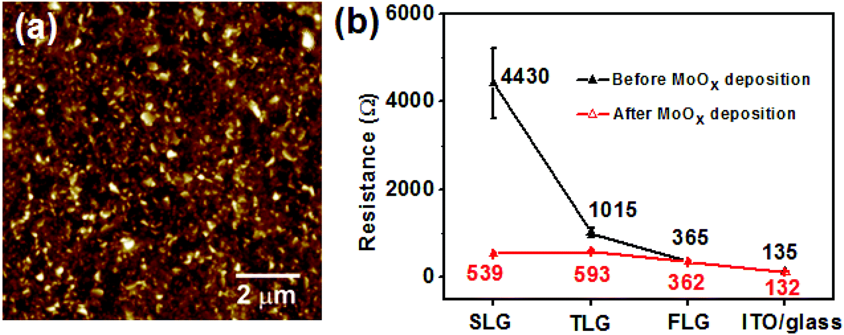 | ||
| Fig. 3 (a) AFM image of the MoOx (30 nm) film on SLG/PET, and (b) electrical resistance of graphene films with different numbers of layers on PET and ITO on glass before and after MoOx deposition. The resistance was measured between two Ag contacts on a film with a defined area of 2 × 1.5 cm2. | ||
OPV cells using the SLG anode and the MoOx interfacial layer with the structure of PET/SLG/MoOx (30 nm)/CuI (5 nm)/ZnPc (25 nm)/C60 (35 nm)/BCP (10 nm)/Al (80 nm) were prepared and compared to the identical devices made with TLG, FLG, and ITO TCEs. A schematic device structure and the corresponding energy levels are shown in Fig. 4a and b, respectively, and Fig. 4c is the picture of an OPV cell fabricated on the SLG anode. Each cell had an effective area of 0.2 cm2 and showed excellent flexibility. The CuI (5 nm) was used as a template for the growth of face-on ZnPc (as opposed to edge-on) to achieve a higher VOC.32–34 It is worth noting that a CuI layer also reduced the resistance of the SLG anode, but the effect was smaller than that measured when MoOx was used. The measured electrical resistance of the SLG anode covered with a thin CuI layer was 876 Ω, much lower than that of the pristine SLG (4430 Ω), but 1.6 times higher than that of the MoOx/SLG anode (539 Ω). More importantly, deposition of the CuI layer had no significant effect on the resistance of MoOx/graphene anodes.
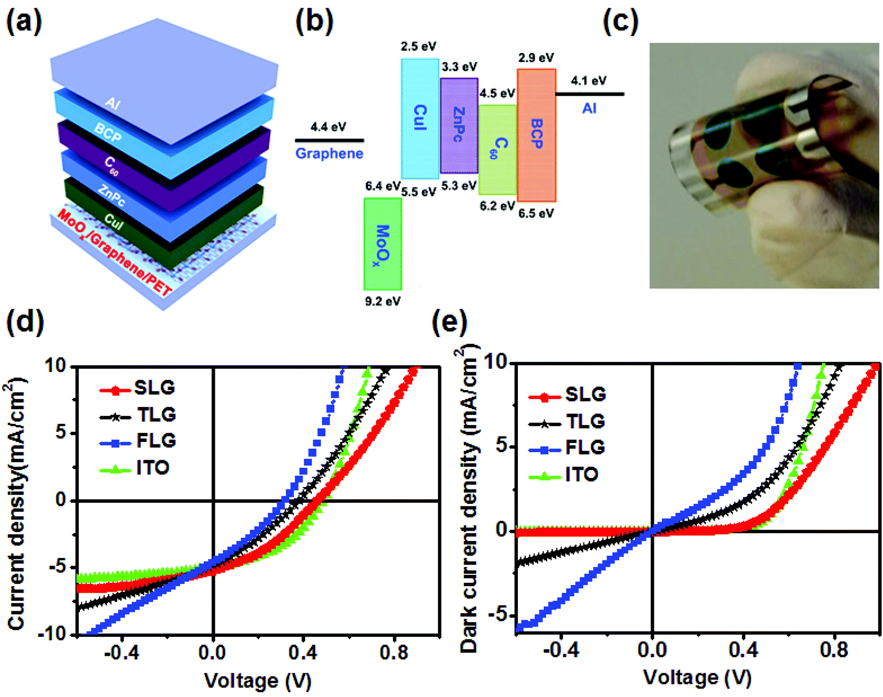 | ||
| Fig. 4 (a) Schematic of the OPV cell structure, (b) energy levels (it should be noted that, as these are measured by different techniques the values should only be used as a guide), (c) photo of flexible OPV cells comprised of the SLG anode and the MoOx interfacial layer. (d) Light and (e) dark (J–V) characteristics of the OPV cells fabricated with different anodes. | ||
Fig. 4d and e depict the light and dark current density versus voltage (J–V) characteristics of the OPV cells with the different anodes, and the device performance, including VOC, JSC, FF, η, the serial (Rs) and shunt (Rsh) resistances, are summarized in Table 1. It was found that the PCE of the best device fabricated on the SLG anode was 17.6% smaller than that of cells with commercial ITO on glass anodes. The hero cells with ITO on glass had a higher VOC of 0.48 V, JSC of 4.98 mA cm−2, FF of 0.43, and η of 1.02%. However, the devices fabricated on the SLG anodes exhibited a higher VOC (0.44 V), JSC (5.2 mA cm−2), FF (0.37) and η (0.84%) than that of the devices comprised of the TLG and FLG anodes, despite a relatively large Rs. Since the devices were fabricated at the same time, the better photovoltaic performance of the SLG anode over TLG and FLG can be attributed to the following three reasons: first, the MoOx doping reduced the difference in the Rs between the different graphene anodes – the Rs of the device with the SLG anode was only 4% and 17% larger than the devices with the TLG and FLG anodes, respectively. Second, the SLG anode had a higher transmittance, which enabled more light to be absorbed by the organic semiconductor layers within the device. Fig. S4† shows the monochromatic IPCE of the OPV cells fabricated on graphene anodes with different numbers of layers, where the peaks centered at wavelengths of λ = 620 nm and λ = 710 nm correspond to ZnPc absorption and the peak centered at λ = 440 nm corresponds to the C60 absorption. As expected, the IPCE in both the ZnPc and C60 absorption regions increases with the decrease of the number of graphene layers because of the higher transmittance of the anode. As a result, the OPV cells fabricated on the SLG anodes have a higher η than those of the devices with the TLG and FLG anodes. Third, a higher Rsh means less charge recombination and/or leakage current, which to some extent explains the lower VOC of the TLG and FLG cells. We found that the devices fabricated on the SLG anodes had a higher Rsh (around 981 Ω cm2), and that the Rsh decreased with the increasing number of layers of graphene. This can be understood in terms of the difference in surface roughness of the graphene anodes with the different number of layers. The SLG anode had the lowest number of large peaks and hence the smallest probability of forming shorting pathways, and hence the highest shunt resistance and the lowest leakage current. In contrast, the lower Rsh of the devices fabricated on the TLG and FLG anodes was caused by the larger number of tall peaks, which led to an increase in the dark current density and poorer diode behavior (Fig. 4e), including a lower VOC. These results suggest that the SLG TCE with the MoOx interfacial layer is better than the multilayer graphene anodes for the development of OPV cells.
| TCE | V OC (V) | J SC (mA cm−2) | FF | η (%) | R s (Ω cm2) | R sh (Ω cm2) |
|---|---|---|---|---|---|---|
| SLG | 0.42 ± 0.02 (0.44) | 4.98 ± 0.22 (5.20) | 0.34 ± 0.03 (0.37) | 0.78 ± 0.06 (0.84) | 319 ± 38 (281) | 948 ± 33 (981) |
| TLG | 0.35 ± 0.01 (0.36) | 4.56 ± 0.24 (4.80) | 0.31 ± 0.01 (0.32) | 0.50 ± 0.06 (0.56) | 302 ± 32 (270) | 617 ± 27 (644) |
| FLG | 0.29 ± 0.01 (0.30) | 4.50 ± 0.14 (4.64) | 0.31 ± 0.01 (0.32) | 0.41 ± 0.04 (0.45) | 253 ± 13 (240) | 496 ± 12 (508) |
| ITO | 0.46 ± 0.02 (0.48) | 4.77 ± 0.21 (4.98) | 0.40 ± 0.03 (0.43) | 0.98 ± 0.04 (1.02) | 195 ± 10 (185) | 1568 ± 33 (1601) |
Finally, to further validate the importance of the MoOx interlayer on device performance, we fabricated devices on pristine SLG anodes. As shown in Fig. S5 and Table S1,† the devices without the MoOx interfacial layer showed a poorer η of 0.13%, which is 80% lower than that of the devices with the MoOx layer, thus demonstrating the importance of MoOx in terms of work function and p-doping of the SLG anode.
Conclusions
OPV cells with evaporable molecular organic semiconductor light-absorbing layers, namely a bilayer structure of ZnPc/C60 were prepared on an SLG anode. A MoOx layer was deposited on the SLG, which had the effect of simultaneously increasing the conductivity of the SLG and reducing the energy barrier for charge extraction from the organic semiconductor light-absorbing layers. In addition to the best optical transmittance, the SLG anode had a significantly lower level of surface roughness compared to the TLG and FLG anodes. The hero OPV cell comprised of the SLG anode (∼1000 Ω sq−1) showed excellent flexibility, and had a VOC of 0.44 V, JSC of 5.2 mA cm−2, FF of 0.37, and η of 0.84%, which is close to that of the devices containing commercial ITO anodes (15 Ω sq−1), and significantly higher than the devices with the TLG and FLG anodes. These results provide a pathway to flexible graphene-based TCEs for wearable optoelectronics.Acknowledgements
This work was supported in part by the National Science Foundation of China (No. 51572265, 51325205, 51521091), the Ministry of Science and Technology of China (No. 2016YFA0200101), and the Chinese Academy of Sciences (KGZD-EW-303-1, KGZD-EW-303-3). This program has also been supported by the Australian Government through the Australian Renewable Energy Agency (ARENA) Australian Centre for Advanced Photovoltaics. Responsibility for the views, information or advice expressed herein is not accepted by the Australian Government. PLB is a UQ Vice Chancellor's Research Focused Fellow. This work was performed in part at the Queensland node of the Australian National Fabrication Facility (ANFF-Q) – a company established under the National Collaborative Research Infrastructure Strategy to provide nano- and microfabrication facilities for Australia's researchers. The authors thank Dr T. Ma for his kind help for structure characterization of the single layer graphene.References
- S. Günes, H. Neugebaue and N. S. Sariciftci, Chem. Rev., 2007, 107, 1324 CrossRef PubMed.
- H. Hoppe and N. S. Sariciftci, J. Mater. Res., 2004, 19(7), 1924 CrossRef CAS.
- P. Kumar and S. Chand, Prog. Photovoltaics Res. Appl., 2012, 20(4), 377 CrossRef CAS.
- H. Spanggaard and F. C. Krebs, Sol. Energy Mater. Sol. Cells, 2004, 83(2–3), 125 CrossRef CAS.
- S. T. Lee, Z. Q. Gao and L. S. Hung, Appl. Phys. Lett., 1999, 75(10), 1404 CrossRef CAS.
- W. Cao, J. Li, H. Chen and J. Xue, J. Photonics Energy, 2014, 4, 040990 CrossRef.
- X. J. Wan, G. K. Long, L. Huang and Y. S. Chen, Adv. Mater., 2011, 23(45), 5342 CrossRef CAS PubMed.
- Z. Y. Yin, J. X. Zhu, Q. Y. He, X. H. Cao, C. L. Tan, H. Y. Chen, Q. Y. Yan and H. Zhang, Adv. Energy Mater., 2014, 4(1), 1300574 CrossRef.
- J. H. Du, S. F. Pei, L. P. Ma and H. M. Cheng, Adv. Mater., 2014, 26(13), 1958 CrossRef CAS PubMed.
- Y.-Y. Choi, S. J. Kang, H.-K. Kim, W. M. Choi and S.-I. Na, Sol. Energy Mater. Sol. Cells, 2012, 96, 281 CrossRef CAS.
- Y. U. Jung, S.-I. Na, H.-K. Kim and S. J. Kang, J. Vac. Sci. Technol., A, 2012, 30(5), 050604 Search PubMed.
- C.-L. Hsu, C.-T. Lin, J.-H. Huang, C.-W. Chu, K.-H. Wei and L.-J. Li, ACS Nano, 2012, 6(6), 5031 CrossRef CAS PubMed.
- R. R. Nair, P. Blake, A. N. Grigorenko, K. S. Novoselov, T. J. Booth, T. Stauber, N. M. R. Peres and A. K. Geim, Science, 2008, 320(5881), 1308 CrossRef CAS PubMed.
- Y. Wang, S. W. Tong, X. F. Xu, B. Ozyilmaz and K. P. Loh, Adv. Mater., 2011, 23(13), 1514 CrossRef CAS PubMed.
- Y.-C. Lin, C.-C. Lu, C.-H. Yeh, C. Jin, K. Suenaga and P.-W. Chiu, Nano Lett., 2012, 12(1), 414 CrossRef CAS PubMed.
- H. Park, P. R. Brown, V. Buloyic and J. Kong, Nano Lett., 2012, 12(1), 133 CrossRef CAS PubMed.
- H. Jin, M. Tuomikoski, J. Hiltunen, P. l. Kopola, A. Maaninen and F. Pino, J. Phys. Chem. C, 2009, 113, 16807 CrossRef CAS.
- H. Ma, H.-L. Yip, F. Huang and A. K. Y. Jen, Adv. Funct. Mater., 2010, 20(9), 1371 CrossRef CAS.
- J. C. Bernède, L. Cattin, M. Makha, V. Jeux, P. Leriche, J. Roncali, V. Froger, M. Morsli and M. Addou, Sol. Energy Mater. Sol. Cells, 2013, 110, 107 CrossRef.
- K. Norrman, M. V. Madsen, S. A. Gevorgyan and F. C. Krebs, J. Am. Chem. Soc., 2010, 132, 16883 CrossRef CAS PubMed.
- L. Ning, S. Oida, G. S. Tulevski, H. Shu-Jen, J. B. Hannon, D. K. Sadana and C. Tze-Chiang, Nat. Commun., 2013, 4, 2294 Search PubMed.
- S. Jia, H. D. Sun, J. H. Du, Z. K. Zhang, D. D. Zhang, L. P. Ma, J. S. Chen, D. G. Ma, H. M. Cheng and W. C. Ren, Nanoscale, 2016, 8(20), 10714 RSC.
- M. Hambsch, H. Jin, A. J. Clulow, A. Nelson, N. L. Yamada, M. Velusamy, Q. Yang, F. Zhu, P. L. Burn, I. R. Gentle and P. Meredith, Sol. Energy Mater. Sol. Cells, 2014, 130, 182 CrossRef CAS.
- S. L. Hellstrom, M. Vosgueritchian, R. M. Stoltenberg, I. Irfan, M. Hammock, Y. B. Wang, C. Jia, X. Guo, Y. Gao and Z. Bao, Nano Lett., 2012, 12(7), 3574 CrossRef CAS PubMed.
- Z. Chen, I. Santoso, R. Wang, L. F. Xie, H. Y. Mao, H. Huang, Y. Z. Wang, X. Y. Gao, Z. K. Chen, D. Ma, A. T. S. Wee and W. Chen, Appl. Phys. Lett., 2010, 96(21), 213104 CrossRef.
- L. B. Gao, W. C. Ren, J. P. Zhao, L. P. Ma, Z. P. Chen and H. M. Cheng, Appl. Phys. Lett., 2010, 97(18), 183109 CrossRef.
- L. B. Gao, W. C. Ren, H. Xu, L. Jin, Z. Wang, T. Ma, L. P. Ma, Z. Zhang, Q. Fu, L.-M. Peng, X. Bao and H. M. Cheng, Nat. Commun., 2012, 3, 699 CrossRef PubMed.
- S. Bae, H. Kim, Y. Lee, X. Xu, J.-S. Park, Y. Zheng, J. Balakrishnan, T. Lei, H. R. Kim, Y. I. Song, Y.-J. Kim, K. S. Kim, B. Ozyilmaz, J.-H. Ahn, B. H. Hong and S. Iijima, Nat. Nanotechnol., 2010, 5(8), 574 CrossRef CAS PubMed.
- K. S. Kim, Y. Zhao, H. Jang, S. Y. Lee, J. M. Kim, J. H. Ahn, P. Kim, J. Y. Choi and B. H. Hong, Nature, 2009, 457(7230), 706 CrossRef CAS PubMed.
- I. Hancox, P. Sullivan, K. V. Chauhan, N. Beaumont, L. A. Rochford, R. A. Hatton and T. S. Jones, Org. Electron., 2010, 11(12), 2019 CrossRef CAS.
- J. J. Jasieniak, J. Seifter, J. Jo, T. Mates and A. J. Heeger, Adv. Funct. Mater., 2012, 22(12), 2594 CrossRef CAS.
- M. Makha, L. Cattin, Y. Lare, L. Barkat, M. Morsli, M. Addou, A. Khelil and J. C. Bernède, Appl. Phys. Lett., 2012, 101(23), 233307 CrossRef.
- Y. Zhou, T. Taima, T. Miyadera, T. Yamanari, M. Kitamura, K. Nakatsu and Y. Yoshida, Appl. Phys. Lett., 2012, 100(23), 233302 CrossRef.
- C. H. Cheng, J. Wang, G. T. Du, S. H. Shi, Z. J. Du, Z. Q. Fan, J. M. Bian and M. S. Wang, Appl. Phys. Lett., 2010, 97(8), 083305 CrossRef.
Footnotes |
| † Electronic supplementary information (ESI) available: Structural characterization of an SLG, optical profiler image of an ITO TCE on a glass substrate, transmittance of an SLG TCE before and after MoOx deposition, IPCE of the OPV cells fabricated on graphene anodes, and photovoltaic performance of OPV cells fabricated on an SLG anode with and without a MoOx interfacial layer. See DOI: 10.1039/c6nr06942h |
| ‡ These authors contributed equally to this work. |
| This journal is © The Royal Society of Chemistry 2017 |