
Highly efficient and stable MoS2 FETs with reversible n-doping using a dehydrated poly(vinyl-alcohol) coating†
César J.
Lockhart de la Rosa
*ab,
Amirhasan
Nourbakhsh‡
a,
Markus
Heyne
ac,
Inge
Asselberghs
a,
Cedric
Huyghebaert
a,
Iuliana
Radu
a,
Marc
Heyns
ab and
Stefan
De Gendt
ac
aimec, Kapeldreef 75, B-3001 Leuven, Belgium. E-mail: lockhart@imec.be
bDepartment of Metallurgy and Materials Engineering, KU Leuven, Kasteelpark Arenberg 44, B-3001 Leuven, Belgium
cDepartment of Chemistry, K. U. Leuven, Celestijnenlaan 200F, B-3001 Leuven, Belgium
First published on 21st November 2016
Abstract
Despite rapid progress in 2D molybdenum disulfide (MoS2) research in recent years, MoS2 field-effect transistors (FETs) still suffer from a high metal-to-MoS2 contact resistance and low intrinsic mobility, which are major hindrances to their future application. We report an efficient technique to dope thin-film MoS2 FETs using a poly(vinyl-alcohol) (PVA) polymeric coating. This results in a reduction of the contact resistance by up to 30% as well as a reduction in the channel resistance to 20 kΩ sq−1. Using a dehydration process, we were able to effectively control the surface interactions between MoS2 and the more electropositive hydroxyl groups (–OH) of PVA, which provided a controllable and yet reversible increase in the charge carrier density to a value of 8.0 × 1012 cm−2. The non-covalent, thus non-destructive, PVA doping of MoS2 increases the carrier concentration without degrading the mobility, which shows a monotonic increase while enhancing the doping effect. The PVA doping technique is then exploited to create heavily doped access regions to the intrinsic MoS2 channel, which yields 200% increase of the ON-state source–drain current. This establishes PVA doping as an effective approach to enhance the transport properties of MoS2 FETs for a variety of applications.
Introduction
In recent years, materials made up of monolayers and few layers of transition metal dichalcogenides (TMDCs) such as MoS2, WSe2, and SnS2 have attracted significant attention as novel channel materials for the next generation of transistors due to their outstanding semiconducting properties and the fact that ultra-thin films of these materials can be obtained.1–5 They are therefore promising candidates to replace conventional semiconductors such as Si as they promise better device performance when transistors made from TMDCs are scaled down.6,7 MoS2, which is an abundant naturally occurring semiconductor material, is normally investigated as a representative example of the family of TMDCs. Atomically thin films of MoS2 have been studied for a wide range of applications such as low power logic devices, memories, and spintronic, valleytronic and photovoltaic devices and more recently even superconductivity.8–14Despite their excellent (opto)electronic properties,4,14 MoS2-based devices face a high metal to MoS2 contact resistance (RC) and a high sheet resistance (RSH) in the non-gated access regions which are of critical importance for high performance electronic devices with non-overlapping gates. To reduce the RC, different strategies have been proposed. Das et al.15 demonstrated that a good contact could be achieved using metals with work functions similar to the electron affinity of MoS2. However, the stability of low work function metals is of great concern because they are readily oxidized. The lattice mismatch with MoS2 and the charge carrier density at the MoS2/metal interface also need to be considered as theoretically demonstrated by Popov et al.16 Additionally, the controlled introduction of a thin oxide layer to avoid Fermi level pinning has been proposed to reduce the effective Schottky barrier (SB) in the contacts.17,18 But on the other hand, if an oxide layer is introduced, the RC will be limited by the oxide resistance that increases with thickness. Graphene has also been used as a buffer layer for the metal deposition to avoid inhomogeneous absorption of the metal film,19 however the metal contact with graphene itself has a high contact resistance and is still a matter of concern.20
Doping of the MoS2 thin-film is another approach to reduce both RC and RSH. It has been previously demonstrated that, by simply accumulating electrons in the MoS2 film under the contact, the effective SB can be lowered and the RC can be reduced by bringing the electron level of the MoS2 close to the Fermi level.21 Doping can also be used to tune the onset potential of the device, known as the threshold voltage (VTH). Apart from electrostatic doping there are two other alternatives: substitutional doping and doping through charge exchange from physisorbed dopant species on the surface.
The effectiveness of substitutional doping in MoS2 thin films is questionable as the covalent modification involved in replacing the atoms of MoS2 with dopant atoms can cause severe damage to the electronic structure and increase scattering in the ultra-thin MoS2 film. This will lower the carrier mobility and therefore the ON current (ION) of the device. Nevertheless, substitutional doping has been studied theoretically and experimentally by several research groups.22–24 Wi et al.14 demonstrated the doping of exfoliated MoS2 flakes using fluorine plasma techniques. Although, successful doping was demonstrated, this technique requires relatively thick films of MoS2, in the range of 20 to 150 nm, as plasma based approaches typically induce large amounts of defects in the upper layers. In another attempt, Yang et al.25 also showed the doping of thin MoS2 films by substitution of sulfur atoms with chloride atoms. However, this process relies on the sulfur deficient sites in an imperfect MoS2 film, limiting the control over the doping.
Alternatively, doping of 2D materials by physisorbed molecules has been previously reported for graphene.26,27 The physisorbed doping of MoS2 was first reported using gas molecules such as NO2 and elemental metal particles such as potassium.2,28 Although this doping technique does not affect the device performance, the use of gas molecules or metallic particles is not reliable because of the easy desorption of the gas molecules and the readiness of the metal particles to oxidize in the presence of oxygen. Also, more stable dopants such as self-assembled monolayers and polymer based techniques have been investigated.28–30
In this work, we investigated the n-type doping of MoS2 FETs using a poly(vinyl-alcohol) (PVA) coating, which is a non-toxic water-soluble polymer. This work highlights the impact of the concentration and the dehydration of PVA-thin films on both the charge density and the transistor characteristics, such as the contact resistance, ION/OFF ratio and electron mobility. Additionally, we demonstrate the possibility of selectively doping the regions of the MoS2 film with PVA. Ultimately, we also demonstrate the enhanced robustness of the doping process with respect to the environment and to further processing steps through ALD deposition of a 20 nm Al2O3 film.
Results and discussion
The chemical structure of the PVA molecule and its electron affinity are shown in Fig. 1a using the electron affinity reported in the literature for this family of polymers.32 Due to the reduced electron affinity of PVA (2.95 eV) with respect to the electron affinity of MoS2 (4.33 V),33 electrons will preferentially transfer from the PVA to MoS2 resulting in n-doping of the MoS2. Similar doping effects from PVA have been previously observed in graphene devices.26 We characterized the doping effect of PVA on MoS2 by analyzing the transport characteristics of back-gated four-probe (4p+G) FETs. These are fabricated on mechanically exfoliated multi-layer MoS2 films, which are deposited onto heavily n-doped silicon substrates capped with 55 nm of SiO2. A schematic of the (4p+G) MoS2 FETs is shown in Fig. 1b. Fig. 1c and d show an atomic force microscopy (AFM) image of a typical MoS2 flake and an optical image of an FET built on this flake. The thickness of the MoS2 flake was 4.6 nm, which is equivalent to a 7-layer MoS2 film. The flake was patterned and brought into contact with Au electrodes using electron-beam lithography followed by metal lift-off. Finally, the devices were annealed at 140 °C in a vacuum to remove resist residues. To measure the sheet resistance of the FET channel while excluding the effect of the contact resistance, a potential difference (VD) was applied between the source (S) and drain (D) electrodes, generating a current (ID) that was modulated by the back gate potential (VGS). The electrodes P1 and P2, separated by a gap of LP1–P2 ≈ 1 μm, were connected to a voltmeter to measure the potential drop between P1 and P2 (VP1–P2) without being affected by the contact resistance. This allows for a precise measurement of the sheet resistance of the channel and the related parameters.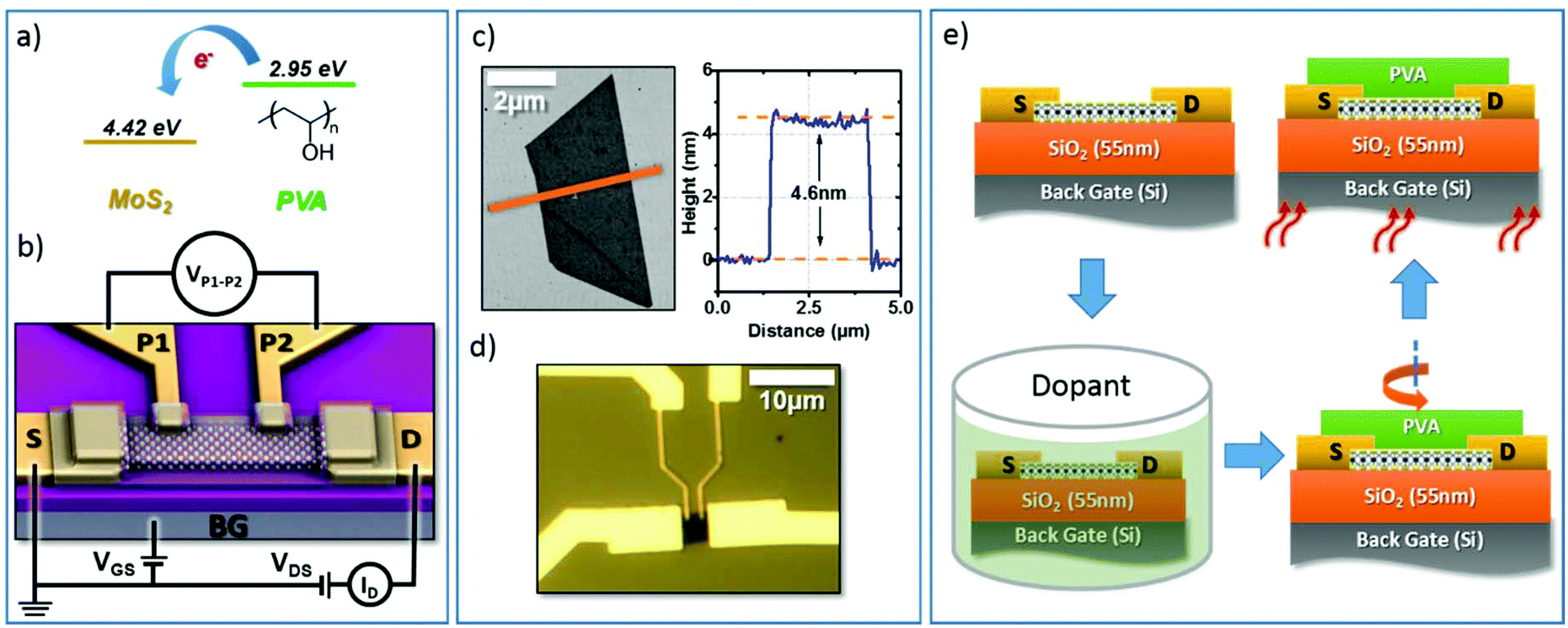 | ||
| Fig. 1 (a) Electron affinity of MoS2 and PVA. (b) Schematic of the device and measurement configuration. (c) AFM of the flake before device fabrication. (d) Optical micrograph of the four terminal back gated device after fabrication. (e) Schematic of the doping process. | ||
After the initial characterization of the as-built device, it was coated with PVA. The device was first submerged in a 0.25% PVA aqueous solution for 1 hour. After that, it was spun at 2000 rpm for 45 s to form a thin film. Next, it was annealed on a hot plate for 5 min at 90 °C to dehydrate the PVA film and then the device was measured immediately. Fig. 1e sketches the procedure for doping the device. The PVA film was then removed by submerging the sample in deionized (DI) water for 1 h at 80 °C and then the doping procedure was repeated with a 1% PVA aqueous solution and characterized. The transfer characteristics of the device before and after PVA doping are shown in Fig. 2a. The ID in the ON state (VGS = 30 V) increased from 19.8 μA μm−1 to 22.1 and 28.3 μA μm−1 and the VTH shifted from −12.1 V in the as-built device to −13.7 V and −14.9 V after doping with PVA concentrations of 0.25% and 1% respectively.
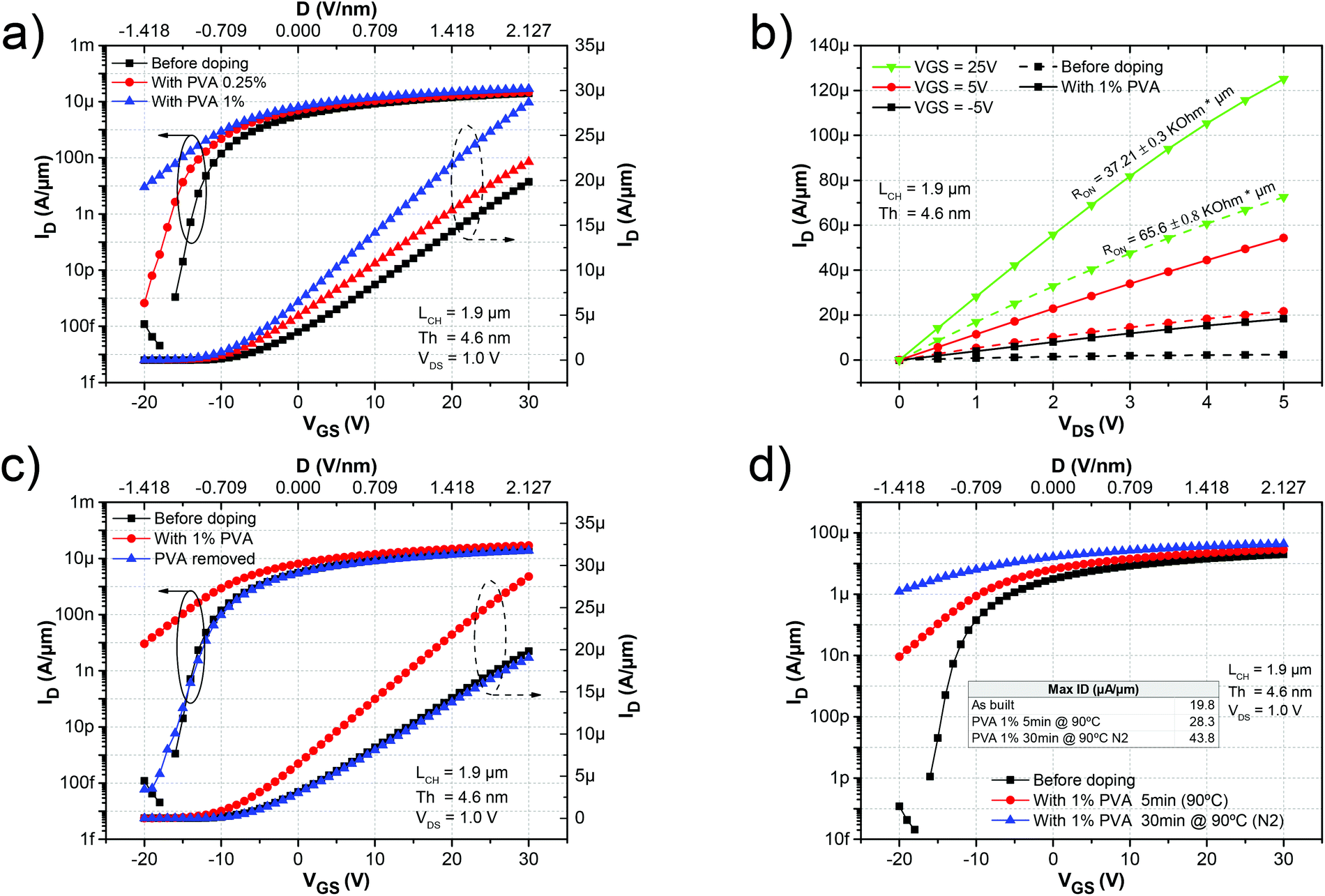 | ||
| Fig. 2 (a) Transfer characteristics of a back-gated MoS2 FET as-built and after doping with 0.25% and 1% PVA and (b) its output characteristics, before (dashed lines) and after (solid lines) doping with PVA 1%. (c) Transfer characteristics before doping, after doping with 1% PVA and after removal of the dopant by immersion in DI water at 80 °C for 1 h. (d) Transfer characteristics of the device before doping, and after doping with PVA 1% under different post-annealing conditions. | ||
As can be seen from the output characteristics of the device (Fig. 2b) the resistance in the ON state (RON) was equally reduced by 43% of its original value from 65.6 kΩ μm to 37.21 kΩ μm due to the increased amount of charge. The monotonic negative shift in VTH and the increase in ID clearly indicated that the MoS2 FET was n-doped.
The extrinsic transconductance of the four probe device was obtained as gm = dID/dVGS without removing the effect of the contact resistance, to serve as a measure of the device performance under normal operational conditions. The peak value of the transconductance (gm,max) for the different stages can be seen in Table 1. Interestingly, upon PVA doping the gm monotonically increases with an approximately 30% increase in the maximum after 1% PVA doping. Compared with the as-built devices this indicates not only an increase in the carrier concentration but also an enhancement of the carrier mobility after functionalization, even under normal operational conditions (extrinsic). For a more precise extraction of the carrier concentration and mobility, the measured channel potential between P1 and P2 (VP1–P2) was used to rule out the effect of the contact resistance. The sheet conductance (GSH) of the device was obtained by GSH = (ID/VP1–P2) × (LP1–P2/WCH). GSH was then used to calculate the intrinsic mobility as μ = 1/COX × dGSH/dVGS where COX (6.28 F cm−2) was obtained considering the dual plate capacitance of 55 nm SiO2 (εr = 3.9). The sheet resistance (RSH) was obtained as 1/GSH. Finally, the two dimensional carrier concentration (n2D) was extracted using n2D = GSH/(qμ), where q is the electron charge. The extracted n2D at VGS = 0 V increased from 2.7 × 1012 cm−2 in the as-built device to 4.0 × 1012 cm−2 after 1% PVA doping which was in agreement with the observed negative shift of VTH. It is also worth noting that the as-built device was already n-doped, which has been reported in previous studies.10,28,29Table 1 compares the extracted device characteristics under the different conditions. It has been demonstrated that passivation can partially alter the doping level of MoS2 by preventing it interacting with the environment.34 However we observed that the strong doping induced in MoS2 after the PVA coating was originated from the interaction between hydroxyl groups of PVA and MoS2 rather than PVA passivation characteristics (see the ESI† for further details).
| n 2D (VGS = 0 V) (×1012 cm−2) | g m (extrinsic) (μS μm−1) | Mobility (intrinsic) (cm2 V−1 s−1) | R SH (VGS = 0 V) (kΩ □−1) | Max ID (VDS = 1 V) (μA μm−1) | |
|---|---|---|---|---|---|
| a After annealing for 30 min at 90 °C. | |||||
| As built | 2.65 | 0.6 | 20.1 | 161.0 | 19.8 |
| 0.25% PVA | 3.84 | 0.59 | 20 | 66.5 | 22.1 |
| 1% PVA | 4.04 | 0.77 | 27.9 | 57.6 | 28.3 |
| 1% PVAa | 7.98 | 1.04 | 36.6 | 20.3 | 43.8 |
Fig. 2c plots the transfer characteristics of the devices before doping, after doping with 1% PVA, and then after removing the water soluble PVA film by submerging it in 80 °C DI water. Interestingly, the device completely recovers to its original state after removal of the PVA film by the DI water, demonstrating the non-destructive nature of the doping process. Additionally, this can also allow for selective area doping of the device.
Next, we analysed the effect of dehydration of the PVA on the device performance. The MoS2 device doped with 1% PVA was annealed for 30 min at 90 °C under an N2 atmosphere. As shown in Fig. 2d, ID increased considerably from 28.3 μA μm−1 when annealed for 5 min (red circles) to 43.8 μA μm−1 when annealed for 30 min (blue triangles). The n2D also increased from 4.04 × 1012 cm−2 to 7.98 × 1012 cm−2 at VGS = 0 V by increasing the annealing time from 5 to 30 min. No further increase was observed above 30 min. The increase in current after doping and annealing is also followed by a reduction in the ION/OFF ratio of the device, as can be seen from Fig. 2a and d. One way to increase the ION/OFF ratio is by selectively doping only the access region close to the contact instead of the entire channel. This is demonstrated later in this manuscript. Additionally, a monotonic increase of the intrinsic mobility can be observed in Table 1 for the different concentrations of PVA.
The electrons in the PVA that contribute to charge transfer originate from the hydroxyl groups of the polymer. However, any absorbed water in the PVA film will be tightly immobilized around the available hydroxyl groups through hydrogen bonding.35 This immobilized water effectively screens the electron charge transfer from the PVA to the MoS2 film. Therefore, when less water is present in the film (corresponding to a longer annealing time), more charge transfer can take place, which consequently results in an enhanced ON state ID (Fig. 2d). Furthermore, the additional increase in mobility after dehydrating the film can be explained by both the screening of charge impurities by the PVA film and the additional injected charges. Additionally, PVA tends to form a semi-crystalline structure by creating a double layer of molecules held together by hydrogen bonds while weak van der Waals forces operate between the double layers36,37 (see the ESI† for X-ray diffraction (XRD) spectra). This semi-crystalline structure is altered by the presence of water molecules that disrupt the inter-PVA hydrogen bonds, creating a more amorphous structure.37 The ordering of the PVA molecules allows for more effective screening of both the charged impurities and surface optical phonon scattering. Similar increases in the mobility by the screening of charged impurities were previously demonstrated for the case of high k dielectric encapsulation,9 PMMA38 and for ionic liquids.39 This increase in the mobility together with the increase in the carrier concentration also contributes to reducing the value of the sheet resistance from 161.0 kΩ sq−1 to 20.3 kΩ sq−1 as can be seen in Table 1 at VGS = 0 V (as will be in the case for non-gated access regions).
The impact of the PVA doping on the contact resistance was then assessed using the transmission line measurement (TLM) technique with channel lengths of 100, 800 and 1900 nm. The devices were characterized before doping and were then doped with 1% PVA. The devices were annealed for 30 min at 90 °C under N2 and were characterized again. The transfer characteristics of the device with the smallest channel (LCH = 100 nm) before and after doping can be seen in Fig. 3a. The increase of the ION and gm (shown in the inset of Fig. 3a) after PVA coating demonstrates that the device has been doped and the mobility has increased. To extract the RC, the total resistance (RTOTAL), normalized with respect to WCH, for each device was modelled to be RTOTAL = 2RC + RSH × LCH, where the last term gives the resistance of the channel. The RTOTALvs. the LCH plot was linearly fitted with the extrapolated value at LCH = 0 equal to 2RC and the slope of the line equal to RSH. This process is repeated for each VGS value. Fig. 3b compares RCvs. VGS of the device before and after 1% PVA coating. The RC before doping at VGS = 24 V was 3.1 ± 0.18 kΩ μm which decreased by approximately 30% to 2.1 ± 0.14 kΩ μm after PVA doping. This reduction can be explained by the decrease in the sheet resistance of the MoS2 film close to the contact area and the further thinning of the SB barrier by the degenerate doping induced by the PVA coating. Similar observations with different doping concepts have been observed in the literature.31 It is also important to note that RC is reduced by a factor of approximately 5 at VGS = 0 V, thus even without any gate potential applied (as is the case of non-overlapping gate devices) the contact resistance is greatly reduced.
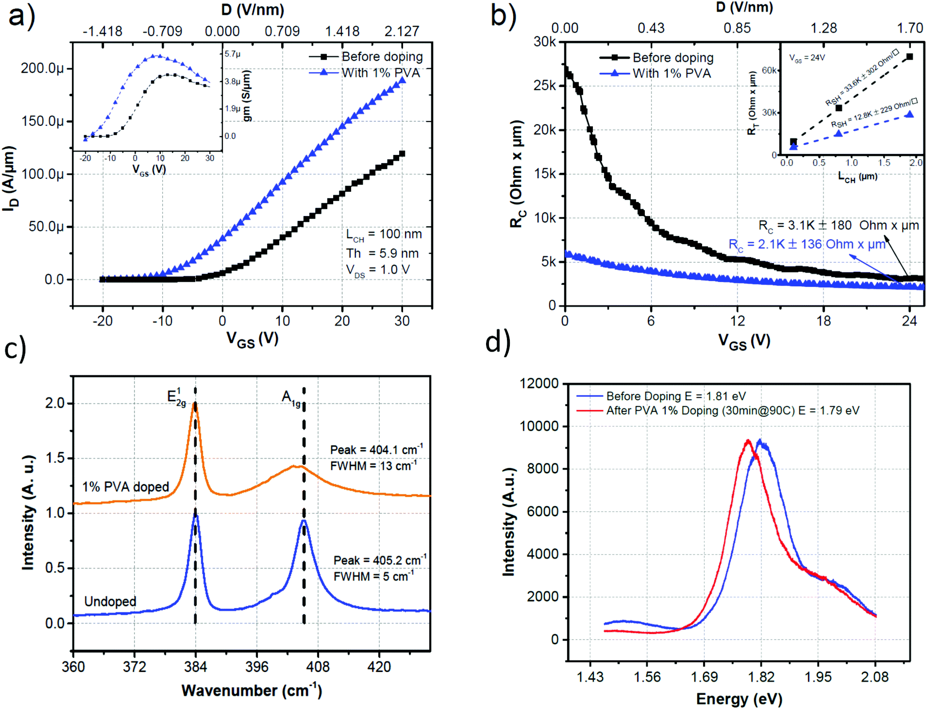 | ||
| Fig. 3 (a) Transfer characteristics of a MoS2 FET with a channel length LCH = 100 nm before (black) and after doping with 1% PVA and annealing for 30 min under an N2 atmosphere (blue). (b) Contact resistance as a function of the gate voltage before (black) and after doping with 1% PVA and annealing for 30 min at 90 °C under N2 (blue). The values were extracted from the total resistance of three devices with different channel lengths (100 nm, 800 nm and 1.9 μm) using the TLM technique. The inset shows the TLM results at VGS = 24 V. (c) Raman spectra before and after doping showing quenching and a small redshift of the A1g peak as expected from the increase of electrons. (d) Photoluminescence spectra before and after doping. A red shift after doping is also indicative of the increase of the electron concentration. | ||
The doping of the MoS2 film was further confirmed by Raman spectroscopy. The Raman spectra of a MoS2 film before and after doping with 1% PVA followed by annealing for 30 min under an N2 atmosphere are shown in Fig. 3c. The MoS2 flake before doping had signature peaks for the basal-plane vibrations of the molybdenum atoms (E2g1) at around 384.1 cm−1 and the vertical vibrations of the sulphur atoms (A1g) at around 405.2 cm−1. After doping a shift toward a lower wavenumber (404.1 cm−1) can be seen for the A1g peak. There was also broadening of the full width at half maximum (FWHM) from 5 to 13 cm−1. These observations can be attributed to the high electron–phonon coupling of the A1g mode.40 The shift in the frequency is linked to the occupation of antibonding states in the conduction bands that weakens the S–Mo bonds. The FWHM broadening, on the other hand, can be linked to the increase in the electron–phonon coupling. The E2g1 remained almost unchanged, which was expected given its weak electron–phonon coupling compared to the A1g mode. Photoluminescence was also used to corroborate the doping (Fig. 3d). The red shift of the photoluminescence peak indicates an increase in the electron concentration. This increase in electrons enhances the contribution of trions (electron–electron–hole excitations) to the photoluminescence of the device. These results are comparable to the reported values using different electron dopant molecules.29
But, as mentioned earlier, after doping it is more difficult to turn the device off owing to the high fields required to deplete the charge injected by the PVA film. This can be avoided by doping only the access regions of the device and the areas near the contact while avoiding injection of the same number of carriers to the channel. In Fig. 4a, a scheme of such a device concept is presented where one device is covered with a 1 μm-thick photoresist and then patterned with photolithography to cover only a portion of the channel. The transfer characteristics of the device without and with the insulation layer (Fig. 4b) suggest that little change is induced in the device by the insulation layer. After the insulation layer is properly patterned, the device is functionalized with PVA following the previously described procedure and annealed for 30 min at 90 °C under an N2 atmosphere. As can be seen in Fig. 4b, after doping, the ON current increases from 4.1 μA μm−1 to 8.6 μA μm−1. Thus the improvement is comparable to previous cases, as shown in Table 1, where the current increases from 19.8 μA μm−1 to 43.8 μA μm−1, with the difference that now we are able to turn off the device and the ION/OFF remains about the same as that observed before doping.
 | ||
| Fig. 4 (a) Schematic of the process for channel isolation to avoid full doping of the channel and the optical micrograph of the final device. (b) Transfer characteristics of the as-built device after patterning the 1 μm insulation layer and after functionalization with PVA. When the insulation layer is present, the channel is less doped and it is possible to turn off the device, thus the ION/OFF ratio remains ∼7 orders of magnitude even after doping. | ||
Additionally, the stability of the PVA functionalization was studied. The degradation of the performance as a function of time in an ambient environment is shown in Fig. 5a. As expected from a water soluble polymer, PVA tends to trap water and, as explained previously, this trapped water degrades the effectiveness and stability of the doping mechanism. It can be seen that the degradation is improved after annealing for 30 min at 90 °C; nevertheless, the definitive robustness of the PVA functionalization is only achieved after encapsulation by Al2O3 ALD, as demonstrated in Fig. 5b. Encapsulation is a normal process performed in the semiconductor industry to protect electronic devices from humidity and other contaminants. Interestingly, this also demonstrates that the PVA film resists the deposition of the Al2O3 20 nm film by atomic layer deposition (ALD) without degradation at 150 °C.
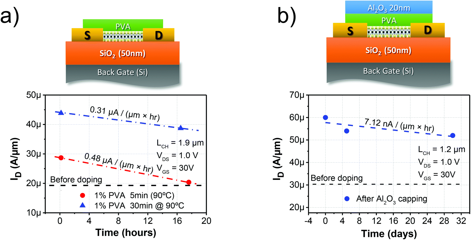 | ||
| Fig. 5 Schematic and performance degradation of the uncapped device before and after annealing (a) and after encapsulation with 20 nm Al2O3 (b). The robustness of the device toward the environment was increased after annealing, and greatly improved after encapsulation achieving high stability. | ||
Conclusions
We have demonstrated strong n-type doping of MoS2 FETs using a PVA coating. The n2D at VGS = 0 V was modulated in the range of 2.6 × 1012 cm−2 to 4.0 × 1012 cm−2 by applying a PVA coating with a concentration increasing up to 1%. n2D was further increased to 8.65 × 1012 cm−2 by dehydrating the PVA film under an N2 flow. The increase in the doping of the MoS2 film reduced the contact resistance by 30% from its original value. The RSH was reduced upon doping from 161 kΩ sq−1 to 20 kΩ sq−1. The doping approach enables a threshold modulation in the range of −12.1 V to −24.9 V and because of the non-covalent nature of the PVA–MoS2 interaction, the doping is completely reversible. Also, the transconductance was enhanced by a factor of approximately 2 and the intrinsic mobility increased from 19.7 cm2 V−1 s−1 up to a value of 36.6 cm2 V−1 s−1 when the PVA-doped device was allowed to rest under N2. The mobility increase, together with the increase in the carrier concentration, gives an ION up to approximately 43 μA μm−1, showing approximately a 200% increase compared to the value obtained from the undoped sample. The enhanced field-effect transconductance and mobility can potentially lead to the application of MoS2-based devices in high performance electronics. Additionally, the PVA functionalization was used to selectively dope the access regions of the MoS2 channel allowing improvement in the performance of the device while still having an ION/OFF of more than 7 orders of magnitude. Furthermore, it was demonstrated that the PVA functionalization resists the ALD deposition of a 20 nm Al2O3 film and that after encapsulation it is very robust towards the environment.Methods
The MoS2 films were mechanically exfoliated from bulk crystals supplied by Nano Instruments Inc. onto a substrate with 55 nm of SiO2 that was thermally grown on highly n-doped Si. The electrodes were patterned using electron beam lithography with a PMMA/LOR-1A resist. 70 nm of Au was then deposited and lifted off to pattern the electrodes. The PVA solutions were prepared by diluting 98% hydrolysed PVA from Sigma-Aldrich in water at 80 °C with stirring until it was dissolved. The electrical measurements were carried out with a Keithley 4200-SCS parameter analyser in a chamber with an adjustable N2 flow.Acknowledgements
The authors wish to thank R. Murray for his valuable help in reviewing the manuscript and the laboratory personnel, J. Loo, K. Baumans, and J. De Cooman for their excellent technical work. A. Nourbakhsh acknowledges a research fellowship from the Research Foundation-Flanders, Belgium (FWO). The authors would also like to thank imec beyond the CMOS program for financial support.References
- B. Radisavljevic, A. Radenovic, J. Brivio, V. Giacometti and A. Kis, Nat. Nanotechnol., 2011, 6, 147–150 CrossRef CAS PubMed.
- H. Fang, S. Chuang, T. C. Chang, K. Takei, T. Takahashi and A. Javey, Nano Lett., 2012, 12, 3788–3792 CrossRef CAS PubMed.
- D. De, J. Manongdo, S. See, V. Zhang, A. Guloy and P. Haibing, Nanotechnology, 2013, 24, 025202 CrossRef PubMed.
- A. Splendiani, L. Sun, Y. Zhang, T. Li, J. Kim, C.-Y. Chim, G. Galli and F. Wang, Nano Lett., 2010, 10, 1271–1275 CrossRef CAS PubMed.
- S. Kim, A. Konar, W.-S. Hwang, J. H. Lee, J. Lee, J. Yang, C. Jung, H. Kim, J.-B. Yoo and J.-Y. Choi, et al. , Nat. Commun., 2012, 3, 1011 CrossRef PubMed.
- Y. Yoon, K. Ganapathi and S. Salahuddin, Nano Lett., 2011, 11, 3768–3773 CrossRef CAS PubMed.
- H. Liu, A. T. Neal and P. D. Ye, ACS Nano, 2012, 6, 8563–8569 CrossRef CAS PubMed.
- W. Zhu, T. Low, Y.-H. Lee, H. Wang, D. B. Farmer, J. Kong, F. Xia and P. Avouris, Nat. Commun., 2013, 5, 3087 Search PubMed.
- H. Wang, L. Yu, Y.-H. Lee, Y. Shi, A. Hsu, M. L. Chin, L.-J. Li, M. Dubey, J. Kong and T. Palacios, Nano Lett., 2012, 12, 4674–4680 CrossRef CAS PubMed.
- B. Radisavljevic and A. Kis, Nat. Mater., 2013, 12, 815–820 CrossRef CAS PubMed.
- S. Bertolazzi, D. Krasnozhon and A. Kis, ACS Nano, 2013, 7, 3246–3252 CrossRef CAS PubMed.
- D. Xiao, G.-B. Liu, W. Feng, X. Xu and W. Yao, Phys. Rev. Lett., 2012, 108, 196802 CrossRef PubMed.
- H. Zeng, J. Dai, W. Yao, D. Xiao and X. Cui, Nat. Nanotechnol., 2012, 7, 490–493 CrossRef CAS PubMed.
- S. Wi, H. Kim, M. Chen, H. Nam, L. J. Guo, E. Meyhofer and X. Liang, ACS Nano, 2014, 8, 5270–5281 CrossRef CAS PubMed.
- S. Das, H.-Y. Chen, A. V. Penumatcha and J. Appenzeller, Nano Lett., 2013, 13, 100–105 CrossRef CAS PubMed.
- I. Popov, G. Seifert and D. Tománek, Phys. Rev. Lett., 2012, 108, 156802 CrossRef PubMed.
- A. Dankert, L. Langouche, M. V. Kamalakar and S. P. Dash, ACS Nano, 2014, 8, 476–482 CrossRef CAS PubMed.
- W. Park, Y. Kim, S. K. Lee, U. Jung, J. H. Yang, C. Cho, Y. Kim, S. K. Lim, I. S. Hwang and H.-B.-R. Lee, et al. , Int. Electron Devices Meet., 2014, 5.1, 108–111 Search PubMed.
- C. Gong, C. Huang, J. Miller, L. Cheng, Y. Hao, D. Cobden, J. Kim, R. S. Ruoff, R. M. Wallance and K. Cho, et al. , ACS Nano, 2013, 7, 11350–11357 CrossRef CAS PubMed.
- L. Wang, I. Meric, P. Y. Huang, Q. Gao, H. Tran, T. Taniguchi, K. Watanabe, L. M. Campos, D. A. Muller, J. Guo, P. Kim, J. Hone, K. L. Shepard and C. R. Dean, Science, 2013, 343, 614–617 CrossRef PubMed.
- C. Lockhart, G. Arutchelvan, I. Radu, D. Lin, C. Huyghebaert, M. Heyns and S. De Gendt, ECS J. Solid State Sci. Technol., 2016, 5, 3072–3081 CrossRef.
- K. Dolui, I. Rungger, C. D. Pemmaraju and S. Sanvito, Phys. Rev. B: Condens. Matter, 2013, 88, 075420 CrossRef.
- H.-P. Komsa, J. Kotakoski, S. Kurasch, O. Lehtinen, U. Kaiser and A. V. Krasheninnikov, Phys. Rev. Lett., 2012, 109, 035503 CrossRef PubMed.
- M. Chen, H. Nam, S. Wi, L. Ji, X. Ren, L. Bian, S. Lu and X. Liang, Appl. Phys. Lett., 2013, 103, 142110 CrossRef.
- L. Yang, K. Majumdar, H. Liu, Y. Du, H. Wu, M. Hatzistergos, P. Y. Hung, R. Tieckelmann, W. Tsai, C. Hobbs and P. D. Ye, Nano Lett., 2014, 14, 6275–6280 CrossRef CAS PubMed.
- P. Blake, P. D. Brimicombe, R. R. Nair, T. J. Booth, D. Jiang, F. Schedin, L. A. Ponomarenko, S. V. Morozov, H. F. Gleeson and E. W. Hill, et al. , Nano Lett., 2008, 8, 1704–1708 CrossRef PubMed.
- S. Bae, H. Kim, Y. Lee, X. Xu, J.-S. Park, Y. Zheng, J. Balakrishnan, T. Lei, H. T. Kim, Y. I. Song, T.-J. Kim, K. S. Kim, B. Özyilmaz, J.-H. Ahn, B. H. Hong and S. Iijima, Nat. Nanotechnol., 2010, 132, 574–578 CrossRef PubMed.
- H. Fang, M. Tosun, G. Seol, T. C. Chang, K. Takei, J. Guo and A. Javey, Nano Lett., 2013, 13, 1991–1995 CrossRef CAS PubMed.
- Y. Li, C.-Y. Xu, H. Ping An and L. Zhen, ACS Nano, 2013, 7, 7795–7804 CrossRef CAS PubMed.
- Y. Du, H. Liu, A. T. Neal, M. Si and P. D. Ye, IEEE Electron Device Lett., 2013, 34, 1328–1330 CrossRef CAS.
- D. Kiriya, M. Tosun, P. Zhao, J. S. Kang and A. Javey, J. Am. Chem. Soc., 2014, 136, 7853–7856 CrossRef CAS PubMed.
- M. El-Masy, E. Sheha, K. Patel and G. Sharma, Optik, 2013, 124, 1624–1631 CrossRef.
- L. A. King, W. Zhao, M. Chhowalla, D. J. Riley and E. Goky, J. Mater. Chem. A, 2013, 1, 8935 RSC.
- D. Yue, D. Lee, Y. D. Jang, M. S. Choi, H. J. Nam, D. Y. Jung and W. J. Yoo, Nanoscale, 2016, 8, 12773–12779 RSC.
- R. M. Hodge, G. H. Edward and G. P. Simon, Polymer, 1996, 37, 1371–1376 CrossRef CAS.
- H. E. Assender and A. H. Windle, Polymer, 1997, 39, 4295–4302 CrossRef.
- N. A. Peppas, Eur. Polym. J., 1975, 12, 495–498 CrossRef.
- W. Bao, X. Cai, D. Kim, K. Sridhara and M. S. Fuhrer, Appl. Phys. Lett., 2013, 102, 042104 CrossRef.
- M. M. Perera, M.-W. Lin, H.-J. Chuang, B. P. Chamlagain, C. Wang, X. Tan, M. M.-C. Cheng, D. Tománek and Z. Zhou, ACS Nano, 2013, 7, 449–4458 CrossRef PubMed.
- B. Chakraborty, A. Bera, D. V. S. Muth, S. Bhowmick, U. V. Waghmare and A. K. Sood, Phys. Rev. B: Condens. Matter, 2012, 85, 161403 CrossRef.
Footnotes |
| † Electronic supplementary information (ESI) available: Electrical characterization of a PVA film, current behaviour of PVA-doped MoS2 FETs under humid conditions, photoluminescence of MoS2 before and after doping, spectroscopy characterization of PVA films and analysis of the MoS2 film thickness, environment and passivation effects on the device. See DOI: 10.1039/c6nr06980k |
| ‡ With imec at the time of this work; currently with Massachusetts Institute of Technology, Cambridge, Massachusetts 02139, USA. |
| This journal is © The Royal Society of Chemistry 2017 |