
Carbon-doped freestanding TiO2 nanotube arrays in dye-sensitized solar cells†
Won-Yeop
Rho‡
ab,
Ho-Sub
Kim‡
b,
Hyung-Mo
Kim
a,
Jung Sang
Suh
b and
Bong-Hyun
Jun
*a
aDepartment of Bioscience and Biotechnology, Konkuk University, Seoul 143-701, Republic of Korea. E-mail: bjun@konkuk.ac.kr
bDepartment of Chemistry, Seoul National University, Seoul 151-747, Republic of Korea
First published on 21st November 2016
Abstract
Dye-sensitized solar cells (DSSCs) were fabricated with both closed- and open-ended freestanding TiO2 nanotube arrays that were doped with carbon via chemical vapor deposition to improve their electron transport properties. The energy conversion efficiencies of DSSCs increased from 5.07% to 6.21% after doping with a small amount of carbon, i.e., an enhancement of 22.4%. This suggests that the π–π conjugation introduced by carbon doping improved the efficiency of electron transport. However, energy conversion efficiencies of DSSCs with a large amount of carbon doping on the TiO2 nanotube arrays decreased from 5.07% to 2.87%, with a lower short-circuit current, open circuit voltage, and fill factor because of the reduced level of dye adsorption on the TiO2 nanotube arrays.
Introduction
Dye-sensitized solar cells (DSSCs) have been extensively researched because of their high energy conversion efficiencies and low cost.1–3 Recently, mesoporous TiO2 nanoparticle (NP) films have been widely used for DSSCs. However, their efficiencies have been limited because of grain boundaries, defects, and innumerous trapping sites that can cause charge recombination and low electron mobility.TiO2 nanotubes have great potential to overcome the problems of TiO2 NP films because their unique structure enhances electron transport and charge separation by forging direct pathways and accelerating charge transfer between interfaces.4–15 TiO2 nanotube arrays obtained from electrochemical anodization are good candidates for rapid electron-transport of materials with reduced charge recombination because of their highly ordered vertically oriented tubular structures, which gives them a number of advantages over TiO2 NP films.16–19 Although DSSCs based on TiO2 nanotube arrays have high potential for improved energy conversion efficiencies, to date DSSCs based on closed-ended TiO2 nanotube arrays have shown lower energy conversion efficiencies than DSSCs based on TiO2 NP films. Recently, we demonstrated that open-ended TiO2 nanotube arrays where the barrier layers have been removed provide higher energy conversion efficiencies for DSSCs.11
Carbon doping has been considered to be a promising means of improving charge separation and electron transport in solar cells owing to the good electrical properties imparted by π–π conjugation. The Han and Li groups have both reported that carbon nanotube composite films with TiO2 NPs showed enhanced electron transport,20,21 and the Gao and Lee groups reported that graphene composite films on photoelectrodes showed improved energy conversion efficiency.22,23 However, it is not easy to incorporate carbon materials into well-ordered vertically aligned TiO2 nanotube arrays except via the direct growth of carbon materials.
Here, we report that carbon-doped TiO2 nanotube arrays were used as photoanodes for DSSCs to increase energy conversion efficiency by improving charge separation and electron transport. The carbon was doped on either closed- or open-ended TiO2 nanotube arrays by chemical vapor deposition (CVD). The performances of the DSSCs fabricated with the closed- and open-ended TiO2 nanotube arrays with and without carbon doping were compared to study the influence of carbon doping on the energy conversion efficiency of DSSCs.
Experimental
Preparation of closed- or open-ended TiO2 nanotube arrays
TiO2 nanotube arrays were fabricated by anodizing titanium foils (Alfa Aesar, 99.7% purity, 2.5 cm × 4.0 cm × 320 μm). Carbon rods were used as the cathode. The electrolyte was composed of 0.8 wt% NH4F and 2 vol% H2O in ethylene glycol at 25 °C. A 60 V DC potential was applied to the anodization system for 2 h. The TiO2 nanotube arrays formed on the Ti foil were annealed at 450 °C for 1 h. After the sample was cooled to room temperature, a second anodization was performed on the annealed samples at 30 V for 10 min. The sample was then placed in 10% H2O2 for 24 h to detach the nanotubes from the Ti foil. The process of opening the bottom layer (the closed-ended tip) of the TiO2 nanotube arrays was performed by ion milling with Ar+ bombardment.Synthesis of carbon-doped closed- or open-ended TiO2 nanotube arrays on FTO glass
Fluorine doped tin oxide (FTO) glass was used as the electrode and the supporting substrate for TiO2 nanotube arrays. Titanium diisopropoxide bis(acetylacetonate) (5 wt% in n-butanol) was injected and spin-coated onto the washed FTO glass. The samples were annealed at 450 °C for 1 h to form a compact TiO2 blocking layer. To attach TiO2 nanotube arrays, TiO2 paste (Solaronix, T/SP) was applied to the FTO glass using the doctor-blade method. The closed- or open-ended TiO2 nanotube arrays were then introduced into the TiO2 paste. The samples were annealed at 450 °C for 30 min, then placed in a quartz furnace tube that was filled with nitrogen (200 sccm). At the required times, hydrogen and ethylene were injected into the tube at 450 °C and flow rates of 30 and 40 sccm, respectively.Fabrication of dye-sensitized solar cells
Dye molecules were adsorbed onto photoanodes consisting of carbon-doped or non-doped TiO2 nanotube arrays (open-ended or closed-ended) using 0.5 mM solutions of N719 ((Bu4N)2Ru(dobpyH)2(NCS)2, Solaronix) in absolute ethanol at 50 °C for 8 h. The samples were washed several times with absolute ethanol by immersing for 10 min to remove extra physisorbed dye molecules from the TiO2 nanotube arrays. Counter electrodes were fabricated by drop-casting chloroplatinic acid (H2PtCl6) in ethanol onto the FTO glass. A 60 μm-thick hot-melt Surlyn spacer (Solaronix) was placed between the photoanode and the counter electrode, and the electrolyte was composed of 0.7 M 1-butyl-3-methyl-imidazolium iodide (BMII), 0.03 M I2, 0.1 M guanidium thiocyanate (GSCN), and 0.5 M 4-tert-butyl pyridine (TBP) in a mixture of acetonitrile and valeronitrile (85![[thin space (1/6-em)]](https://www.rsc.org/images/entities/char_2009.gif) :15 v/v). The electrolyte was injected into the gap between the electrodes, and the cells were sealed to prevent the electrolyte from leaking.
:15 v/v). The electrolyte was injected into the gap between the electrodes, and the cells were sealed to prevent the electrolyte from leaking.
Characterization of dye-sensitized solar cells
The structures of the closed- and open-ended TiO2 nanotube arrays with and without carbon doping were analyzed using a field emission scanning electron microscope (FE-SEM, JSM-6700F, JEOL Ltd). Current density–voltage measurements were performed using an electrometer (Keithley 2400) under AM 1.5 illumination (100 mW cm−2) provided by a solar simulator (1 kW xenon with AM 1.5 filter, PEC-L01, Peccel Technologies). Electrochemical impedance spectroscopy (EIS) was performed using a potentiostat (Solartron 1287) equipped with a frequency response analyzer (Solartron 1260) between 10−2 and 106 Hz, and were analyzed using Z-View software (Solartron Analytical) with the aid of an appropriate equivalent circuit. The applied bias voltage and the AC amplitude were set at the open circuit voltage (Voc) of the DSSCs and 10 mV, respectively. The impedance measurements were carried out at open-circuit potential under one sun of AM 1.5 light illumination.Results and discussion
Fig. 1 shows the fabrication of DSSCs containing carbon-doped TiO2 nanotube arrays. First, TiO2 nanotube arrays were prepared by anodization, as shown in Fig. 1A(a). To yield crystalline TiO2 nanotube arrays, the substrate was annealed and then a second anodization step was performed to prepare freestanding TiO2 nanotube arrays, as shown in Fig. 1A(b). The resulting freestanding TiO2 nanotube arrays were transferred onto FTO glass with TiO2 paste that was coated onto the FTO glass using a doctor blade and then sintered under ambient conditions, as shown in Fig. 1A(c). Carbon was then synthesized by CVD using ethylene gas, with the coating time being used to control the level of doping. The dye (N719) was then adsorbed onto the TiO2 nanotube arrays. DSSCs were fabricated by assembly of the working electrode (TiO2 nanotube arrays) and the counter electrode (Pt), as shown in Fig. 1B.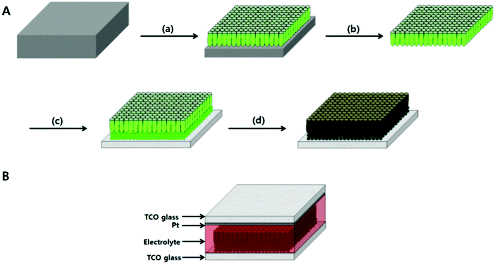 | ||
| Fig. 1 Overall scheme showing fabrication of DSSCs based on TiO2 nanotube arrays. (A) (a) First anodization and annealing step, (b) second anodization and detachment from Ti foil to yield freestanding TiO2 nanotube arrays, (c) transfer of freestanding TiO2 nanotube arrays to FTO glass, and (d) carbon doping on TiO2 nanotube arrays by CVD. (B) Structure of a DSSC. | ||
Fig. 2 shows FE-SEM images of the top, side, and bottom views of freestanding TiO2 nanotube arrays. The upper pore size was approximately 100 nm, as can be seen in Fig. 2a, and the length of the freestanding TiO2 nanotube arrays was around 20 μm, as shown in Fig. 2b. Fig. 2c shows the bottom layer of the TiO2 nanotube arrays which was detached from the Ti foil after anodization, which resulted in closed-ended TiO2 nanotube arrays. The bottom layer of the TiO2 nanotube arrays could be removed by using a physical etching method such as ion milling,11 with the bottom pore size of the resulting open-ended TiO2 nanotube arrays being approximately 50 nm, as shown in Fig. 2d. The DSSCs were prepared with closed- or open-ended TiO2 nanotube arrays that had been doped with carbon materials to improve electron transport.
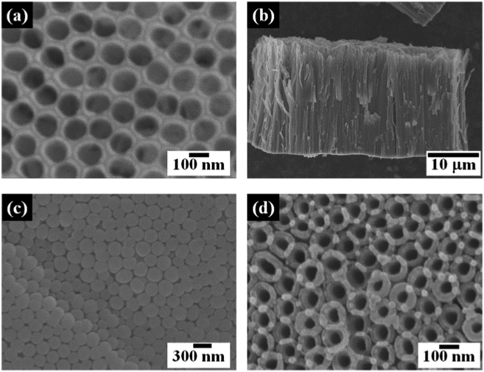 | ||
| Fig. 2 FE-SEM images of TiO2 nanotube arrays from (a) top, (b) side, and (c) bottom views. The bottoms of the tubes after ion milling are shown in (d). | ||
Raman spectra of TiO2 nanotube arrays and carbon-doped TiO2 nanotube arrays between 380 and 1800 cm−1, which can be used to characterize the carbon and TiO2 structures present, are shown in Fig. 3. The B1g (395 cm−1), A1g (515 cm−1) and Eg (635 cm−1) peaks in the Raman spectrum shown in Fig. 3a indicate that the TiO2 was in the form of an anatase structure.24 After carbon materials were synthesized by CVD, the anatase TiO2 peaks were maintained and some narrow bands were formed. The G band at 1586 cm−1 represents graphite, while the D band at 1370 cm−1 was caused by the disorderly network of sp2 and sp3 carbon clusters. The intensity ratio of D and G bands was about 0.75, suggesting the presence of π–π conjugation from the sp2 sites on the carbon materials. This would lead to more efficient electron transport in DSSCs.
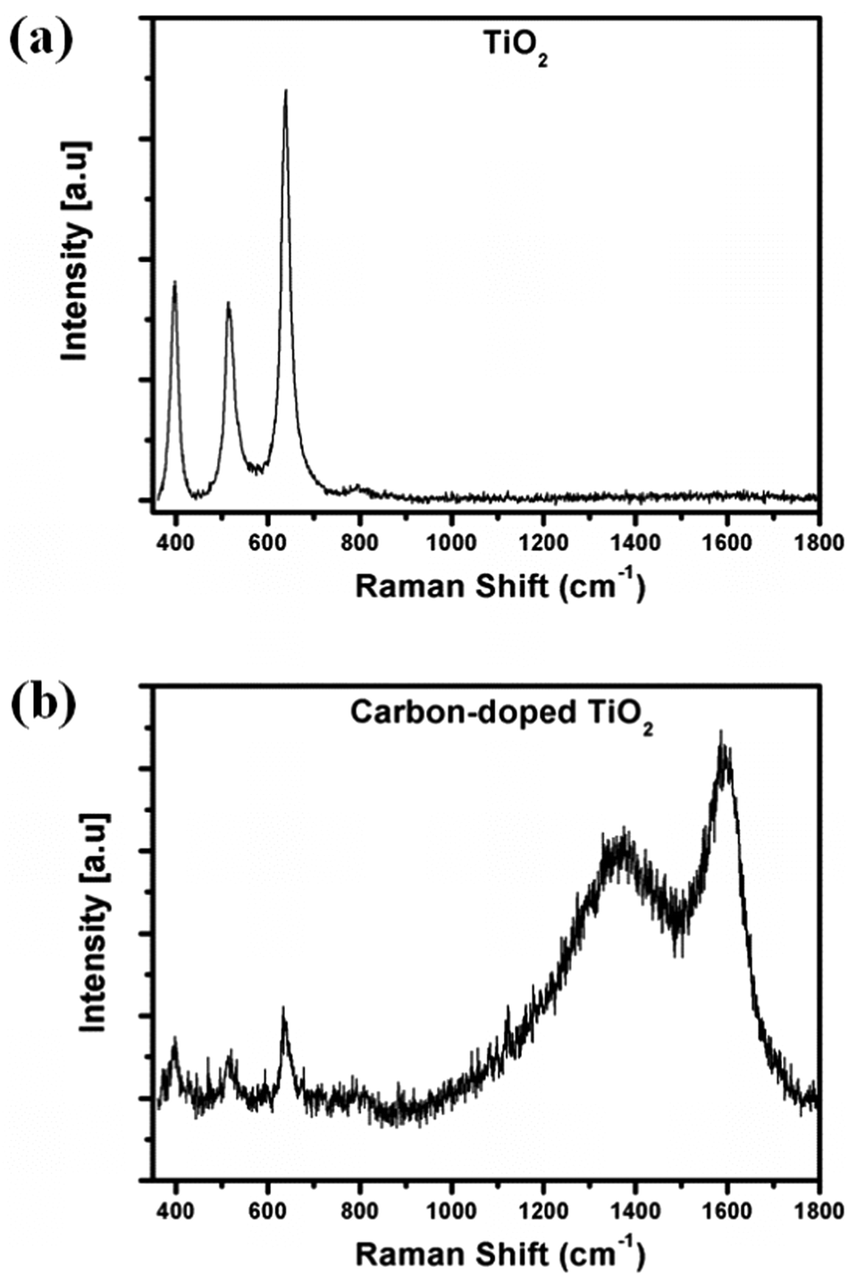 | ||
| Fig. 3 Raman spectra of (a) TiO2 nanotube arrays and (b) carbon-doped TiO2 nanotube arrays. | ||
Fig. 4 presents the current density–voltage curves of three different DSSCs based on closed-ended TiO2 nanotube arrays that were attached to FTO glass using TiO2 paste, as measured under AM 1.5 sunlight. The open circuit voltages (Voc), short-circuit currents (Jsc), fill factors (ff), and energy conversion efficiencies (η) of the DSSCs based on closed-ended TiO2 nanotube arrays are summarized in Table 1. For the DSSC using undoped TiO2, the energy conversion efficiency was 4.19%, while when carbon doping was performed on the TiO2via CVD for 30 s, the energy conversion efficiency improved significantly from 4.19% to 5.16%, corresponding to a 23.15% enhancement. However, when carbon doping was performed for 60 s, the energy conversion efficiency decreased from 4.19% to 2.27%, corresponding to 45.82% suppression in the energy conversion efficiency. The dye loading of the closed-ended TiO2 nanotube array was 145 nmol cm−2, which was higher than that of the cells with TiO2 that had been carbon doped for 30 s and 60 s. Compared with the DSSC using undoped TiO2 nanotube arrays, the Jsc of the cell using TiO2 that had been carbon doped for 30 s increased from 7.46 mA cm−2 to 9.69 mA cm−2, corresponding to a 28.89% enhancement in spite of the slightly reduced dye loading of 140 nmol cm−2, indicating that electron transport was improved by carbon doping. However, the ff decreased slightly due to the increase in recombination caused by π–π conjugation in the carbon materials. When TiO2 was doped with a large amount of carbon, the Jsc decreased remarkably from 7.46 mA cm−2 to 5.08 mA cm−2 due to the reduced dye absorption. When larger amounts of carbon materials are doped on closed-ended TiO2 nanotube arrays, the dye loading decreased to 89 nmol cm−2, indicating that the binding between the dye and the surface of the TiO2 nanotube arrays was disturbed. Moreover, the ff also decreased, indicating that there was a large degree of π–π conjugation in the carbon materials.
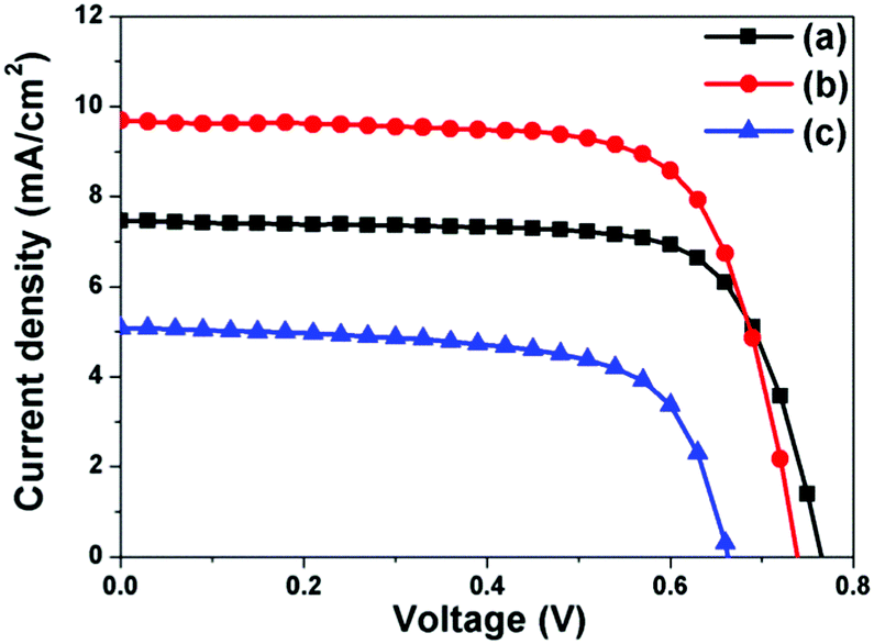 | ||
| Fig. 4 Current density–voltage curves of DSSCs with closed-ended TiO2 nanotube arrays (a) without carbon doping, and with carbon doping via CVD for (b) 30 s and (c) 60 s. | ||
| DSSCs based on closed-ended TiO2 nanotube arrays | J sc (mA cm−2) | V oc (V) | ff | η (%) | Dye loading (nmol cm−2) |
|---|---|---|---|---|---|
| No carbon doping | 7.46 | 0.77 | 0.73 | 4.19 | 145 |
| Carbon doping for 30 s | 9.69 | 0.74 | 0.72 | 5.16 | 140 |
| Carbon doping for 60 s | 5.08 | 0.66 | 0.67 | 2.27 | 89 |
Fig. 5 presents the current density–voltage curves of three different DSSCs based on open-ended TiO2 nanotube arrays measured under AM 1.5 sunlight. The open circuit voltages (Voc), short-circuit currents (Jsc), fill factors (ff), and energy conversion efficiencies (η) of the DSSCs based on open-ended TiO2 nanotube arrays are summarized in Table 2. The energy conversion efficiency of DSSCs based on open-ended TiO2 nanotube arrays improved from 4.19% to 5.07% compared with DSSCs based on closed-ended TiO2 nanotube arrays, due to the removal of the barrier layer of TiO2 nanotube arrays as previously reported by our group.25 When carbon doping was performed by CVD for 30 s, the energy conversion efficiency improved from 5.07% to 6.21%, corresponding to a 22.48% enhancement, whereas when CVD was performed for 60 s, the energy conversion efficiency dropped from 5.07% to 2.87%, corresponding to a 43.39% suppression. The trend in the energy conversion efficiencies of the DSSCs based on open-ended TiO2 nanotube arrays is similar to that seen with the closed-ended TiO2 nanotube arrays. However, the energy conversion efficiencies of the open-ended TiO2 nanotube arrays were typically higher than those of the closed-ended TiO2 nanotube arrays due to the barrier layer effect. The Jsc of the cell using TiO2 that was carbon doped for 30 s was 11.49 mA cm−2, a 29.39% enhancement compared to the undoped material (8.88 mA cm−2). As this occurred in spite of the lower dye loading of the doped cell, it supports the idea that electron transport was improved by π–π conjugation across a small amount of carbon materials. On the other hand, a large amount of carbon materials not only diminishes the dye adsorption on the TiO2 nanotube arrays but also decreases the ff of the DSSCs.
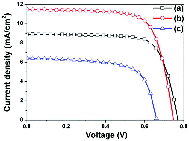 | ||
| Fig. 5 Current density–voltage curves of DSSCs with open-ended TiO2 nanotube arrays (a) without carbon doping and with carbon doping via CVD for (b) 30 s and (c) 60 s. | ||
| DSSCs based on open-ended TiO2 nanotube arrays | J sc (mA cm−2) | V oc (V) | ff | η (%) | Dye loading (nmol cm−2) |
|---|---|---|---|---|---|
| No carbon doping | 8.88 | 0.77 | 0.74 | 5.07 | 151 |
| Carbon doping for 30 s | 11.49 | 0.75 | 0.72 | 6.21 | 143 |
| Carbon doping for 60 s | 6.43 | 0.66 | 0.67 | 2.87 | 93 |
Fig. 6 shows the EIS spectra of DSSCs with and without carbon materials in open-ended TiO2 nanotube arrays across a frequency range from 10−2 to 106 Hz. The applied bias voltage and AC amplitude were set at the open circuit voltage (Voc) of the DSSCs and 10 mV, respectively. Each spectrum contains two semicircles: a small one at high frequency, and a large one at low frequency. The smaller semicircle is assigned to the parallel combination of the resistance and capacitance at the Pt–FTO/electrolyte and the FTO/TiO2 interfaces, and the larger semicircle is associated with the resistance and capacitance at the dye-absorbed TiO2/electrolyte interface and the transport resistance. The data were analyzed using an equivalent circuit, and the fit parameters are listed in Table 3. The Ohmic series resistance (Rs) is caused by the sheet resistance, and corresponds to the value of the x-axis where the first semicircle begins on the left-hand side. The values of Rs were similar with and without carbon doping on the TiO2 nanotube arrays, meaning that carbon doping did not affect the sheet resistance of FTO or the current collector. R1 is given by the sum of the interfacial resistances of FTO/TiO2 and Pt/electrolyte, while R2 is given by the sum of the charge transfer resistance at the dye-adsorbed TiO2/electrolyte interface and the transport resistance in the TiO2 films. DSSCs without carbon doping on the TiO2 nanotube arrays showed higher values of R1 (4.013 Ω) and R2 (34.05 Ω) than were found for DSSCs that had been carbon doped for 30 s, where R1 and R2 were 2.866 Ω and 27.73 Ω, respectively. This shows that a small amount of carbon decreases the resistance of TiO2 nanotube arrays due to π–π conjugation. Moreover, the π–π conjugation affects the conduction band of the TiO2 nanotube arrays, decreasing the Voc from 0.77 V to 0.75 V. As shown in Table 2, when carbon doping was performed for 60 s, the values of R1 (4.023 Ω) and R2 (47.55 Ω) were higher than in undoped DSSCs due to the lower dye loading level. The large amount of carbon materials on the TiO2 nanotube arrays disrupts the dye adsorption on the TiO2 nanotube arrays, meaning that charge cannot be generated. This increases the resistance at the dye-adsorbed TiO2/electrolyte interface and the transport resistance in the TiO2 films. As for the other doped material, the π–π conjugation affects the conduction band of the TiO2 nanotube arrays, greatly decreasing the Voc from 0.77 V to 0.66 V. The Voc is defined as the difference between the energy levels of the semiconductor and the electrolyte in a solar cell. When TiO2 nanotube arrays are doped with carbon, the conduction band edge of the TiO2 nanotube arrays shifts downward, which is referred to as “band bending”. For this reason, too much carbon doping can decrease the Voc.
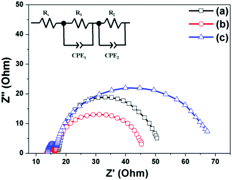 | ||
| Fig. 6 Impedance spectra of DSSCs with open-ended TiO2 nanotube arrays (a) without carbon doping and with carbon doping via CVD for (b) 30 s and (c) 60 s. | ||
| DSSCs based on open-ended TiO2 nanotube arrays | R s (Ω) | R 1 (Ω) | CPE1 (F) | R 2 (Ω) | CPE2 (F) |
|---|---|---|---|---|---|
| No carbon doping | 13.46 | 4.013 | 7.878 × 10⁻⁶ | 34.05 | 2.325 × 10⁻³ |
| Carbon doping for 30 s | 13.70 | 2.866 | 1.268 × 10⁻⁶ | 27.73 | 2.872 × 10⁻³ |
| Carbon doping for 60 s | 13.42 | 4.023 | 5.977 × 10⁻⁶ | 47.55 | 2.568 × 10⁻³ |
Conclusion
We synthesized carbon materials on closed- and open-ended TiO2 nanotube arrays for use in DSSCs in order to improve electron transport. The energy conversion efficiencies of DSSCs using TiO2 nanotube arrays that had been carbon doped for 30 s were better than those of cells using TiO2 that had not been carbon doped. However, the energy conversion efficiencies of DSSCs based on TiO2 nanotube arrays that had been carbon doped for 60 s were lower than the control cell. Based on the impedance data and the amount of dye adsorption, it can be seen that a smaller amount of carbon materials was more efficient in improving electron transport due to π–π conjugation of the carbon sp2 sites, while a large amount of carbon materials not only decreases dye adsorption on the TiO2 nanotube arrays but also decreases the ff of the DSSCs. We expect that our research can also be applied to photovoltaics such as perovskite solar cells, solid-state dye-sensitized solar cells, or hybrid solar cells.Acknowledgements
This research was supported by the Basic Science Research Program through the National Research Foundation of Korea (NRF) funded by the Ministry of Science, ICT & Future Planning (2016-A002-0048) and by the Bio & Medical Technology Development Program of the National Research Foundation (NRF) & funded by the Korean government (MSIP&MOHW) (2016-A423-0045).References
- B. Oregan and M. Gratzel, Nature, 1991, 353, 737–740 CrossRef CAS.
- S. Ito, T. N. Murakami, P. Comte, P. Liska, C. Gratzel, M. K. Nazeeruddin and M. Gratzel, Thin Solid Films, 2008, 516, 4613–4619 CrossRef CAS.
- M. Gratzel, Nature, 2001, 414, 338–344 CrossRef CAS PubMed.
- A. Ghicov, S. P. Albu, R. Hahn, D. Kim, T. Stergiopoulos, J. Kunze, C. A. Schiller, P. Falaras and P. Schmuki, Chem. – Asian J., 2009, 4, 520–525 CrossRef CAS PubMed.
- P. Roy, D. Kim, I. Paramasivam and P. Schmuki, Electrochem. Commun., 2009, 11, 1001–1004 CrossRef CAS.
- J. H. Park, T. W. Lee and M. G. Kang, Chem. Commun., 2008, 2867–2869 RSC.
- Q. W. Chen and D. S. Xu, J. Phys. Chem. C, 2009, 113, 6310–6314 CAS.
- C. J. Lin, W. Y. Yu and S. H. Chien, J. Mater. Chem., 2010, 20, 1073–1077 RSC.
- L. L. Li, Y. J. Chen, H. P. Wu, N. S. Wang and E. W. G. Diau, Energy Environ. Sci., 2011, 4, 3420–3425 CAS.
- C. Rho and J. S. Suh, Chem. Phys. Lett., 2011, 513, 108–111 CrossRef CAS.
- C. Rho, J. H. Min and J. S. Suh, J. Phys. Chem. C, 2012, 116, 7213–7218 CAS.
- C. M. Ruan, M. Paulose, O. K. Varghese, G. K. Mor and C. A. Grimes, J. Phys. Chem. B, 2005, 109, 15754–15759 CrossRef CAS PubMed.
- S. So, K. Lee and P. Schmuki, Chem. – Eur. J., 2013, 19, 2966–2970 CrossRef CAS PubMed.
- W.-Y. Rho, H. Jeon, H.-S. Kim, W.-J. Chung, J. S. Suh and B.-H. Jun, J. Nanomater., 2015, 247689 Search PubMed.
- J. M. Macak, H. Tsuchiya, A. Ghicov, K. Yasuda, R. Hahn, S. Bauer and P. Schmuki, Curr. Opin. Solid State Mater. Sci., 2007, 11, 3–18 CrossRef CAS.
- K. Shankar, G. K. Mor, H. E. Prakasam, S. Yoriya, M. Paulose, O. K. Varghese and C. A. Grimes, Nanotechnology, 2007, 18, 065707 CrossRef.
- G. K. Mor, O. K. Varghese, M. Paulose, K. Shankar and C. A. Grimes, Sol. Energy Mater. Sol. Cells, 2006, 90, 2011–2075 CrossRef CAS.
- J. Yan and F. Zhou, J. Mater. Chem., 2011, 21, 9406–9418 RSC.
- J. R. Jennings, A. Ghicov, L. M. Peter, P. Schmuki and A. B. Walker, J. Am. Chem. Soc., 2008, 130, 13364–13372 CrossRef CAS PubMed.
- S. Muduli, W. Lee, V. Dhas, S. Mujawar, M. Dubey, K. Vijayamohanan, S.-H. Han and S. Ogale, ACS Appl. Mater. Interfaces, 2009, 1, 2030–2035 CAS.
- J. Liu, Y.-T. Kuo, K. J. Klabunde, C. Rochford, J. Wu and J. Li, ACS Appl. Mater. Interfaces, 2009, 1, 1645–1649 CAS.
- S. R. Sun, L. Gao and Y. Q. Liu, Appl. Phys. Lett., 2010, 96, 3113 Search PubMed.
- Y. B. Tang, C. S. Lee, J. Xu, Z. T. Liu, Z. H. Chen, Z. B. He, Y. L. Cao, G. D. Yuan, H. S. Song, L. M. Chen, L. B. Luo, H. M. Cheng, W. J. Zhang, I. Bello and S. T. Lee, ACS Nano, 2010, 4, 3482–3488 CrossRef CAS PubMed.
- J. Yan, G. Wu, N. Guan, L. Li, Z. Li and X. Cao, Phys. Chem. Chem. Phys., 2013, 15, 10978–10988 RSC.
- W.-Y. Rho, M.-H. Chun, H.-S. Kim, Y.-B. Hahn, J. S. Suh and B.-H. Jun, Bull. Korean Chem. Soc., 2014, 35, 1165–1168 CrossRef CAS.
Footnotes |
| † Electronic supplementary information (ESI) available. See DOI: 10.1039/c6nj02615j |
| ‡ These authors contributed equally to the work. |
| This journal is © The Royal Society of Chemistry and the Centre National de la Recherche Scientifique 2017 |