
Non-conventional charge transport in organic semiconductors: magnetoresistance and thermoelectricity
Oliver
Fenwick
*ab and
Emanuele
Orgiu
 *c
*c
aSchool of Engineering and Materials Science, Queen Mary University of London Mile End Road, London E1 4NS, UK
bThe Organic Thermoelectrics Laboratory, Materials Research Institute, Queen Mary University of London Mile End Road, London E1 4NS, UK. E-mail: o.fenwick@qmul.ac.uk
cInstitut National de la recherche scientifique (INRS), EMT Center - 1650 Boul. Lionel Boulet, J3X 1S2 Varennes (QC), Canada. E-mail: emanuele.orgiu@emt.inrs.ca
First published on 4th January 2017
Abstract
High mobility charge transport in various organic semiconductors is now well documented and well understood. As a result, research is now focussing on more exotic transport properties driving a new generation of organic electronic devices. This mini-review will focus on the two most prominent of these, magnetoresistance and thermoelectricity. Each requires additional properties of materials beyond their ability to transport charge, namely a large resistive response to a magnetic field, or in the case of thermoelectrics a large Seebeck coefficient combined with low thermal conductivity. This mini-review will explore the current state of the art in organic materials for these applications and will discuss current ideas on the molecular and structural origins of their properties with an outlook on future directions for molecular design.
 Oliver Fenwick | Oliver Fenwick received his BA and MSci degrees from University of Cambridge (UK) and his PhD from University College London (UK). He worked on various aspects of organic electronics during post-doctoral positions at University College London and Université de Strasbourg (FR) before taking up his current position as a Royal Society University Research Fellow and Lecturer in Materials Science at Queen Mary University of London (UK). His group is focussed on developing organic thermoelectric materials and devices. |
 Emanuele Orgiu | Emanuele Orgiu received his M.S. (2004) and Ph.D. (2008) both from Università degli Studi di Cagliari (IT). He was awarded a Fulbright (USA) and Marie-Curie fellowship (FR) in 2007 and 2009, respectively. He became Assistant Professor in 2011 at the Université de Strasbourg (FR) where he was awarded the MIT35 France in 2013. Since 2016, he is also Associate Professor at INRS - EMT Center in Montreal (CA) where, along with his research team, he focuses on understanding novel electronic and optical phenomena occurring in molecular solids such as organic (semi)conductors or 2D materials such as graphene and transition metal dichalcogenides. |
Design, System, ApplicationThe research fields of organic magnetoresistance and thermoelectrics are relatively fresh but there is already a body of research which is beginning to unravel the underlying mechanisms in these materials. This work emphasizes the fact that a concerted synthetic effort is needed to renew molecular designs in order to create materials with functionalities that are tailored for applications in thermoelectricity and organic magnetoresistance. This will lead to new materials which will allow very fine magnetic field sensing and harvesting of heat loss. |
1. Organic magnetoresistance (OMAR) effects
1.1. Introduction to OMAR
In the past decade organic electronics crossed the path of the field of spintronics with increasing attention being focussed on spin physics and magnetic field effects in organic π-conjugated systems.1 More recently, large magnetic field effects were measured at room temperature in organic semiconductors with non-magnetic electrodes i.e. without any spin-injection into the active layer. These effects are known collectively as magnetoelectroluminescence and the magnetoresistance,2–6 which were initially reported in an organic light-emitting diode based on aluminium quinolone.7 The latter effect, described within this manuscript, sometimes referred to as organic magnetoresistance (OMAR) and defined as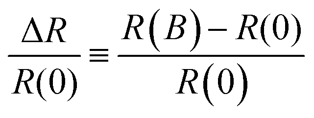 | (1) |
Several mechanisms have been suggested to explain OMAR9 including the electron–hole pair model,7,10,11 bipolaron model,2,4 triplet–polaron interaction model,12,13 and triplet–triplet annihilation model.14 Here we consider that the bipolaron formation4,15,16 represents the main source of OMAR and focus on molecular design principles related to this mechanism. Charge carrier interactions in organic semiconductors are mediated by vibrational fields, and the nature of such interactions is attractive even in charge pairs of the same sign, i.e. electron–electron or hole–hole. A charge along with its vibrational field forms a so-called “polaron”. Because of the large electron–phonon coupling, the polaron conduction in disordered materials occurs mostly via hopping between localized sites. As anticipated, it is possible, in principle, that two positively (hole) or negatively (electron) charged polarons share the same site. Coulomb repulsion opposes the formation of bipolarons (two small polarons localized either at the same lattice site or at two different but neighbouring lattice sites) which is favoured by electron–phonon–electron interaction. If the latter dominates the Coulomb repulsion, the two carriers can occupy the same site. The double occupancy of a lattice site leads to the formation of a bipolaron localized on the site. In addition, whether or not a bipolaron will be formed depends on the spin configuration of the each polaron: when two polarons meet, they possess a randomly oriented spin. A bipolaron can only form in the singlet (ground) state because of on-site exchange effects17 and a triplet state cannot be formed. When no external magnetic field (Bext) is applied (or when Bext is small compared to the hyperfine field, Bhf), the spin of each polaron sitting on a hydrocarbon molecule precesses about the (random) local magnetic field produced by the hydrogen nuclei, called the hyperfine field (Bhf). The random orientation of the Bhf associated with each polaron allows a transition to a spin-singlet bipolaron. Consider a pair of polarons, p1 and p2, possessing either (i) parallel and antiparallel initial spin (with respect to the local field) or (ii) both parallel initial spin states. In the absence of an external magnetic field, both initial spin states (i) and (ii) can lead to the formation of a spin-singlet bipolaron. This process is called spin-mixing and ensures that even a polaron pair that could potentially acquire a triplet character (therefore not forming a bipolaron) can still mix with a singlet character therefore allowing bipolaron formation (Fig. 1a). However, when an external magnetic field is applied (Bext ≫ Bhf) the spins of the two polarons on different sites can only precess about Bext, which will force the spins of p1 and p2 to be parallel. Hence, if p1 and p2 were in initial state (ii) a bipolaron could not be formed (Fig. 1b). The latter case describes a phenomenon of spin blockade, which makes that specific site no longer available for charge carriers, which will have to take another transport path. Spin blockade over a number of (molecular) sites will generate a decrease in the measured current which is associated to an increase in resistance upon the application of an external magnetic field larger than the hyperfine field. This is magnetoresistance with positive sign. In general, the sign is not always positive and it has been found to change as a function of voltage and temperature.2,18–20 The sign change in vertical devices with electroluminescent active layers has been ascribed to a different ratio between majority and minority charge carriers induced by the magnetic field which can cause a decrease (positive magnetoresistance) or an increase (negative magnetoresistance) in device current upon application of Bext.
 | ||
| Fig. 1 (a) No external magnetic field applied allows spin-mixing between two polarons thanks to spin precession; (b) when an external magnetic field Bext ≫ Bhf is applied, they both precess about Bext which prevents the formation of the bipolaron and of electrical conduction across that molecule. | ||
1.2. Molecular approaches to engineering OMAR
As introduced previously, the main mechanism proposed for explaining the OMAR effect relies on the fact that the bipolaron formation is magnetic field dependent.4,15,16 In the absence of an external magnetic field, the (hole) polaron formation rate follows the general trend:21,22 | (2) |
In a three-terminal device 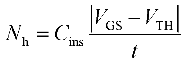 where Cins is the gate dielectric capacitance, t is the thickness of the conductive channel (1–3 nm) and VGS − VTH is the difference between gate-source and threshold voltage respectively. This simple expression reveals that the bipolaron concentration depends on the number of majority carriers involved in the transport which is set by the gate voltage (at a given drain-source voltage which ensures longitudinal electric field). We stress that the use of a three-terminal transistor device for testing bipolaron formation is key as it can induce a high and controllable charge carrier density within the semiconducting film. This allows one to monitor the formation rate of the bipolarons by varying the hole (electron) density. Street et al.22 found that a polyfluorene derivative, F8T2, and regioregular polythiophene both follow the proposed law (eqn (2)), but their propensity to form bipolarons, expressed by c, differed. This was ascribed to a different bipolaron binding energy and highlights the strong dependence of bipolaron formation on the specific material. This picture gets even clearer if one thinks of bipolarons as negative correlation states that should be stabilized through a relaxation of the polymer backbone as a consequence of the formation of a “two-polaron” bound state. The local polymer structure is strongly correlated to the relaxation energy which, again, points towards a dependence of the bipolaron formation on the material and its structural order. Generally speaking, organic polymer semiconductors are polycrystalline and disordered materials and, as a consequence, the degree of order of the film will dictate the local bipolaron concentration within the film as well as the physical location where the bipolaron formation can occur. Further investigations were carried out by the Vardeny group23 who observed polaron states with different energy in polythiophenes which were ascribed to the presence of an ordered and a disordered phase, respectively. Bipolaron formation is certainly favoured at specific sites within the film. Most likely, bipolarons are formed not in the crystalline portions of the film but rather at the grain boundaries or at the dielectric interface.
Another important observation on how to design polymers which feature high OMAR is given by Kersten et al.24 In this work, the role of energetic disorder, (intrinsic) dopant strength and interchain hopping is discussed for polymers. The first two are not found to significantly influence the OMAR whilst controlling inter- and intra-chain transport plays a key role. In particular, precise molecular design rules are provided such as: (i) reducing the coupling between each monomer unit in order to reduce the hopping vs. hyperfine precession rate; (ii) favouring 1D charge transport by reducing interchain hopping (Fig. 2).
 | ||
| Fig. 2 Relationship between magnetic field effect and ratio between interchain rate (kinterchain) and hopping rate (khop) in absence of disorder and at high electron density. Reproduced with permission from ref. 24 Copyright. | ||
An interesting example of experimental engineering of the (radiative) charge traps within the active layer of the device and their role on OMAR was explored by Cox et al.25 The authors conceived an experiment where the magnetic field effects measured in several co-polymers were also monitored by optical spectroscopy. The co-polymers were built by combining different polymer units, each one possessing distinct emission properties which allowed direct spectroscopic monitoring of the related magnetic phenomena. Their findings confirmed that spin mixing at the trap sites is responsible for the large OMAR effects observed experimentally.
Furthermore, the role of the dielectric/semiconductor and metal/semiconductor interfaces on OMAR is also rather unexplored. While organic semiconductors can be considered as van der Waals molecular solids, where the molecular interactions are rather weak, this character has strong repercussions on their structural and energetic order which is much lower compared to their inorganic counterparts. The dependence of charge transport and injection on the interfaces presents a challenge but can be turned into an advantage for tuning the OMAR effect. It is widely accepted that in organic field-effect transistors charges move near to the semiconductor/dielectric interface and hence control over possible structural and energetic disorder at the interface is of paramount importance.26 For instance, it has been shown by several studies that high-k dielectrics influence the distribution of the DOS by creating dipolar disorder at the interface with the semiconductor.27,28 More precisely, the dipolar disorder generates a broadening of the DOS. The broadening is mostly due to energy fluctuations generated by local and randomly oriented dipoles. We believe this is an important parameter affecting the bipolaron formation since it is intimately related to the width of the DOS. When such width is large, charge carriers will experience a higher hopping barrier which will increase the magnetoresistance and lead to higher local concentrations of bipolarons with respect to the case where low-k dielectrics are used.
Molecular engineering of the metal/semiconductor interface certainly represents a powerful tool to control OMAR. As an example, it has been widely reported in literature that various physical and chemical properties such as the metal work function can be adjusted by using various self-assembled monolayers (SAMs) chemisorbed on metal electrodes.29,30 Surface modifications of metal electrodes via SAMs are typically done to achieve energetic alignment between the metal work function, Φm, and the HOMO (LUMO) level of the organic semiconductor or at least to reduce the charge injection barrier at such interface. Interfacial morphology and tunnelling resistance associated to the SAM have also been found to strongly influence the charge injection as has been reported for alkanethiol-coated electrodes.31 A recent study20 reported on the effect of the insertion of a fluoro-SAM functionalized gold electrode on the associated magnetoresistance. Interestingly, the authors found that a central role was played by the change in interfacial morphology due to the change in wettability upon chemisorption of the SAM (Fig. 3). Furthermore, insertion of the fluoro-SAM led to the intriguing discovery that the sign of the OMAR could change. Whilst this further underlines the significant impact of morphology and structural order of the semiconductor on the magnetoresistance, the effect of a strong interfacial molecular dipole (which led to an increase in the measured work-function) could not be disentangled from the morphological effects and this and other aspects will certainly need to be analysed more in depth in the near future.
 | ||
Fig. 3 (Top panel) Schematic layout of the Au/TPD/Alq3/Ca device that includes a Au bottom electrode functionalised with fluorinated self-assembled monolayers (F-SAM). (Bottom panel) Magnetoresistance variation vs. in-plane magnetic field of the with (right) and without (left) F-SAM treatment on Au. The measurements were realized at room temperature with a bias voltage of 3.0 and 8.0 V (black lines). The data were fitted with a combined model of empirical non-Lorentzian and  dependence (red lines). Reproduced with permission from ref. 20 Copyright. dependence (red lines). Reproduced with permission from ref. 20 Copyright. | ||
2. Organic thermoelectric materials
2.1. Overview of organic thermoelectrics
A thermoelectric device typically consists of two thermoelectric materials, one p-type and one n-type semiconductor, sandwiched between a hot electrode (T = Th) and a cold one (T = Tc) as schematised in Fig. 4a. Greater thermal motion of charge carriers at the hot side compared to the cold leads to a charge density gradient which opposes the temperature gradient. This can be detected as a thermal voltage, ΔV, across the two sides of the material whose magnitude is governed by the material's Seebeck coefficient, S = ΔV/ΔT, and allows useful electrical power to be extracted. | ||
| Fig. 4 a Schematic of a planar printed thermoelectric device (left) incorporating a p-type hybrid polymer–inorganic material (Te-PEDOT:PSS). The n-type legs are substituted with silver. The printed device is shown on the right. Reproduced from Bae et al.74 with permission. b A wearable microstructure-frame-supported organic thermoelectric device able to detect temperature and pressure changes (left). Temperature map (right) detected from the same device. Reproduced from Zhang et al.113 with permission. | ||
The maximum efficiency, ηTE, of any thermoelectric device can be written as a function of the Carnot efficiency, ηc = (Th − Tc)/Th.
 | (3) |
| ZT = σS2T/κ | (4) |
A good thermoelectric material must therefore possess a high electrical conductivity combined with a large Seebeck coefficient and a low thermal conductivity. ZT ≥ 1 is generally considered necessary for most applications. The great challenge of developing improved organic thermoelectric materials is the strong interdependence between the three thermoelectric properties σ, S and κ, with optimisation of any one property having a detrimental effect on at least one of the others. In what follows, some of the strategies material development are discussed. It should be noted that eqn (3) only holds for small (Th − Tc), i.e. small enough that S is constant over the range Tc < T < Th and therefore that the Thomson effect is not significant, otherwise an integral form of eqn (3) should be adopted.32
Organic materials whose thermoelectric properties have been studied33 include polymers such as poly(thienothiophene),34 poly(ethylene-dioxythiophene)35–41 (PEDOT), polyaniline,42 poly(p-phenylene vinylene) derivatives,43,44 poly(3-hexylthiophene),45,46 carbazole polymers,47–49 metal coordination polymers,50 and P(NDIOD-T2),51 as well as small molecules such as fullerenes,52–55 perylene diimide derivatives and organic salts based on TTF, TCNQ, BEDT-TTF and tetrathiotetracene amongst others.35,56–62 Of these, PEDOT has recently shown excellent performance as a p-type thermoelectric material with ZT reported up to 0.42.63 On the other hand, there has not been so much success in finding good n-type organic thermoelectric materials. Nonetheless ZT of up to 0.3 has been observed for poly(metal 1,1,2,2-ethenetetrathiolates)50,64 with reasonable power factors (σS2) of >400 μW m−1 K−2.64
2.2. Doping of organic thermoelectric materials
The conductivity of a material, σ, is proportional to the charge carrier mobility in that material, μ, and the carrier concentration, N:| σ = eNμ | (5) |
Thermoelectric materials are therefore metals or doped semiconductors and for most organic thermoelectric materials this means combining a high mobility intrinsic organic semiconductor with a suitable dopant, though there are also a few examples of organic thermoelectric materials which derive their conductivity through self-doping.50,65,66 Doped polymer films can be produced with conductivities >3000 S cm−1.67
Choosing a suitable dopant requires consideration of its oxidation or reduction potential relative to the transport level of the semiconductor, the doping efficiency in the target semiconductor and the degree of doping required. Atomic and small molecule dopants such as lithium, strontium, iodine, bromine or certain Lewis acids are sometimes used44,68–71 but are often not ideal for devices as they can diffuse at moderate temperatures and reduce operating lifetimes.72 Molecular dopants are usually preferable as they are less mobile in the solid state.
P-type molecular dopants include 7,7,8,8-tetracyanoquinodimethane (TCNQ), 2,3,5,6-tetrafluoro-7,7,8,8-tetracyanoquinodimethane (F4-TCNQ),73 tosylate (Tos),35,41 poly(styrenesulfonate)40,74 (PSS) and chloranil75 amongst others. Since an n-type molecular dopant must possess a HOMO above the LUMO of the semiconductor they are typically less chemically stable and the options are much reduced. Examples are dihydro-1H-benzoimidazol-2-yl (N-DBI),51 bis(ethylenedithio)-tetrathiafulvalene (BEDT-TTF),76 tetrathianaphthacene (TTN),77 bis(cyclopentadienyl)-cobalt(II) (cobaltocene, CoCp2)78 and dimetal complexes.53,79,80 Alkali metals may also be used, but with the limitations on device lifetime noted above. A way around chemical or device stability issues is to use air-stable dopant precursors that dope through an intermediate state as is the case for rhodocene dimers81 and some cationic dyes.82,83
Since increasing the conductivity can decrease the Seebeck coefficient and increase the thermal conductivity (vide infra), optimum doping levels for thermoelectric applications are typically a little lower than for solely high conductivity applications. In the case of PEDOT: PSS or PEDOT:Tos, for example, acido-basic control of conductivity41,74 can be achieved by immersion of the pre-deposited films in acidic or basic solutions can be used to de-dope the as-synthesised material to maximise ZT. A number of post-deposition solvent treatments are also available which can boost conductivity and ZT such as rinsing with (di)ethylene glycol, DMF, H2SO4 or DMSO.40,63,74,84
Typical charge carrier concentrations in optimised thermoelectric materials are ∼1018–1020 per cm3.37,74 Introducing the required quantity of dopants will have an impact on the packing and geometry of the semiconductor. Furthermore, the dopants increase ionised impurity scattering37 and can cause a broadening of the density of states in the semiconductor.73 It is therefore a complex challenge to increase N without reducing μ. Nonetheless, this is possible in PEDOT due to the aromatic to quinoid transition at high doping levels. The quinoid form is more planar which allows a higher degree of crystallinity and shorter π-stacking distances37,84 but for many materials μ decreases with increasing doping.
It is important to ensure a high doping efficiency to reduce number of dopants to achieve the desired N. This is determined partly by oxidation/reduction potentials of the dopant relative to the transport level of the semiconductor, but also by the geometrical configuration of the dopant-semiconductor system.85 In certain donor–acceptor copolymers, the p-dopant F4-TCNQ located in the vicinity of the acceptor units contribute little to charge transfer compared to when it is located over acceptor units.86,87 Further factors which may limit the doping efficiency include phase segregation of the dopants,51,87 the degree of delocalisation of the dopant-induced charge on the molecule/polymer86 and changes to the energy landscape caused either by frontier orbital hybridisation between the dopant and semiconductor37 or by ion-induced density of states broadening.73 To take an example, charge transfer between F4-TCNQ and P3HT is very efficient (up to 100%).73 However, the associated free charge density is very low, perhaps just 5% of the dopant density, with the remaining charges being Coulombically bound to the F4-TCNQ anion. Much higher (free charge) doping efficiencies (∼90%) are observed for PEDOT:Tos.37
An alternative approach to study molecular thermoelectric materials under high levels of doping is to use organic field effect transistors45 (OFETs) or electrochemically gated organic field-effect transistors38,45 (EG-OFET). This approach has the advantages of controlled gate modulation of the charge carrier density over orders of magnitude and the possibility of high doping levels (nearly 50% of the monomer density for EG-OFETS38) without altering the film morphology, though it is not a suitable architecture for a thermoelectric generator. In fact, with this approach, large power factors (σS2) are reported for the polymers PBTTT and P3HT45 that match or exceed those obtained for PEDOT EG-OFETs.38 This result strongly suggests that accurate control morphology whilst doping may open up the range of organic thermoelectric materials exhibiting ZT > 0.1.
2.3. Molecular control over the Seebeck coefficient
Engineering of the Seebeck coefficient, S, in organic thermoelectric materials has not been so extensively explored. Here we will highlight some key relations and discuss how these relate to S in organic materials. For intrinsic semiconductors, S is linked to the difference in energy between the Fermi level, EF, and the transport level, Etrans, by the Boltzmann equation: | (6) |
For heavily doped systems, where EF ≈ Etrans, a can become significant. This is the case for many organic thermoelectric materials, including PEDOT which can be considered a semi-metal under certain conditions.84 In this regime, the Boltzman equation reduces to the Mott relationship:88,89
 | (7) |
Importantly it can be seen that S is maximised by a sharp increase in the density of states around the Fermi level. For metals as well as highly oxidized polyaniline42 the Fermi level lies in the middle of the band and they therefore have low thermopower. An S ∝ ln![[thin space (1/6-em)]](https://www.rsc.org/images/entities/char_2009.gif) σ relationship is commonly observed for polymers including polyaniline,42 and P3HT46 (Fig. 5a).
σ relationship is commonly observed for polymers including polyaniline,42 and P3HT46 (Fig. 5a).
 | ||
| Fig. 5 a Conductivity plotted against Seebeck coefficient for P3HT films, showing the typical S ∝ lnσ relationship. Reproduced from Xuan et al.46 with permission. b In-plane thermal conductivity plotted against electrical conductivity for DMSO-mixed PEDOT:PSS. Adapted from Liu et al.105 with permission. | ||
Improved order in a polymer film is one way to boost σ without decreasing S. For example, the S ∝ lnσ relationship is maintained in polyaniline films upon doping, yet stretching the films to align the polymer can boost σ at a fixed S.42 This emerges from a reduction in localised energy levels near EF that tend to smooth out the density of states. A similar effect can also be achieved in PEDOT by using a number of solvent additives which improve ordering in resultant films.84 Counterintuitively, the Seebeck coefficient in PEDOT:ToS films has been shown to increase with conductivity. This remarkable result is attributed to its bipolaronic band structure with an empty bipolaron band merging into the valence band. This semi-metallic electronic structure possesses a rapidly varying density of states at the Fermi level which is highly sensitive to structural order and allows the increase of Seebeck coefficient with increasing conductivity.
Although eqn (6) and (7) do hold for hopping transport,90 the complexities of organic semiconductors require a more complete theory for S. One approach is to remove the assumption of discrete energy levels and build a broader Gaussian distribution of the density of states into the model,91 which can additionally include the effects of charge trapping.92 Disorder in organic semiconductors manifests itself in a wide variety of temperature dependencies of S. S can increase or decrease with temperature depending on the wave-function overlap for carriers of a particular energy.93 In fact, the work of Sirringhaus et al.94 and Zuppiroli et al.95 points to temperature independent Seebeck coefficients for systems where the energetic disorder of the transport level is minimised (IDTBT94 and single crystal pentacene95). The case of the polymer IDTBT has a particularly interesting chemical design where the energetic order is relatively unaffected by structural disorder.
To this point we have only considered electronic transport, yet the charge carriers in organic semiconductors are polarons. The lattice distortion of the polaron gives rise to a self-energy which will modify the hopping rate with the overall effect of a decrease in S that is dependent on the magnitude of the self-energy.96 It should also be noted that the geometry used for measurement of S also has a strong influence. For example, in organic field effect transistor the current flows in a very thin zone close to the dielectric interface, and surface dipoles at this interface can play a significant role in modifying the density of states97 and consequently have a strong effect on S.98 In chemically doped materials there will certainly be an effect on S from ionised dopants. Whilst it can be challenging to anticipate S in organic semiconductors, its sensitivity to a range of factors makes it a very useful tool to understand charge transport in thermoelectric materials.
2.4. Controlling thermal conductivity
Inorganic thermoelectric materials suffer in most cases from high thermal conductivity which often has to be reduced by nanostructuring to introduce interfaces (grain boundaries or inclusions) which scatter phonons more strongly than electrons.99,100 Intrinsic organic semiconductors exhibit low thermal conductivities of κ ≈ 0.1–1 W mK−1 (ref. 35 and 101) which are equal to or lower than most state-of-the-art nanostructured inorganic materials. Due to this intrinsically low thermal conductivity, efforts to engineer high ZT organic materials have mostly focussed on improving σ and S. Nonetheless, κ remains important and a deeper understanding is required to establish whether organic thermoelectric materials can achieve, for example, the ultra-low thermal conductivities of certain fullerenes such as PCBM (0.03–0.05 W mK−1).102–104Thermal conductivity, κ comprises lattice and electronic contributions, κL and κE respectively, where κ = κL + κE. The electronic component is intimately linked to the electrical conductivity, σ, by the Wiedemann–Franz law, κE = σLT, where L is the Lorentz number. Therefore, reducing thermal conductivity in thermoelectric materials must focus on minimising κL and the Lorentz number, L. The value of κL is linked to phonon scattering and is decreased by grain boundaries and disorder, by designing molecules whose composite atoms span a wide range of atomic weights, or by including loosely bound atoms in the structure (so-called rattling modes). An example of the latter are the poly(metal 1,1,2,2-ethenetetrathiolate)s50 which exhibit a modest thermal conductivity over a wide temperature range.
L has been measured for PEDOT:PSS105,106 and PEDOT:Tos.106 The validity of the Wiedemann–Franz law was verified, but there is still debate over the value of L, with two reports105,107 suggesting L is equal to the Sommerfeld value for a free electron gas, Ls = 2.45 × 10⁻⁸ W Ω K−2,108 and another two106,109 finding different values of L. On top of this, theoretical work further suggests L < Ls for low/intermediate doping concentrations in PEDOT:Tos.37 Charge transport in organic materials involves polarons and in polymers involves quasi-1-dimensional along-chain transport106 and therefore it should not be assumed that the Sommerfeld value must apply. The impact of the value of L on ZT is significant: κ increases by a factor of up to 3 between intrinsic PEDOT and PEDOT doped to levels typical for thermoelectric applications.105,106 How one might engineer L by molecular design is not yet clear, but perhaps some lessons should be learned from the inorganic community where it is known that the Lorenz number can be decreased by reducing the bandwidth of the charge carrier dispersion110 and can be tuned by nanostructuring.111,112
3. Outlook
Organic thermoelectric materials have been incorporated into flexible prototype devices either as conventional or planar thermoelectric generators74 or as thermal sensors.113 However, improvements in materials design are still needed to boost output powers and efficiencies of thermoelectric generators. There are a number of organic materials with charge carrier mobilities greater than PEDOT94,114–118 which gives us hope that the necessary improvements in ZT are within reach. This is especially true for n-type organic materials which are currently under-performing in thermoelectrics, which places limits on the performance of all-organic thermoelectric generators. By combining improved materials with improved processing focussing on molecular (polymer) alignment,42,119 morphology and hybrid composites36,74,120 there is a great potential for efficient organic thermoelectric generators in the near future. Analogously, a rigorous material design is needed for controlling spin mixing rules and therefore achieving control over magnetoresistance. In this regard, 1D wires minimizing the interchain hopping would be the most suitable structure to achieve such goal. This represents an important design rule for the materials which would be counterintuitive for attaining good charge transport. It is important that synthetic chemists in these fields focus on new design rules specific to magnetoresistance and thermoelectricity rather than on legacy design rules for charge transport materials.Furthermore, a number of doping strategies are yet be explored for controlling the thermoelectric and magnetoresistive properties of the films. The doping can be either substitutional (addition of molecular units to a given polymer chain/molecule) or interstitial (by blending with a second material).
In conclusion, the research fields of organic magnetoresistance and thermoelectrics are relatively fresh but there is already a body of research which is beginning to unravel the underlying mechanisms in these materials. This work emphasizes the fact that a concerted synthetic effort is needed to develop a new generation of materials with a more tailored molecular design.
Acknowledgements
OF is a Royal Society University Research Fellow.References
- V. A. Dediu, L. E. Hueso, I. Bergenti and C. Taliani, Nat. Mater., 2009, 8, 707–716 CrossRef CAS PubMed.
- O. Mermer, G. Veeraraghavan, T. L. Francis, Y. Sheng, D. T. Nguyen, M. Wohlgenannt, A. Kohler, M. K. Al-Suti and M. S. Khan, Phys. Rev. B: Condens. Matter Mater. Phys., 2005, 72, 205202 CrossRef.
- B. Hu, L. A. Yan and M. Shao, Adv. Mater., 2009, 21, 1500–1516 CrossRef CAS.
- P. A. Bobbert, T. D. Nguyen, F. W. A. van Oost, B. Koopmans and M. Wohlgenannt, Phys. Rev. Lett., 2007, 99, 216801 CrossRef CAS PubMed.
- V. N. Prigodin, J. D. Bergeson, D. M. Lincoln and A. J. Epstein, Synth. Met., 2006, 156, 757–761 CrossRef CAS.
- M. Wohlgenannt, Phys. Status Solidi RRL, 2012, 6, 229–242 CrossRef CAS.
- J. Kalinowski, M. Cocchi, D. Virgili, P. Di Marco and V. Fattori, Chem. Phys. Lett., 2003, 380, 710–715 CrossRef CAS.
- Y. F. Wang, K. Sahin-Tiras, N. J. Harmon, M. Wohlgenannt and M. E. Flatte, Phys. Rev. X, 2016, 6, 011011 Search PubMed.
- P. Janssen, M. Cox, S. H. W. Wouters, M. Kemerink, M. M. Wienk and B. Koopmans, Nat. Commun., 2013, 4, 2286 CAS.
- S. A. Bagnich, U. Niedermeier, C. Melzer, W. Sarfert and H. von Seggern, J. Appl. Phys., 2009, 105, 123706 CrossRef.
- S. A. Bagnich, U. Niedermeier, C. Melzer, W. Sarfert and H. von Seggern, J. Appl. Phys., 2009, 106, 113702 CrossRef.
- P. Desai, P. Shakya, T. Kreouzis, W. P. Gillin, N. A. Morley and M. R. J. Gibbs, Phys. Rev. B: Condens. Matter Mater. Phys., 2007, 75, 094423 CrossRef.
- P. Desai, P. Shakya, T. Kreouzis and W. P. Gillin, Phys. Rev. B: Condens. Matter Mater. Phys., 2007, 76, 235202 CrossRef.
- A. H. Davis and K. Bussmann, J. Vac. Sci. Technol., A, 2004, 22, 1885–1891 CAS.
- A. J. Schellekens, W. Wagemans, S. P. Kersten, P. A. Bobbert and B. Koopmans, Phys. Rev. B: Condens. Matter Mater. Phys., 2011, 84, 075204 CrossRef.
- J. Danon, X. H. Wang and A. Manchon, Phys. Rev. Lett., 2013, 111, 066802 CrossRef PubMed.
- M. N. Bussac and L. Zuppiroli, Phys. Rev. B: Condens. Matter Mater. Phys., 1993, 47, 5493 CrossRef CAS.
- F. L. Bloom, M. Kemerink, W. Wagemans and B. Koopmans, Phys. Rev. Lett., 2009, 103, 066601 CrossRef CAS PubMed.
- F. L. Bloom, W. Wagemans and B. Koopmans, J. Appl. Phys., 2008, 103, 07F320 CrossRef.
- H. J. Jang, S. J. Pookpanratana, A. N. Brigeman, R. J. Kline, J. I. Basham, D. J. Gundlach, C. A. Hacker, O. A. Kirillov, O. D. Jurchescu and C. A. Richter, ACS Nano, 2014, 8, 7192–7201 CrossRef CAS PubMed.
- A. Salleo and R. A. Street, Phys. Rev. B: Condens. Matter Mater. Phys., 2004, 70, 235324 CrossRef.
- R. A. Street, A. Salleo and M. L. Chabinyc, Phys. Rev. B: Condens. Matter Mater. Phys., 2003, 68, 085316 CrossRef.
- X. M. Jiang, R. Österbacka, O. Korovyanko, C. P. An, B. Horovitz, R. A. J. Janssen and Z. V. Vardeny, Adv. Funct. Mater., 2002, 12, 587–597 CrossRef CAS.
- S. P. Kersten, S. C. J. Meskers and P. A. Bobbert, Phys. Rev. B: Condens. Matter Mater. Phys., 2012, 045210 CrossRef.
- M. Cox, M. H. A. Wijnen, G. A. H. Wetzelaer, M. Kemerink, P. W. M. Blom and B. Koopmans, Phys. Rev. B: Condens. Matter Mater. Phys., 2014, 90, 155205 CrossRef.
- F. Dinelli, M. Murgia, P. Levy, M. Cavallini, F. Biscarini and D. M. de Leeuw, Phys. Rev. Lett., 2004, 92, 116802 CrossRef PubMed.
- J. Veres, S. D. Ogier, S. W. Leeming, D. C. Cupertino and S. M. Khaffaf, Adv. Funct. Mater., 2003, 13, 199–204 CrossRef CAS.
- I. N. Hulea, S. Fratini, H. Xie, C. L. Mulder, N. N. Iossad, G. Rastelli, S. Ciuchi and A. F. Morpurgo, Nat. Mater., 2006, 5, 982–986 CrossRef CAS PubMed.
- I. H. Campbell, S. Rubin, T. A. Zawodzinski, J. D. Kress, R. L. Martin, D. L. Smith, N. N. Barashkov and J. P. Ferraris, Phys. Rev. B: Condens. Matter Mater. Phys., 1996, 54, 14321–14324 CrossRef.
- B. de Boer, A. Hadipour, M. M. Mandoc, T. van Woudenbergh and P. W. M. Blom, Adv. Mater., 2005, 17, 621–625 CrossRef CAS.
- P. Stoliar, R. Kshirsagar, M. Massi, P. Annibale, C. Albonetti, D. M. de Leeuw and F. Biscarini, J. Am. Chem. Soc., 2007, 129, 6477–6484 CrossRef CAS PubMed.
- H. S. Kim, W. Liu, G. Chen, C.-W. Chu and Z. Ren, Proc. Natl. Acad. Sci. U. S. A., 2015, 112, 8205–8210 CrossRef CAS PubMed.
- P. J. Taroni, I. Hoces, N. Stingelin, M. Heeney and E. Bilotti, Isr. J. Chem., 2014, 54, 534–552 CrossRef CAS.
- R. Yue, S. Chen, B. Lu, C. Liu and J. Xu, J. Solid State Electrochem., 2011, 15, 539–548 CrossRef CAS.
- O. Bubnova, Z. U. Khan, A. Malti, S. Braun, M. Fahlman, M. Berggren and X. Crispin, Nat. Mater., 2011, 10, 429–433 CrossRef CAS PubMed.
- K. Wei, T. Stedman, Z. H. Ge, L. M. Woods and G. S. Nolas, Appl. Phys. Lett., 2015, 107, 153301 CrossRef.
- W. Shi, T. Zhao, J. Xi, D. Wang and Z. Shuai, J. Am. Chem. Soc., 2015, 137, 12929–12938 CrossRef CAS PubMed.
- O. Bubnova, M. Berggren and X. Crispin, J. Am. Chem. Soc., 2012, 134, 16456–16459 CrossRef CAS PubMed.
- C. Liu, B. Lu, J. Yan, J. Xu, R. Yue, Z. Zhu, S. Zhou, X. Hu, Z. Zhang and P. Chen, Synth. Met., 2010, 160, 2481–2485 CrossRef CAS.
- E. Liu, C. Liu, Z. Zhu, H. Shi, Q. Jiang, F. Jiang, J. Xu, J. Xiong and Y. Hu, J. Polym. Res., 2015, 22, 1–5 CrossRef CAS.
- Z. U. Khan, O. Bubnova, M. J. Jafari, R. Brooke, X. Liu, R. Gabrielsson, T. Ederth, D. R. Evans, J. W. Andreasen, M. Fahlman and X. Crispin, J. Mater. Chem. C, 2015, 3, 10616–10623 RSC.
- N. Mateeva, H. Niculescu, J. Schlenoff and L. R. Testardi, J. Appl. Phys., 1998, 83, 3111–3117 CrossRef CAS.
- Y. Hiroshige, M. Ookawa and N. Toshima, Synth. Met., 2007, 157, 467–474 CrossRef CAS.
- Y. Hiroshige, M. Ookawa and N. Toshima, Synth. Met., 2006, 156, 1341–1347 CrossRef CAS.
- F. Zhang, Y. Zang, D. Huang, C.-a. Di, X. Gao, H. Sirringhaus and D. Zhu, Adv. Funct. Mater., 2015, 25, 3004–3012 CrossRef CAS.
- Y. Xuan, X. Liu, S. Desbief, P. Leclère, M. Fahlman, R. Lazzaroni, M. Berggren, J. Cornil, D. Emin and X. Crispin, Phys. Rev. B: Condens. Matter Mater. Phys., 2010, 82, 115454 CrossRef.
- R. B. Aïch, N. Blouin, A. Bouchard and M. Leclerc, Chem. Mater., 2009, 21, 751–757 CrossRef.
- I. Lévesque, P.-O. Bertrand, N. Blouin, M. Leclerc, S. Zecchin, G. Zotti, C. I. Ratcliffe, D. D. Klug, X. Gao, F. Gao and J. S. Tse, Chem. Mater., 2007, 19, 2128–2138 CrossRef.
- I. Lévesque, X. Gao, D. D. Klug, J. S. Tse, C. I. Ratcliffe and M. Leclerc, React. Funct. Polym., 2005, 65, 23–36 CrossRef.
- Y. Sun, P. Sheng, C. Di, F. Jiao, W. Xu, D. Qiu and D. Zhu, Adv. Mater., 2012, 24, 932–937 CrossRef CAS PubMed.
- R. A. Schlitz, F. G. Brunetti, A. M. Glaudell, P. L. Miller, M. A. Brady, C. J. Takacs, C. J. Hawker and M. L. Chabinyc, Adv. Mater., 2014, 26, 2825–2830 CrossRef CAS PubMed.
- Z. H. Wang, K. Ichimura, M. S. Dresselhaus, G. Dresselhaus, W. T. Lee, K. A. Wang and P. C. Eklund, Phys. Rev. B: Condens. Matter Mater. Phys., 1993, 48, 10657–10660 CrossRef.
- T. Menke, D. Ray, J. Meiss, K. Leo and M. Riede, Appl. Phys. Lett., 2012, 100, 093304 CrossRef.
- M. Sumino, K. Harada, M. Ikeda, S. Tanaka, K. Miyazaki and C. Adachi, Appl. Phys. Lett., 2011, 99, 093308 CrossRef.
- L. Rincon-Garcia, A. K. Ismael, C. Evangeli, I. Grace, G. Rubio-Bollinger, K. Porfyrakis, N. Agrait and C. J. Lambert, Nat. Mater., 2016, 15, 289–293 CrossRef CAS PubMed.
- W. Jens and P.-K. Karin, J. Phys. D: Appl. Phys., 2008, 41, 135113 CrossRef.
- E. A. Perez-Albuerne, H. Johnson and D. J. Trevoy, J. Chem. Phys., 1971, 55, 1547–1554 CrossRef CAS.
- J. W. Bray, H. R. Hart, L. V. Interrante, I. S. Jacobs, J. S. Kasper, P. A. Piacente and G. D. Watkins, Phys. Rev. B: Condens. Matter Mater. Phys., 1977, 16, 1359–1364 CrossRef CAS.
- M. G. Miles and J. D. Wilson, Inorg. Chem., 1975, 14, 2357–2360 CrossRef CAS.
- A. Casian and I. Sanduleac, J. Electron. Mater., 2014, 43, 3740–3745 CrossRef CAS.
- L. C. Isett, Phys. Rev. B: Condens. Matter Mater. Phys., 1978, 18, 439–447 CrossRef CAS.
- A. Casian and I. Sanduleac, Mater. Today, 2015, 2, 504–509 CrossRef.
- G. H. Kim, L. Shao, K. Zhang and K. P. Pipe, Nat. Mater., 2013, 12, 719–723 CrossRef CAS PubMed.
- Y. Sun, L. Qiu, L. Tang, H. Geng, H. Wang, F. Zhang, D. Huang, W. Xu, P. Yue, Y.-s. Guan, F. Jiao, Y. Sun, D. Tang, C.-a. Di, Y. Yi and D. Zhu, Adv. Mater., 2016, 28, 3351–3358 CrossRef CAS PubMed.
- B. Russ, M. J. Robb, F. G. Brunetti, P. L. Miller, E. E. Perry, S. N. Patel, V. Ho, W. B. Chang, J. J. Urban, M. L. Chabinyc, C. J. Hawker and R. A. Segalman, Adv. Mater., 2014, 26, 3473–3477 CrossRef CAS PubMed.
- C.-K. Mai, R. A. Schlitz, G. M. Su, D. Spitzer, X. Wang, S. L. Fronk, D. G. Cahill, M. L. Chabinyc and G. C. Bazan, J. Am. Chem. Soc., 2014, 136, 13478–13481 CrossRef CAS PubMed.
- M. V. Fabretto, D. R. Evans, M. Mueller, K. Zuber, P. Hojati-Talemi, R. D. Short, G. G. Wallace and P. J. Murphy, Chem. Mater., 2012, 24, 3998–4003 CrossRef CAS.
- J. Puigmartí-Luis, V. Laukhin, Á. Pérez del Pino, J. Vidal-Gancedo, C. Rovira, E. Laukhina and D. B. Amabilino, Angew. Chem., Int. Ed., 2007, 46, 238–241 CrossRef PubMed.
- G. Parthasarathy, C. Shen, A. Kahn and S. R. Forrest, J. Appl. Phys., 2001, 89, 4986–4992 CrossRef CAS.
- J. Kido and T. Matsumoto, Appl. Phys. Lett., 1998, 73, 2866–2868 CrossRef CAS.
- E. Jun, M. Toshio and K. Junji, Jpn. J. Appl. Phys., 2002, 41, L358 CrossRef.
- B. Lüssem, M. Riede and K. Leo, Phys. Status Solidi A, 2013, 210, 9–43 CrossRef.
- P. Pingel and D. Neher, Phys. Rev. B: Condens. Matter Mater. Phys., 2013, 87, 115209 CrossRef.
- E. J. Bae, Y. H. Kang, K.-S. Jang and S. Y. Cho, Sci. Rep., 2016, 6, 18805 CrossRef CAS PubMed.
- D. R. Kearns, G. Tollin and M. Calvin, J. Chem. Phys., 1960, 32, 1020–1025 CrossRef CAS.
- A. Nollau, M. Pfeiffer, T. Fritz and K. Leo, J. Appl. Phys., 2000, 87, 4340–4343 CrossRef CAS.
- T. Senku, K. Kaname, K. Eiji, I. Takashi, N. Toshio, O. Yukio and S. Kazuhiko, Jpn. J. Appl. Phys., 2005, 44, 3760 CrossRef.
- C. K. Chan, F. Amy, Q. Zhang, S. Barlow, S. Marder and A. Kahn, Chem. Phys. Lett., 2006, 431, 67–71 CrossRef CAS.
- F. A. Cotton, N. E. Gruhn, J. Gu, P. Huang, D. L. Lichtenberger, C. A. Murillo, L. O. Van Dorn and C. C. Wilkinson, Science, 2002, 298, 1971–1974 CrossRef CAS PubMed.
- F. A. Cotton, J. P. Donahue, D. L. Lichtenberger, C. A. Murillo and D. Villagrán, J. Am. Chem. Soc., 2005, 127, 10808–10809 CrossRef CAS PubMed.
- S. Guo, S. B. Kim, S. K. Mohapatra, Y. Qi, T. Sajoto, A. Kahn, S. R. Marder and S. Barlow, Adv. Mater., 2012, 24, 699–703 CrossRef CAS PubMed.
- A. Werner, F. Li, K. Harada, M. Pfeiffer, T. Fritz, K. Leo and S. Machill, Adv. Funct. Mater., 2004, 14, 255–260 CrossRef CAS.
- F. Li, A. Werner, M. Pfeiffer, K. Leo and X. Liu, J. Phys. Chem. B, 2004, 108, 17076–17082 CrossRef CAS.
- O. Bubnova, Z. U. Khan, H. Wang, S. Braun, D. R. Evans, M. Fabretto, P. Hojati-Talemi, D. Dagnelund, J.-B. Arlin, Y. H. Geerts, S. Desbief, D. W. Breiby, J. W. Andreasen, R. Lazzaroni, W. M. Chen, I. Zozoulenko, M. Fahlman, P. J. Murphy, M. Berggren and X. Crispin, Nat. Mater., 2014, 13, 190–194 CrossRef CAS PubMed.
- L. Zhu, E.-G. Kim, Y. Yi and J.-L. Brédas, Chem. Mater., 2011, 23, 5149–5159 CrossRef CAS.
- D. Di Nuzzo, C. Fontanesi, R. Jones, S. Allard, I. Dumsch, U. Scherf, E. von Hauff, S. Schumacher and E. Da Como, Nat. Commun., 2015, 6, 1–8 Search PubMed.
- K.-H. Yim, G. L. Whiting, C. E. Murphy, J. J. M. Halls, J. H. Burroughes, R. H. Friend and J.-S. Kim, Adv. Mater., 2008, 20, 3319–3324 CrossRef CAS.
- T. O. Poehler and H. E. Katz, Energy Environ. Sci., 2012, 5, 8110–8115 CAS.
- M. Cutler and N. F. Mott, Phys. Rev., 1969, 181, 1336–1340 CrossRef CAS.
- L. Friedman, Phys. Rev., 1964, 133, A1668–A1679 CrossRef.
- H. Bässler, Phys. Status Solidi B, 1993, 175, 15–56 CrossRef.
- R. Schmechel, J. Appl. Phys., 2003, 93, 4653–4660 CrossRef CAS.
- G. Kim and K. P. Pipe, Phys. Rev. B: Condens. Matter Mater. Phys., 2012, 86, 085208 CrossRef.
- D. Venkateshvaran, M. Nikolka, A. Sadhanala, V. Lemaur, M. Zelazny, M. Kepa, M. Hurhangee, A. J. Kronemeijer, V. Pecunia, I. Nasrallah, I. Romanov, K. Broch, I. McCulloch, D. Emin, Y. Olivier, J. Cornil, D. Beljonne and H. Sirringhaus, Nature, 2014, 515, 384–388 CrossRef CAS PubMed.
- A. von Mühlenen, N. Errien, M. Schaer, M.-N. Bussac and L. Zuppiroli, Phys. Rev. B: Condens. Matter Mater. Phys., 2007, 75, 115338 CrossRef.
- N. Lu, L. Li and M. Liu, Org. Electron., 2015, 16, 113–117 CrossRef CAS.
- T. Richards, M. Bird and H. Sirringhaus, J. Chem. Phys., 2008, 128, 234905 CrossRef PubMed.
- N. Lu, L. Li, W. Banerjee and M. Liu, Org. Electron., 2016, 29, 27–32 CrossRef CAS.
- M. S. Dresselhaus, G. Chen, M. Y. Tang, R. G. Yang, H. Lee, D. Z. Wang, Z. F. Ren, J. P. Fleurial and P. Gogna, Adv. Mater., 2007, 19, 1043–1053 CrossRef CAS.
- G. Chen, Phys. Rev. B: Condens. Matter Mater. Phys., 1998, 57, 14958–14973 CrossRef CAS.
- J. C. Duda, P. E. Hopkins, Y. Shen and M. C. Gupta, Appl. Phys. Lett., 2013, 102, 251912 CrossRef.
- L. Chen, X. Wang and S. Kumar, Sci. Rep., 2015, 5, 12763 CrossRef CAS PubMed.
- X. Wang, C. D. Liman, N. D. Treat, M. L. Chabinyc and D. G. Cahill, Phys. Rev. B: Condens. Matter Mater. Phys., 2013, 88, 075310 CrossRef.
- J. C. Duda, P. E. Hopkins, Y. Shen and M. C. Gupta, Phys. Rev. Lett., 2013, 110, 015902 CrossRef PubMed.
- J. Liu, X. J. Wang, D. Y. Li, N. E. Coates, R. A. Segalman and D. G. Cahill, Macromolecules, 2015, 48, 585–591 CrossRef CAS.
- A. Weathers, Z. U. Khan, R. Brooke, D. Evans, M. T. Pettes, J. W. Andreasen, X. Crispin and L. Shi, Adv. Mater., 2015, 27, 2101–2106 CrossRef CAS PubMed.
- M. B. Salamon, J. W. Bray, G. Depasquale, R. A. Craven, G. Stucky and A. Schultz, Phys. Rev. B: Condens. Matter Mater. Phys., 1975, 11, 619–622 CrossRef CAS.
- C. Kittel, Introduction to solid state physics, Wiley, New York, 7th edn, 1996 Search PubMed.
- N. Mermilliod, L. Zuppiroli and B. Francois, J. Phys., 1980, 41, 1453–1458 CAS.
- C. Jeong, R. Kim and M. S. Lundstrom, J. Appl. Phys., 2012, 111, 113707 CrossRef.
- F. Völklein, H. Reith, T. W. Cornelius, M. Rauber and R. Neumann, Nanotechnology, 2009, 20, 325706 CrossRef PubMed.
- X. Zhang, Q.-G. Zhang, B.-Y. Cao, M. Fujii, K. Takahashi and T. Ikuta, Chin. Phys. Lett., 2006, 23, 936–938 CrossRef CAS.
- F. Zhang, Y. Zang, D. Huang, C.-a. Di and D. Zhu, Nat. Commun., 2015, 6, 8356 CrossRef CAS PubMed.
- I. Kang, H.-J. Yun, D. S. Chung, S.-K. Kwon and Y.-H. Kim, J. Am. Chem. Soc., 2013, 135, 14896–14899 CrossRef CAS PubMed.
- R. Noriega, J. Rivnay, K. Vandewal, F. P. V. Koch, N. Stingelin, P. Smith, M. F. Toney and A. Salleo, Nat. Mater., 2013, 12, 1038–1044 CrossRef CAS PubMed.
- G. Kim, S.-J. Kang, G. K. Dutta, Y.-K. Han, T. J. Shin, Y.-Y. Noh and C. Yang, J. Am. Chem. Soc., 2014, 136, 9477–9483 CrossRef CAS PubMed.
- H.-R. Tseng, H. Phan, C. Luo, M. Wang, L. A. Perez, S. N. Patel, L. Ying, E. J. Kramer, T.-Q. Nguyen, G. C. Bazan and A. J. Heeger, Adv. Mater., 2014, 26, 2993–2998 CrossRef CAS PubMed.
- C. Luo, A. K. K. Kyaw, L. A. Perez, S. Patel, M. Wang, B. Grimm, G. C. Bazan, E. J. Kramer and A. J. Heeger, Nano Lett., 2014, 14, 2764–2771 CrossRef CAS PubMed.
- H. Yan, T. Ohta and N. Toshima, Macromol. Mater. Eng., 2001, 286, 139–142 CrossRef CAS.
- C. Bounioux, P. Diaz-Chao, M. Campoy-Quiles, M. S. Martin-Gonzalez, A. R. Goni, R. Yerushalmi-Rozen and C. Muller, Energy Environ. Sci., 2013, 6, 918–925 CAS.
| This journal is © The Royal Society of Chemistry 2017 |