
Direct characterization of graphene doping state by in situ photoemission spectroscopy with Ar gas cluster ion beam sputtering†
Dong-Jin Yuna,
Seyun Kimb,
Changhoon Junga,
Chang-Seok Leea,
Hiesang Sohnc,
Jung Yeon Wona,
Yong Su Kima,
JaeGwan Chunga,
Sung Heoa,
Seong Heon Kima,
Minsu Seol*d and
Weon Ho Shin *e
*e
aAnalytical Science Laboratory, Samsung Advanced Institute of Technology, 130 Samsung-ro, Yeongtong-gu, Suwon, Gyeonggi-do 16678, Republic of Korea
bMaterials Research Center Samsung Advanced Institute of Technology, 130 Samsung-ro, Yeongtong-gu, Suwon, Gyeonggi-do 16678, Republic of Korea
cDepartment of Chemical Engineering, Kwangwoon University, 20 Kwangwoon-Ro, Nowon-Gu, Seoul 01897, Republic of Korea
dGraphene Center Samsung Advanced Institute of Technology, 130 Samsung-ro, Yeongtong-gu, Suwon, Gyeonggi-do 16678, Republic of Korea. E-mail: Minsu.seol@samsung.com
eEnergy Materials Center, Energy & Environment Division, Korea Institute of Ceramic Engineering & Technology, 101 Soho-ro, Jinju-si, Gyeongsangnam-do 52851, Republic of Korea. E-mail: whshin@kicet.re.kr
First published on 30th November 2017
Abstract
On the basis of an in situ photoemission spectroscopy (PES) system, we propose a novel, direct diagnosis method for the characterization of graphene (Gr) doping states at organic semiconductor (OSC)/electrode interfaces. Our in situ PES system enables ultraviolet/X-ray photoelectron spectroscopy (UPS/XPS) measurements during the OSC growth or removal process. We directly deposit C60 films on three different p-type dopants—gold chloride (AuCl3), (trifluoromethyl-sulfonyl)imide (TFSI), and nitric acid (HNO3). We periodically characterize the chemical/electronic state changes of the C60/Gr structures during their aging processes under ambient conditions. Depositing the OSC on the p-type doped Gr also prevents severe degradation of the electrical properties, with almost negligible transition over one month, while the p-type doped Gr without an OSC changes a lot following one month of aging. Our results indicate that the chemical/electronic structures of the Gr layer are completely reflected in the energy level alignments at the C60/Gr interfaces. Therefore, we strongly believe that the variation of energy level alignments at the OSC/graphene interface is a key standard for determining the doping state of graphene after a certain period of aging.
Introduction
In next generation electronics, organic-based devices, which include organic thin-film transistors (OTFTs), organic photovoltaics (OPVs), dye-sensitized solar cells (DSSCs), and organic light-emitting diodes (OLEDs), have been receiving immense attention owing to their many advantages, including low material and processing costs.1–3 Therefore, many researchers have investigated various kinds of functional organic materials for the purpose of replacing components in silicon-based electronics. Especially now, such material candidates are required to exhibit flexibility, optical transparency, and high electrical performance compared to conventional inorganic/metal materials.3–6 Accordingly, it is widely believed that graphene (Gr) is a peerless material and can meet the aforementioned requirements. A typical Gr, which is a 2-dimensional monolayer with sp2-hybridized carbon atoms, provides greatly superior transmittance (>90%) and charge carrier mobility (>10![[thin space (1/6-em)]](https://www.rsc.org/images/entities/char_2009.gif) 000 cm−2 V−1 s−1) than indium tin oxide (ITO), which has been mainly used as a transparent conductive oxide (TCO) in most conventional devices. Furthermore, other physical properties such as flexibility, chemical/thermal stability, and morphology can also be considered strong advantages.7–11
000 cm−2 V−1 s−1) than indium tin oxide (ITO), which has been mainly used as a transparent conductive oxide (TCO) in most conventional devices. Furthermore, other physical properties such as flexibility, chemical/thermal stability, and morphology can also be considered strong advantages.7–11
A number of studies on Gr-related materials have been vigorously reported for decades. Among them, one of the crucial domains is the chemical doping of Gr. Treatment with electron withdrawing/donating (p-type/n-type) dopants leads to electron transfer from Gr to the dopant (or the dopant to Gr) at the interfacial region; thus, this process enables the control of the charge carrier concentration and work function of Gr without significant damage to the sp2-hybridized bonding among the carbon atoms.8,9,12–14 Typical examples of p-type dopants include nitric acid (HNO3), gold chloride (AuCl3), and bis(trifluoromethanesulfonyl)imide (TFSI)—all of which are molecules with strong dipole moments. Owing to their huge effectiveness in decreasing the sheet resistance, these materials have been widely used as p-type dopants in order to fabricate high performance electrodes in devices.12–16 However, it is necessary to address the issues of long-term stability under ambient conditions from a practical perspective; accordingly, the first step is to build accurate diagnostic methods.12–14,17
Ultraviolet photoemission spectroscopy (UPS) and X-ray photoemission spectroscopy (XPS) are widely regarded as the most powerful analysis tools to study the chemical and electronic states at the surface or interface regions of various materials.18,19 Furthermore, in parallel with the rapid development of materials and structures used in various electronics, the systems used to analyze them, such as in situ deposition, operando spectroscopy, low damage sputtering, hard X-ray spectroscopy, and ambient temperature and pressure analysis, have undergone continuous technological advances.18–21 Therefore, we believe that UPS/XPS based analysis, which enables accurate investigation of the chemical and energy level structures of organic–inorganic devices, is an ideal diagnostic method to study the stability of Gr doping under ambient conditions.
Herein, we deposited an organic semiconductor layer (OSC) on a Gr layer to produce a structure similar to the OSC/electrode interface structure in real devices. Following initial treatment with the p-type dopants (AuCl3, HNO3 and TFSI), the chemical/electronic structures of the Gr layers were monitored by using our unique UPS/XPS-based method.18,22 In particular, an Ar gas cluster ion beam (GCIB) sputtering process enabled the peeling-off of the OSC layer from the Gr layer without chemical damage, such that real chemical/electronic information about the OSC/electrode interface could be accurately acquired. Our method could be a significant analytical method for graphene in terms of tracking the chemical/electronic structure changes of graphene during the OSC growth or removal processes. Our in situ PES system enables ultraviolet/X-ray photoelectron spectroscopy (UPS/XPS) measurements during the OSC growth or removal process. Our results clearly elucidate the effect of the aging process on the chemical/electronic properties of p-type doped Gr under ambient conditions.
Experimental
A Gr layer on Cu foil, grown by using chemical vapor deposition (CVD) of Gr, was purchased from Graphene Square. The transfer of the Gr layer to a Si/SiO2 wafer was conducted using a typical wet transfer method as previously reported.9,22 Briefly, the Gr on the Cu foil was spin-coated with a layer of polymethyl methacrylate (PMMA) followed by chemical etching of the Cu-etchant (FeCl3). The Gr/PMMA was subsequently rinsed in DI water and fished from the water to clean the Si/SiO2 substrate. The PMMA-coated Gr supported on the Si/SiO2 wafer was subsequently dipped in acetone for 1 h to remove the PMMA.HNO3 (purity 70%, Sigma-Aldrich), AuCl3 (purity 99%, Sigma-Aldrich), and TFSI (purity 99%, Sigma-Aldrich) were applied in the doping process without further purification. The HNO3_Gr was synthesized using the gas phase doping method. The HNO3 was placed in a glass Petri dish, and the transferred Gr on Si/SiO2 was put onto the HNO3 upside down for 10 min. The AuCl3_Gr was spin-coated using 10 mM AuCl3 dissolved in nitromethane at 1000 rpm. The TFSI_Gr was spin-coated using 10 mM TFSI dissolved in nitromethane at 1500 rpm. The doped Gr was used without further treatment.
The C60 (purity 99.5%, Sigma-Aldrich) film was prepared in an ultrahigh vacuum sample-preparation chamber of home-made in situ analysis oriented equipment using an evaporation process. In addition, before and after the C60 deposition process, both As_Gr and the p-type doped Gr layers were transferred to an analysis chamber and their UPS spectra were obtained. The in situ valence band and core-level analysis of the doped Gr structures was performed using UPS/XPS photoemission spectroscopy in conjunction with different types (Ar ion and Ar GCIB) of sputtering process. A raster size of 10 × 10 mm2 and an acceleration voltage of 10 kV were chosen as the default settings for the Ar GCIB sputtering process during the XPS (beam diameter: 100 μm)/UPS (beam diameter: ∼5 mm) measurements. All UPS/XPS spectra were obtained under identical experimental settings, including reflection (0.00–0.01%), base counts per seconds (CPS, ca. 1000000) and chamber pressure (ca. 10−8 Torr). After a specific period of aging under ambient conditions, the UPS/XPS depth profiles of the C60/Gr structures were measured using commercial UPS/XPS equipment with the Ar GCIB sputtering tool (VersaProbe PHI 5000, manufactured by ULVAC-PHI). The sheet resistances of the Gr layers were measured using a four-point probe method. The optical microscopy images and Raman spectra were obtained using a Micro-Raman_S (inVia, 514.54 nm). AFM was performed using Bruker's FastScan. In order to evaluate the solvent stability, we put the doped Gr sample in ethanol, isopropanol, and deionized water for 30 seconds.
Results and discussion
The schematic diagram shown in Fig. 1 summarizes the experimental method to probe the doping state of the Gr layer in the OSC/Gr structure using photoemission spectroscopy analysis. We selected C60 as an OSC layer because C60 can be easily deposited on the substrate using spin-coating. Before the C60 OSC deposition process, each of the Gr layers undergoes a specific doping process with p-type dopants such as AuCl3, HNO3, and TFSI. These p-type dopants lead to electron transfer from Gr to the dopant at the interface, and this process drags the Fermi energy level of the Gr layer further away from the Dirac point.12–16,23,24 Consequently, the sheet resistance of the Gr layer decreases in parallel with the growth of the hole concentration and work function. We designed a method to monitor the variation of the Gr doping state in the OSC/Gr structure during the aging process under ambient conditions. The work function change caused by the doping process induces a distinctive energy level alignment at the C60/Gr interface. Owing to the low work function of the as-deposited Gr (As_Gr) layer, the C60 (approximately 15 nm in this work) on As_Gr forms a higher hole-injection barrier (EHB) than that on the doped Gr layers (we denoted the AuCl3-treated Gr layer, HNO3-treated Gr layer, and TFSI-treated Gr layer as AuCl3_Gr, HNO3_Gr, and TFSI_Gr, respectively). Subsequently, with reference to the initial energy level alignment, the changes in energy level were monitored at specific intervals throughout the exposure to ambient air. The actual results clearly provide information regarding the doping condition of the Gr layer during the measurements. | ||
| Fig. 1 The experimental method to probe the doping state of the Gr layer in the OSC/Gr structure using photoemission spectroscopy analysis. Our novel method allows the accurate characterization of the Gr doping state on the basis of the energy level alignment at the OSC/Gr interface. | ||
First, we performed a comparative stability evaluation of the p-type doped Gr layer alone, according to the treatment conditions, including solvent exposure, thermal annealing, and exposure to ambient air. Fig. 2(a) and (b) show the significant transitions of the chemical compositions in AuCl3_Gr and HNO3_Gr corresponding to the aging period under ambient conditions. It is noteworthy that the C 1s spectra of the samples are not shown due to the small difference in each of the C 1s peaks. As the aging time increased, AuCl3 and HNO3 undergo a considerable change in their chemical compositions. Immediately after the AuCl3 treatment, there exists a large amount of gold(I) chloride (AuCl, Au 4f7/2: approximately 84.6 eV) and gold(III) chloride (AuCl3, Au 4f7/2: 86.6 eV); furthermore, these electron-withdrawing molecules act as crucial p-type dopants, which are as important as the Au metal (Au 4f7/2: 84.0 eV) (shown in Fig. 2(a)).23–25 The aging process of AuCl3_Gr involves the reduction or desorption of AuCl/AuCl3 molecules from the interface region.23–26 We could observe a similar transition behavior in the aging process of HNO3_Gr. As shown in Fig. 2(b), the electron-withdrawing NO3− group (approximately 406.5 eV) gradually falls away from the Gr surface as the aging proceeds. This gradual disappearance of electron-withdrawing groups (AuCl/AuCl3 or NO3−) from the Gr surface significantly degrades the electrical properties of the Gr layer. Fig. 2(c) shows the changes in the sheet resistance of the p-type doped Gr layers during the aging process under ambient conditions, simultaneously measured with the above XPS results. The sheet resistance of the as-doped Gr exhibits a significant drop compared to the As–Gr layer26 (As_Gr: 1.25 ± 0.25 Ω sq−1, AuCl3_Gr: 0.35 ± 0.1 Ω sq−1, HNO3_Gr: 0.55 ± 0.1 Ω sq−1, TFSI_Gr: 0.75 ± 0.1 Ω sq−1). However, these low sheet resistance values cannot remain and increased gradually under ambient conditions. Owing to their hygroscopic nature, a large percentage of the physically adsorbed dopant molecules faded away from the Gr surface, and consequently, the sheet resistance increased. Specifically, AuCl3_Gr, HNO3_Gr, and TFSI_Gr exhibited sheet resistances of 0.6 ± 0.1 Ω sq−1, 0.85 ± 0.1 Ω sq−1, and 1.0 ± 0.1 Ω sq−1 after 18 days, respectively, while As_Gr has a comparable sheet resistance value with the same aging process.
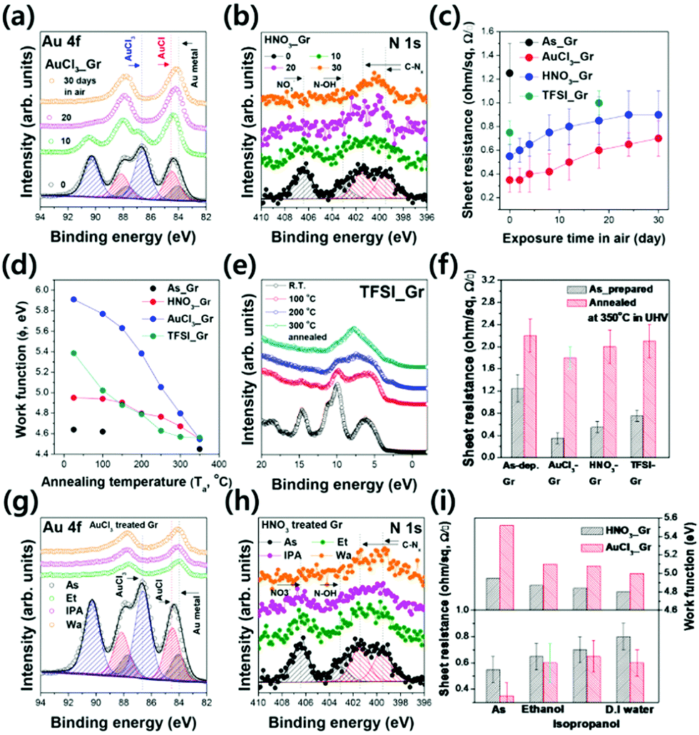 | ||
| Fig. 2 (a) Au 4f core levels of AuCl3_Gr in the XPS spectrum with the aging process, (b) N 1s core levels of HNO3_Gr in the XPS spectrum with the aging process, (c) the changes in sheet resistance of As_Gr, AuCl3_Gr, HNO3_Gr, and TFSI_Gr with the aging process up to 30 days, (d) the changes in work function of As_Gr, AuCl3_Gr, HNO3_Gr, and TFSI_Gr with different annealing temperatures, (e) the changes in the valence band structures of TFSI_Gr with different annealing temperatures, (f) the changes in the sheet resistances of As_Gr, AuCl3_Gr, HNO3_Gr, and TFSI_Gr before/after annealing at 350 °C in ultra-high vacuum (UHV) conditions, (g) Au 4f core levels of AuCl3_Gr in the XPS spectrum with solvent treatment, (h) N 1s core levels of HNO3_Gr in the XPS spectrum with solvent treatment, and (i) the changes in sheet resistance of HNO3_Gr and AuCl3_Gr before/after solvent treatment. | ||
The work function is also a good criterion for examining the Gr doping state. The electron transfer process, which is induced by the electron-donating or withdrawing dopant, involves the Fermi energy level shift of the Gr layer. Thereby, along with the sheet resistance, the work function of the doped Gr layer necessarily varies corresponding to the dopant concentration on the Gr surface.25,26 In order to study the direct correlation between the dopant concentration and work function, we characterized the UPS spectra of the doped Gr layers in the process of thermal annealing under ultrahigh vacuum conditions and the resulting work function data are summarized in Fig. 2(d). The work functions of the Gr layers are calculated using the following eqn (1):
| ΦM = hν − ECutoff + EFermi(electrode) | (1) |
Moreover, the solvent exposure test indicates that the stability of the dopants should be considered as a critical criterion, apart from the doping efficiency. We assumed that the p-type dopant molecules with hygroscopic properties were easily washed away by polar solvents. We prepared three kinds of polar solvents—ethanol, isopropanol, and deionized water—and immersed each of the p-type doped Gr layers in these solvents for 30 seconds. Subsequently, the chemical structures, electronic structures, and sheet resistances were analyzed before and after the solvent exposure, as summarized in Fig. 2(g)–(i). Based on the comparative XPS spectra in Fig. 2(g) and (h), we can determine a significant loss of the electron-withdrawing groups (AuCl or AuCl3 for AuCl3_Gr, NO3− for HNO3_Gr) from the Gr surface. Furthermore, both the work function and sheet resistance of the doped Gr layers exhibited considerable changes, as summarized in Fig. 2(i).
We have clearly elucidated the instability of the Gr doping under various conditions, such as aging under ambient conditions, thermal annealing, and solvent treatment. These results illustrate that the doped Gr layers might have a strong possibility of transition in electronic properties even in the semiconductor/electrode structure of a real device. Thereby, we suggested an analysis method to directly characterize the aging process of the Gr doping states at the semiconductor/electrode interfaces based on in situ UPS/XPS measurements with Ar GCIB sputtering, as well as the enhanced stability of the dopants. Fig. 3(a)–(d) illustrate the UPS spectra obtained before and after C60 layer deposition on the Gr layers (As_Gr, AuCl3_Gr, HNO3_Gr, and TFSI_Gr) and we can determine the energy level alignments at the C60/Gr interfaces. The hole-injection barrier (EHB) at the C60/Gr interface is calculated using eqn (2):
| EHB = EHOMO(organic) − EFermi(electrode) | (2) |
 | ||
| Fig. 3 The UPS spectra obtained before and after C60 (approximately 15 nm) layer deposition on (a) As_Gr, (b) AuCl3_Gr, (c) HNO3_Gr, and (d) TFSI_Gr, and the energy band diagram at the interfaces of (e) C60/As_Gr, (f) C60/AuCl3_Gr, (g) C60/HNO3_Gr, and (h) C60/TFSI_Gr. | ||
Fig. 4 shows the UPS depth profiles of C60/AuCl3_Gr, C60/HNO3_Gr, and C60/TFSI_Gr obtained after an aging process of two weeks under ambient conditions. Except for the oxidized top surface, the C60 layers still preserve their intrinsic electronic structures (Fig. 3), and the HOMO level positions in the UPS spectra enable the determination of the energy level alignments. Through the Ar GCIB sputtering process, we clearly defined the HOMO level and this result provides important information regarding the transition behavior of p-type doped Gr in the C60/Gr structure. After Ar GCIB sputtering for 1 min, the UPS spectra of the C60/Gr structures became similar to the inherent C60 electronic structure such that we could determine the values of the HOMO level. Every C60/p-type doped Gr structure exhibited a higher HOMO level compared to the initial value; however, among them, the C60/TFSI_Gr structure particularly exhibited a significant change in the HOMO level from 1.00 eV to 1.25 eV (C60/AuCl3_Gr: 0.80 eV to 0.86 eV and C60/HNO3_Gr: 1.20 eV to 1.28 eV, after 2 min of Ar GCIB sputtering, shown in Fig. 3 and 4). Besides the UPS analysis, the chemical information in the p-type doped Gr layer in the C60/Gr structure was investigated through the XPS depth profile, and these results illustrated in Fig. 5(a)–(f) elucidate the reason for the energy level distinction after an aging process of two weeks under ambient conditions. Except for a small portion of Au metal on the C60 surface, most dopant molecules (AuCl3, AuCl, and Au metal) of AuCl3_Gr still remained close to their original states despite a continuous attack by reactive molecules including water vapor, carbon dioxide, or oxygen gas. Similarly, the NO3− state of the dopant molecule was also observed in HNO3_Gr in the C60/Gr structure owing to the passivation role of the C60 layer, as shown in Fig. 5(d). On the other hand, the chemical structures of the C60/TFSI_Gr structure were completely different from the others mentioned above. Considering the atomic components of TFSI molecules (C, N, O, F, and S), the XPS results of Fig. 5(e) and (f) indicate that a large percentage of the TFSI molecules on TFSI_Gr transferred from the Gr layer to the C60 surface. More carbon–fluorine bonding was observed on the C60 surface rather than the TFSI_Gr. In other words, a larger number of TFSI molecules were bound with the C60 surface than the Gr layer after an aging process of two weeks under ambient conditions. We believe that this unique phenomenon stems from the TFSI molecules with fluid characteristics.30 The hydrophobic TFSI molecules are inclined to move to the surface as far as possible to reduce the surface energy. Therefore, the resulting decrease of doping effects on the TFSI_Gr led to a huge increase of the EHB from 1.00 eV to 1.25 eV at the C60/TFSI_Gr interface. In addition, we carried out an atomic force microscopy (AFM) measurement in order to investigate the morphology of the Gr layers before and after Gr doping or the C60 deposition process (Fig. 6). While the morphology of TFSI_Gr remains almost the same as As_Gr, the AuCl3 and HNO3 treatments led to a huge change in the surface morphologies of the Gr layers owing to dopant aggregation or wrinkle/ripple formation, as shown in Fig. 6(a) and (b). Nevertheless, all of them remain smooth with their roughness under 2 nm (As_Gr: 1.75 nm, AuCl3_Gr: 1.99 nm, HNO3_Gr: 1.96 nm, and TFSI_Gr: 1.60 nm, calculated based on the corresponding AFM images). Regardless of the doping method, the C60 molecules form a uniform layer with a granular grain structure on the Gr surface (Fig. 6(a)). However, the morphology of the C60 layer grown on TFSI_Gr involves different features. Firstly, as shown in the comparative line profiles of Fig. 6(c), the C60 layer on TFSI_Gr exhibits a relatively higher surface roughness than the others. Moreover, there are several valley- or well-shaped pores, unlike the layers on As_Gr, AuCl3_Gr, and HNO3_Gr, probably due to the movement of TFSI molecules as discussed in the UPS/XPS depth profiles (Fig. 4 and 5).
 | ||
| Fig. 4 The UPS depth profiles of (a) C60/AuCl3_Gr, (b) C60/HNO3_Gr, and (c) C60/TFSI_Gr obtained after an aging process of two weeks under ambient conditions. Each of the UPS spectra were obtained by an additional 1 minute Ar GCIB sputtering process from the bottom. The inset graphs highlight the HOMO level positions of C60 near the Fermi energy. | ||
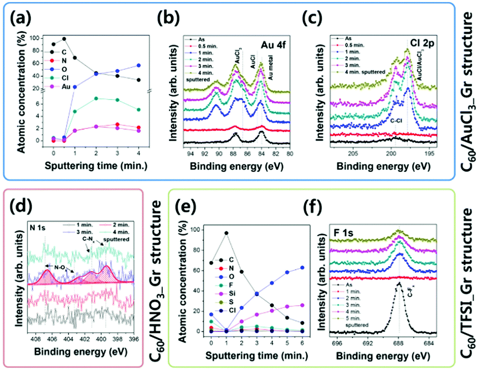 | ||
| Fig. 5 The XPS depth profiles of (a) the atomic concentration of C60/AuCl3_Gr, (b) Au 4f core levels of C60/AuCl3_Gr, (c) Cl 2p core levels of C60/AuCl3_Gr, (d) N 1s core levels of C60/HNO3_Gr, (e) the atomic concentration of C60/TFSI_Gr, and (f) F 1s core levels of C60/TFSI_Gr. | ||
 | ||
| Fig. 6 (a) AFM images of the As_Gr, AuCl3_Gr, HNO3_Gr, and TFSI_Gr layers before and after C60 layer deposition, (b) line profiles of the As_Gr, AuCl3_Gr, HNO3_Gr, and TFSI_Gr layers before C60 layer deposition, and (c) line profiles of the As_Gr, AuCl3_Gr, HNO3_Gr, and TFSI_Gr layers after C60 layer deposition. | ||
We continued the investigation of the electronic and chemical structure changes as a function of aging time of the C60/Gr structures under ambient conditions. Fig. S1(a)–(d) (ESI†) show the chemical states of the C60/Gr structures after one month. In comparison with the XPS spectra in Fig. 4, we could determine the transition behaviors of the doping states in the C60/Gr structures. The amount of dopant molecules on Gr slightly decreases for the same period of time after the initial two-week aging process. The presence of dopant molecules maintains the doping effects on the properties of the doped Gr layer. However, even if it is a subtle change, the doping state transitions of the Gr layer are reflected in the energy level alignments at the C60/Gr interface. The UPS depth profiles of Fig. S2(a)–(d) (ESI†) show the energy level alignments of the C60/As_Gr and C60/p-type doped Gr structures after one month. By comparing the hole injection barriers after an aging process of two weeks and one month, it can be observed that all the EHBs of the C60/p-type doped Gr structures slightly increase corresponding to the dopant chemical states on the Gr layers. (C60/AuCl3_Gr: 0.86 eV to 0.90 eV, C60/HNO3_Gr: 1.28 eV to 1.33 eV, and C60/TFSI_Gr: 1.20 eV to 1.23 eV).
In addition, we continued monitoring the aging process of the C60/Gr structures over a longer period of time. Fig. S3 and S4 (ESI†) show the XPS depth profiles of the C60/p-type doped Gr structures, which were measured after an aging process of two months and three months, respectively. From the XPS depth profiles of C60/HNO3_Gr and C60/TFSI_Gr, we can clearly illustrate the variations of the dopant chemical states. According to aging time, the TFSI concentration on the Gr layer in the C60/TFSI_Gr structure undergoes little change, even though it gradually decreases on the C60 surface. The XPS depth profile of C60/HNO3_Gr does not provide clear information regarding the doping state transition except for the NO3− existence owing to low signal to noise. On the other hand, the Au 4f and Cl 2p XPS core levels of the C60/AuCl3_Gr structure provide significant information on the doping state transition during the aging process under observation, and the (AuCl3 + AuCl)/Au metal ratio is a good criterion for the same. After three months of aging, the chemical states of gold chloride (AuCl + AuCl3) on AuCl3_Gr decreased, whereas the Au metal state underwent little change. Consequently, this transition behavior of the C60/AuCl3_Gr structure is completely analogous with that of a single AuCl3_Gr; however, the only major difference is the time spent for gold chloride reduction owing to the partial passivation effect of the C60 layer (approximately 15 nm) on AuCl3_Gr.
Along with the XPS depth profile analysis, we measured the UPS depth profiles of the C60/Gr structures after three months of aging, as shown in Fig. 7(a) and (b). In spite of the growth of the surface oxide region, all the C60/Gr structures exhibited clear electronic structures at the interface regions; hence, we could determine the energy level alignments including the secondary cut-off and HOMO level positions. The secondary cut-off and HOMO level positions correspond to the vacuum level shifts and hole injection barriers, respectively. The resulting energy level alignments are summarized in Fig. 7(c) and (d). While the energy level alignments reveal little difference between the C60/HNO3_Gr and C60/As_Gr structures, the C60/AuCl3_Gr and C60/TFSI_Gr structures still preserved significantly lower hole injection barriers than the C60/As_Gr structure. Since this relative distinction stems from the doping states of the p-type doped Gr layers, we could determine that both AuCl3_Gr and TFSI_Gr still continue the doping effect even after three months of aging under ambient conditions.
 | ||
| Fig. 7 The comparative (a) secondary cut-off and (b) Fermi level region in the UPS spectra of three month-aged C60/As_Gr, C60/AuCl3_Gr, C60/HNO3_Gr, and C60/TFSI_Gr obtained by the Ar GCIB sputtering process, and the energy level alignments with (c) the secondary cut-off point and (d) the HOMO level position with respect to sputtering time for C60/As_Gr, C60/AuCl3_Gr, C60/HNO3_Gr, and C60/TFSI_Gr. | ||
In addition, the doping states of the Gr layers in the C60/Gr structures were directly investigated by using Raman spectroscopy measurements, after three months of aging under ambient conditions. In comparison with the G-band peak position of As_Gr, the G-band shifts to a relatively higher wavenumber, corresponding to the degree of the p-type doping state in the Gr layer.13,14,23,24 In the Raman spectrum obtained from the C60/Gr structure, the signals from the Gr layer were almost screened by those of the C60 layer. Therefore, we could not peel off the C60 layer from the Gr layer before Raman analysis. The Ar GCIB sputtering process was carried out until the chemical states of the As_Gr or p-type doped Gr layer appeared in the XPS spectra. As shown in Fig. 8(a) and (b), the torn sections induced by the Ar GCIB sputtering led to the growth of a D-band peak at approximately 1350 cm−1. Nevertheless, we could determine the position of the G-band peak (between 1590 cm−1 and 1600 cm−1) obtained from the Raman spectra of the As_Gr and p-type doped Gr layers. We obtained the Raman spectra from three different points and used the resulting average position of the G-band peak as the basis of comparison for each Gr layer in the C60/Gr structure. As shown in Fig. 8(c) and (d), HNO3_Gr showed little right shift in the G-band position, whereas AuCl3_Gr and TFSI_Gr exhibited shifts in the G-band to larger values. In other words, these Raman results confirm the maintenance of the p-type doping effects in AuCl3_Gr and TFSI_Gr after three months of aging and are consistent with the UPS results of the C60/Gr structures.
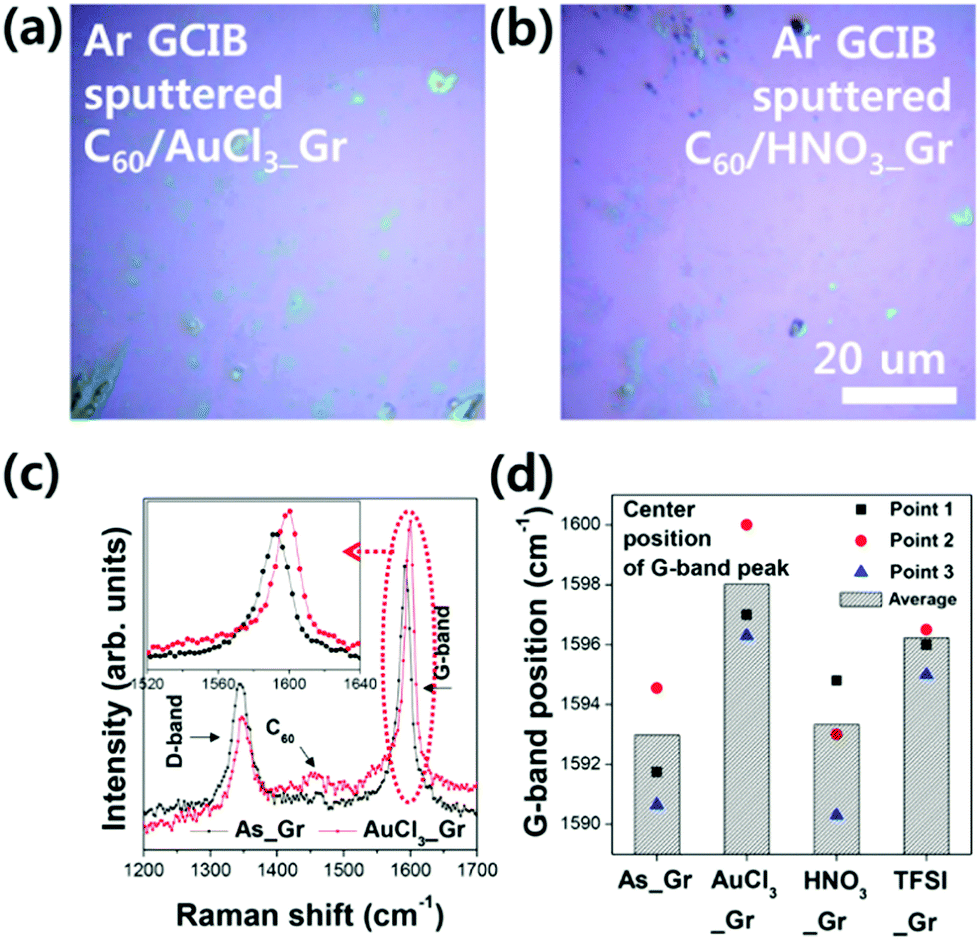 | ||
| Fig. 8 The optical microscopy images of three-month aged (a) C60/AuCl3_Gr and (b) C60/HNO3_Gr after peeling off by the Ar GCIB sputtering process, (c) the Raman spectra of C60/As_Gr and C60/AuCl3_Gr, and (d) the G-band positions in the Raman spectra of C60/As_Gr, C60/AuCl3_Gr, C60/HNO3_Gr, and C60/TFSI_Gr after the Ar GCIB sputtering process. | ||
Conclusions
We suggest a novel methodology that enables us to determine Gr doping states by using the energy level alignments at the OSC/electrode interface. After verifying the instability of Gr doping, we design a method to characterize the doping states of the Gr layers, which are covered with multi-storied organic films. We perform cyclic UPS/XPS measurements and these results provide significant information regarding the variation of the chemical and electronic states in the C60/Gr structures, according to aging time under ambient conditions. In addition, the OSC can also act as a passivating layer to prevent severe degradation of dopants with negligible change in the doping state over one month, while the p-type doped Gr without OSC degrades a lot after one month of aging. Consequently, we determine a strong correlation between the energy level alignment at the C60/Gr interface and the Gr doping state; and therefore, this method enables us to accurately analyze the doping states of the Gr layers, which are located in real OSC/electrode interfaces.Conflicts of interest
There are no conflicts to declare.Acknowledgements
This work was supported by a grant from the Fundamental R&D program for Core Technology of Materials funded by the National Research Foundation (NRF) of Korea (10048035). This work was supported by the Samsung Advanced Institute of Technology.Notes and references
- S.-W. Rhee and D.-J. Yun, J. Mater. Chem., 2008, 18, 5437–5444 RSC.
- D.-J. Yun and S.-W. Rhee, J. Mater. Chem., 2010, 20, 9754–9759 RSC.
- J. Yang, D. Yan and T. S. Jones, Chem. Rev., 2015, 115, 5570–5603 CrossRef CAS PubMed.
- J. Lewis, Mater. Today, 2006, 9, 38–45 CrossRef CAS.
- M. Francardi, L. Balet, A. Gerardino, N. Chauvin, D. Bitauld, L. H. Li, B. Alloing and A. Fiore, Appl. Phys. Lett., 2008, 93, 143102 CrossRef.
- S. Kim, H.-J. Kwon, S. Lee, H. Shim, Y. Chun, W. Choi, J. Kwack, D. Han, M. Song, S. Kim, S. Mohammadi, I. Kee and S. Y. Lee, Adv. Mater., 2011, 23, 3511–3516 CrossRef CAS PubMed.
- K. S. Kim, Y. Zhao, H. Jang, S. Y. Lee, J. M. Kim, K. S. Kim, J.-H. Ahn, P. Kim, J.-Y. Choi and B. H. Hong, Nature, 2009, 457, 706–710 CrossRef CAS PubMed.
- Y. Shi, K. K. Kim, A. Reina, M. Hofmann, L.-J. Li and J. Kong, ACS Nano, 2010, 4, 2689–2694 CrossRef CAS PubMed.
- S. Bae, H. Kim, Y. Lee, X. Xu, J.-S. Park, Y. Zheng, J. Balakrishnan, T. Lei, H. Ri Kim, Y. I. Song, Y.-J. Kim, K. S. Kim, B. Ozyilmaz, J.-H. Ahn, B. H. Hong and S. Iijima, Nat. Nanotechnol., 2010, 5, 574–578 CrossRef CAS PubMed.
- S. Wang, P. K. Ang, Z. Wang, A. L. L. Tang, J. T. L. Thong and K. P. Loh, Nano Lett., 2010, 10, 92–98 CrossRef CAS PubMed.
- S. Ye and W.-C. Oh, J. Korean Ceram. Soc., 2017, 54, 28–32 CrossRef CAS.
- T. Kobayashi, M. Bando, N. Kimura, K. Shimizu, K. Kadono, N. Umezu, K. Miyahara, S. Hayazaki, S. Nagai, Y. Mizuguchi, Y. Murakami and D. Hobara, Appl. Phys. Lett., 2013, 102, 023112 CrossRef.
- A. Kasry, M. A. Kuroda, G. J. Martyna, G. S. Tulevski and A. A. Bol, ACS Nano, 2010, 4, 3839–3844 CrossRef CAS PubMed.
- S. M. Kim, Y. W. Jo, K. K. Kim, D. L. Duong, H.-J. Shin, J. H. Han, J.-Y. Choi, J. Kong and Y. H. Lee, ACS Nano, 2010, 4, 6998–7004 CrossRef CAS PubMed.
- Y. Ji, S. Lee, B. Cho, S. Song and T. Lee, ACS Nano, 2011, 5, 5995–6000 CrossRef CAS PubMed.
- X. Wang, L. Zhi and K. Müllen, Nano Lett., 2008, 8, 323–327 CrossRef CAS PubMed.
- C. W. Jang, J. M. Kim, J. H. Kim, D. H. Shin, S. Kim and S.-H. Choi, J. Alloys Compd., 2015, 621, 1–6 CrossRef CAS.
- D.-J. Yun, J. Chung, Y. Kim, S.-H. Park, S.-H. Kim and S. Heo, J. Appl. Phys., 2014, 116, 153702 CrossRef.
- D.-J. Yun, J. Kim, J. Chung, S. Park, W. Baek, Y. Kim, S. Kim, Y.-N. Kwon, J. Chung, Y. Kyoung, K.-H. Kim and S. Heo, J. Power Sources, 2014, 268, 25–36 CrossRef CAS.
- R. Younesi, M. Hahlin, M. Treskow, J. Scheers, P. Johansson and K. Edström, J. Phys. Chem. C, 2012, 116, 18597–18604 CAS.
- J. Maibach, C. Xu, S. K. Eriksson, J. Åhlund, T. Gustafsson, H. Siegbahn, H. Rensmo, K. Edström and M. Hahlin, Rev. Sci. Instrum., 2015, 86, 044101 CrossRef PubMed.
- J. W. Suk, A. Kitt, C. W. Magnuson, Y. Hao, S. Ahmed, J. An, A. K. Swan, B. B. Goldberg and R. S. Ruoff, ACS Nano, 2011, 5, 6916–6924 CrossRef CAS PubMed.
- K. C. Kwon, K. S. Choi and S. Y. Kim, Adv. Funct. Mater., 2012, 22, 4724–4731 CrossRef CAS.
- K. C. Kwon, B. J. Kim, J.-L. Lee and S. Y. Kim, J. Mater. Chem. C, 2013, 1, 2463–2469 RSC.
- D. H. Shin, J. M. Kim, C. W. Jang, J. H. Kim, S. Kim and S.-H. Choi, J. Appl. Phys., 2013, 113, 064305 CrossRef.
- S.-K. Lee, K. Rana and J.-H. Ahn, J. Phys. Lett., 2013, 4, 831–841 CAS.
- W.-H. Lin, T.-H. Chen, J.-K. Chang, J.-I. Taur, Y.-Y. Lo, W.-L. Lee, C.-S. Chang, W.-B. Su and C.-I. Wu, ACS Nano, 2014, 8, 1784–1791 CrossRef CAS PubMed.
- D.-J. Yun, J. Chung, S. H. Kim, Y. Kim, S. Park, M. Seol and S. Heo, Nanotechnology, 2015, 26, 465704 CrossRef PubMed.
- D.-J. Yun, T. Shin, S. Park, Y. Shin, Y. Kyung, J. Chung and Y. Kim, RSC Adv., 2015, 5, 77814–77822 RSC.
- A. Ghoufi, A. Szymczyk and P. Malfreyt, Sci. Rep., 2016, 6, 28518 CrossRef PubMed.
Footnote |
| † Electronic supplementary information (ESI) available: Fig. S1–S4. See DOI: 10.1039/c7cp06450k |
| This journal is © the Owner Societies 2018 |