
The role of PbI2 in CH3NH3PbI3 perovskite stability, solar cell parameters and device degradation†
Tanaji P.
Gujar
a,
Thomas
Unger
b,
Andreas
Schönleber
 c,
Martina
Fried
a,
Fabian
Panzer
b,
Sander
van Smaalen
c,
Anna
Köhler
b and
Mukundan
Thelakkat
*a
c,
Martina
Fried
a,
Fabian
Panzer
b,
Sander
van Smaalen
c,
Anna
Köhler
b and
Mukundan
Thelakkat
*a
aApplied Functional Polymers, Macromolecular Chemistry I, University of Bayreuth, 95447 Bayreuth, Germany. E-mail: Mukundan.Thelakkat@uni-bayreuth.de
bExperimental Physics II, University of Bayreuth, 95447 Bayreuth, Germany
cLaboratory of Crystallography, University of Bayreuth, 95447 Bayreuth, Germany
First published on 21st November 2017
Abstract
We report a systematic investigation on the role of excess PbI2 content in CH3NH3PbI3 perovskite film properties, solar cell parameters and device storage stability. We used the CH3NH3I vapor assisted method for the preparation of PbI2-free CH3NH3PbI3 films under a N2 atmosphere. These pristine CH3NH3PbI3 films were annealed at 165 °C for different time intervals in a N2 atmosphere to generate additional PbI2 in these films. From XRD measurements, the excess of PbI2 was quantified. Detailed characterization using scanning electron microscopy, X-ray diffraction, UV-Visible and photoluminescence for continuous aging of CH3NH3PbI3 films under ambient condition (50% humidity) is carried out for understanding the influence of different PbI2 contents on degradation of the CH3NH3PbI3 films. We find that the rate of degradation of CH3NH3PbI3 is accelerated due to the amount of PbI2 present in the film. A comparison of solar cell parameters of devices prepared using CH3NH3PbI3 samples having different PbI2 contents reveals a strong influence on the current density–voltage hysteresis as well as storage stability. We demonstrate that CH3NH3PbI3 devices do not require any residual PbI2 for a high performance. Moreover, a small amount of excess PbI2, which improves the initial performance of the devices slightly, has undesirable effects on the CH3NH3PbI3 film stability as well as on device hysteresis and stability.
Introduction
Organometal halide perovskite solar cells have achieved great progress in the last few years. The power conversion efficiency (PCE) of CH3NH3PbI3 perovskite based thin film photovoltaic devices has already reached a high value of 22% in just a few years.1 This rapid progress was achieved by optimizing both the material and device architecture and understanding the underlying photoinduced charge separation mechanisms of these devices.2–11 Major efforts have been made to achieve high efficiency using various approaches comprising passivation of defects12 and tuning and controlling numerous parameters in perovskite layers such as the surface morphology,13 grain size,14 different halogen ratio15,16 and different cation compositions (mixture of CH3NH3/HC(NH2)2).17 Additionally, both the charge extraction layers, the electron transport layer (ETL)7 and the hole transport layer (HTL),18 have also been studied and optimized. Several recent papers reveal that one of the preferred techniques to improve the PCE of CH3NH3PbI3 is using excess PbI2, which is not converted to CH3NH3PbI3. For example, Chen et al. demonstrated the role of PbI2 in CH3NH3PbI3 for the improvement of device performance by annealing after preparing pristine CH3NH3PbI3 using the CH3NH3I (MAI)-vapor assisted method.12 Kim et al. demonstrated that 5.7 wt% PbI2 in the (CH(NH2)2PbI3)0.85(CH3NH3PbBr3)0.15 perovskite prepared using the solvent engineering method improved the PCE as well as reduced the hysteresis.17 Roldan-Carmona et al. observed that 10 wt% additional PbI2 in CH3NH3PbI3 using the solvent engineering method is beneficial for the improvement of PCE of devices.19 It was also reported that 2 wt% residual PbI2 in CH3NH3PbI3 is beneficial to improve the device efficiency.20 Moreover, the benefits of PbI2 in CH3NH3PbI3 towards an improved performance can be inferred from the fact that most of the high PCE perovskite solar cells prepared using a variety of methods exhibited unintentionally a small amount of excess PbI2.21,22 Jacobsson et al.23 also confirmed that the hysteresis index in (CH(NH2)2PbI3)0.85(CH3NH3PbBr3)0.15 devices is higher for samples having a residual PbI2 content compared to the PbI2-deficient samples. Based on this, it was suggested that excess PbI2 in CH3NH3PbI3 can help to passivate defects at surfaces and grain boundaries12 and a small amount of residual PbI2 in the perovskite supports reduction of charge recombination and improves open circuit voltage (Voc) and the fill factor (FF).17 It has also been suggested that the small amount of excess PbI2 in the perovskite influences the morphology and increases the size as well as the uniformity of perovskite crystals using the solvent engineering method.19,24On the other hand, it is noteworthy that for PbI2-free CH3NH3PbI3 solar cells using a modified MAI-vapor assisted method for CH3NH3PbI3 crystallization, we clearly demonstrated a reproducible performance with ∼15% PCE.25 Li et al. have a similar observation that a high PCE of 14.2% can be achieved for PbI2-free CH3NH3PbI3 prepared using a low pressure MAI-vapor assisted method.26 While considering the excess PbI2 for high PCE perovskite solar cells, one should not overlook the fact that PbI2 in perovskites exhibits intrinsic instability under illumination.27 Liu et al. demonstrated that residual PbI2 accelerates the degradation of CH3NH3PbI3 films upon exposure to illumination.27 Encapsulated devices have the same stability performance like excess PbI2-free CH3NH3PbI3 devices. Thus, the influence of PbI2 in perovskite films on solar cells is moderately known but their influence on degradation or stability is ambiguous. It is therefore of great interest to study systematically the effect of PbI2 in CH3NH3PbI3 not only on the PCE of solar cells, but also on their photophysics and stability, since both long term stability and a high PCE are essential for practical applications. For a comprehensive investigation of the effect of PbI2, it is necessary to consider separately the effects caused by PbI2 in CH3NH3PbI3 on absorption/emission, morphology, decomposition of the perovskite layer, device parameters and the overall device stability. Thus the open questions that we address are (1) what is the influence of residual PbI2 on the stability of the perovskite films and morphology? (2) Can we observe any quantifiable trend in the PL properties and PbI2 content? (3) How far is the beneficial effect of PbI2 counteracting the performance and stability of the devices? and (4) Is it possible to separate the different positive and negative effects to make conclusion on the net effect of residual PbI2?
We used the MAI-vapor assisted method for the preparation of CH3NH3PbI3 films under a N2 atmosphere.25 With this method we guarantee uniform film formation with similar grain sizes and high reproducibility and stability of the CH3NH3PbI3 films.25,28 There are three ways to introduce PbI2 in such films: (a) by prolonged thermal annealing of a PbI2-free film12 or (b) by purposefully adding non-stoichiometric amounts of precursors to obtain residual non-converted PbI2 in the final perovskite17,19 or (c) partial conversion of PbI2 to CH3NH3PbI3.21,22 We adopted the first method to obtain samples with different amounts of PbI2 by annealing the samples at 165 °C for different time intervals in a N2 atmosphere. Characterization using scanning electron microscopy (SEM), X-ray diffraction (XRD), UV-Visible and photoluminescence (PL) with aging of CH3NH3PbI3 films under ambient conditions (50% humidity) is carried out for understanding the influence of residual PbI2 on the stability of CH3NH3PbI3 itself. A comparison of solar cell parameters for the different CH3NH3PbI3 samples with varying PbI2 contents is also performed. We demonstrate that a solar cell device with a very small amount of excess PbI2 can exhibit a slightly higher PCE, but this small amount of excess PbI2 has undesirable effects on the CH3NH3PbI3 film stability, current density–voltage (J/V) hysteresis and device stability. The presence of a small amount of excess PbI2 results in the faster degradation of the CH3NH3PbI3 layer in a humid air atmosphere and the degradation rate increases with the amount of additional PbI2 in CH3NH3PbI3 films. Thus, this work gives insights into the overall consequences of residual PbI2 on different aspects of CH3NH3PbI3 solar cells. This work confirms the initial positive influence of excess PbI2 on CH3NH3PbI3 solar cell devices but simultaneously also proves that it accelerates film degradation and therefore limits device lifetime.
Experimental section
Materials
All starting materials were purchased from Sigma-Aldrich and used as received. Spiro-OMeTAD was purchased from Merck Chemicals.MAI synthesis
MAI was synthesized by reacting 24 mL of methylamine (33 wt% in absolute ethanol) and 10 mL of hydroiodic acid (57 wt% in water) in a round-bottom flask at room temperature (RT) for 2 h under Ar with stirring. The raw precipitate was recovered by removing the solvent in a rotary evaporator at 40 °C. The raw product was washed with ethyl ether, dried in a vacuum at RT and redissolved in absolute ethanol. The pure MAI recrystallized upon cooling is filtered and dried at RT in a vacuum oven for 24 h. The purity of MAI is very crucial for the synthesis of a pure perovskite.Device fabrication
Fluorine doped tin oxide (FTO)-coated glass sheets (17 Ω □−1) were etched with zinc powder and HCl (2 M) to obtain the required electrode pattern. The substrates were then cleaned with a detergent followed by sonication in deionized water, acetone and ethanol for 10 min each, and dried with clean dry air. A 50 nm compact-TiO2 (c-TiO2) blocking layer was deposited by spray pyrolysis of titanium(IV) bis(acetoacetonato)–di(isopropanoxylate) diluted in ethanol at 450 °C on FTO-coated glass substrates and annealed at 450 °C for 1 h. After cooling, the substrates were transferred in a glovebox under a N2 atmosphere. For CH3NH3PbI3 formation, we adapted a published procedure12,25,28 and optimized it as follows. PbI2 (1 M) was dissolved in N,N-dimethyl formamide overnight under stirring conditions at 100 °C and 80 μL solution was spin coated on the FTO/c-TiO2 substrates at 2000 rpm for 50 s, and dried at 100 °C for 5 min. 100 mg MAI powder was spread out around the PbI2 coated substrates with a Petri dish covering on the top and heated at 165 °C for 13 h for full conversion. Subsequently, the as-prepared samples were annealed at 165 °C for different time intervals to generate residual PbI2. The HTL deposition solution comprised of 2,2′,7,7′-tetrakis-(N,N-di-p-methoxyphenylamine) 9,9′-spirobifluorene (spiro-OMeTAD) in chlorobenzene (102.85 mg mL−1), 40 mL of 4-tert-butylpyridine and 37 mL (520 mg mL−1) solution of bis(trifluoromethane) sulfonimide lithium salt (LiTFSI) in acetonitrile. This solution was spin coated at 2000 rpm for 30 s under N2 conditions and stored in dry air overnight. No oxidants were used. This was followed by thermal deposition of gold to form the back contact. The active areas of the devices fabricated in this work are 0.09 and 0.16 cm2.Characterization
The structural and phase characterization of the CH3NH3PbI3 layer deposited on the FTO/c-TiO2 substrate was carried out in the reflection mode XRD using a Panalytical X'pert pro diffractometer with Cu Kα1 radiation (λ = 0.15405 nm), operated at 40 kV and 40 mA. The diffractograms were recorded in the 2θ range of 10 to 45° with a 2θ step size of 0.008°. UV-Vis absorption spectra were collected using a V-630 UV-Vis Jasco Spectrophotometer coupled with an integrating sphere. The surface morphology and cross-section were characterized by field emission SEM using a Zeiss 1530 instrument with an accelerating voltage of 3.0 kV. PL spectra and PL quantum yield were recorded of CH3NH3PbI3 deposited on quartz substrates with an integrating sphere coupled via optical fiber to a Oriel spectrograph MS125 and a Andor Idus CCD camera. The excitation source is a 485 nm laser diode LDH-D-C-485, PicoQuant GmbH. The used intensity was about 450 mW cm−2. Each sample is measured after 2 min of laser exposure in order to account for the “soaking effect”.29,30 The exposure time is kept constant for all measurements. The influence of the soaking effect was investigated for each sample at day 1 (see Fig. S1 in the ESI†). The J/V plots of solar cell devices were obtained using an Oriel solar simulator under AM 1.5, 1000 W m−2 conditions. The J/V data under these conditions were obtained using a Keithley model 2400 source meter. All J/V measurements were performed in a N2 atmosphere. Both forward (from −1 V to +2 V) and backward (from +2 V to −1 V) sweeps were recorded to understand the hysteresis. All the devices were measured at a sweep rate of 100 mV s−1. Each device was equilibrated by multiscans in reverse mode under illumination till the short circuit current density (Jsc) was stabilized. Each device type was fabricated in two batches (4 devices each) and analyzed to understand the scattering of device parameters.Results and discussion
XRD analysis of the residual PbI2 content and the influence on the morphology
For generation of PbI2 in CH3NH3PbI3 films, we used thermal annealing of pure CH3NH3PbI3 films at 165 °C for different time intervals (0, 15, 30, 45 and 60 min) and the five samples obtained are mentioned in the following as A, B, C, D and E, respectively. To monitor the generation of PbI2 by annealing and to verify the comparative amount of PbI2 in the processed CH3NH3PbI3 material, XRD experiments have been performed for all samples including pure PbI2 (Fig. 1a). The X-ray patterns confirm the presence of the tetragonal perovskite phase of CH3NH3PbI3 in all of the prepared films. In sample A, XRD pattern shows that the films composed of a single pristine perovskite phase with strong diffraction peaks (110), (220) and (114), characteristic of CH3NH3PbI3 in the tetragonal phase. No peaks of PbI2 could be detected. The PbI2 phase in the pure perovskite can be identified by the characteristic PbI2 peak located at 2θ ∼ 12.7°. Accordingly, for sample B, a small PbI2 peak becomes apparent at 2θ of 12.7°. With increasing annealing time, the characteristic PbI2 peak increases in intensity from sample B to E on the concomitant expense of the intensity of the (110) peak of the perovskite at about 15°. Fig. 1b shows that the amount of PbI2 present in the pervoskite films and PbI2 wt% rapidly increase with an increase in the annealing time, confirming this interconversion during thermal annealing. An increase of PbI2 amounts in the films as obtained from XRD is confirmed by PbI2 wt% calculated from optical measurements and both values agree very well. As per XRD measurements, the samples A to E have 0, 21, 34, 46 and 48 wt% PbI2 respectively. Detailed calculations of PbI2 wt% in CH3NH3PbI3 films from XRD and optical spectroscopy (Fig. S2 and S3) are explained in the ESI.†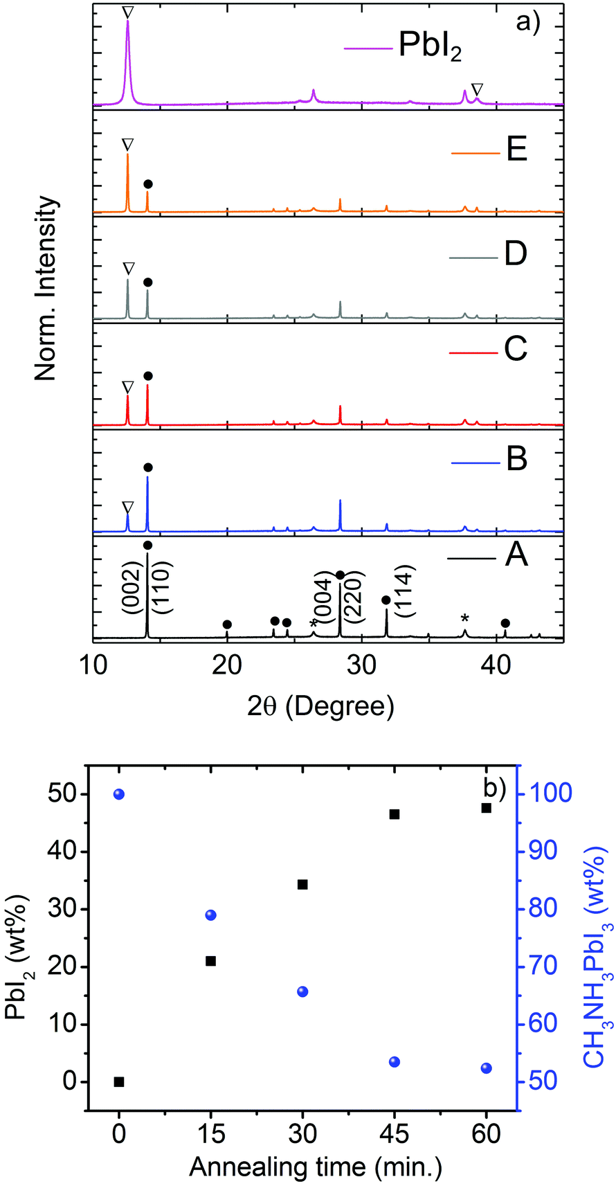 | ||
| Fig. 1 (a) XRD patterns of CH3NH3PbI3 samples on compact TiO2 annealed at 165 °C for (A) 0 min, (B) 15 min, (C) 30 min, (D) 45 min and (E) 60 min; (b) PbI2 wt% and CH3NH3PbI3 wt% with annealing time. XRD peaks are labeled for CH3NH3PbI3 (black dot), PbI2 (open triangle) and substrate (black star). | ||
SEM images obtained from the surface analysis of the CH3NH3PbI3 films A, B, C and E are shown in Fig. 2, which illustrate the changes in the grain-size upon annealing. Since there is no detectable difference for samples D and E, the image of sample D is given in Fig. S4 (ESI†). From the surface view of sample A, it is clear that the CH3NH3PbI3 films are composed of micrometer-sized grains that exhibit a densely packed morphology and are free from pinholes/pores. The average grain size is 1000 nm. From sample B to E, compactness of the samples decreases as well as edges of grains vanish from sample B to E. Especially in sample E, one can observe loss of matter at the grain boundaries, which suggest that with a prolonged annealing time, the PbI2 content increases by evaporation of MAI at grain boundaries and probably at the surface of the film as well. The cross-sectional SEM of samples A to E (Fig. S4, ESI†) does not show any clear separation/gap between the grains in the bulk of the film. According to Chen et al., CH3NH3PbI3 decomposed upon prolonged annealing at 150 °C and conversion from CH3NH3PbI3 to PbI2 occurred where CH3NH3I species escaped from the perovskite film to form the PbI2 phase mostly at grain boundaries and at the relevant interfaces.12 Xie et al. also confirmed the existence of PbI2 on the surface formed by decomposition of CH3NH3PbI3 by annealing at 150 °C.31 However, in our case it seems most decomposition happens at the surface, but it is difficult to exactly depict the location regarding the presence/distribution of PbI2 in these films just from SEM analysis.
 | ||
| Fig. 2 SEM images of CH3NH3PbI3 samples A, B, C and E at magnification 10 KX. The SEM image of sample D is very similar to that of sample E and is shown in Fig. S4 (ESI†). | ||
Influence of PbI2 on the optical properties
Fig. 3a shows the absorption spectra of samples A to E. The initial thicknesses of all samples were similar and lie in the range of 300 to 325 nm. The position of band-edge absorption of all samples is almost the same but the absolute absorbance at 700 nm for samples A to E indicates that the optical density decreases. It is obvious that, from samples A to E, the CH3NH3PbI3 amount in the film decreases with an increase in the PbI2 content. In the absorption graph for samples B to E, a kink (shoulder) is observed at 500 nm and its intensity increased from sample B to E. Upon comparison to the PbI2 absorption (Fig. 3a), this is indicative of an increased amount of the PbI2 content in the CH3NH3PbI3 films. To obtain the band gap (Eg), these data were further analyzed using the classical Tauc relation, for direct optical gap semiconductors: α = A(hν − Eg)n/hν, where α is the absorption coefficient, A is the proportionality constant, n = 0.5 for direct band gap materials and hν = photon energy. The plots of (αhν)2versus hν of the CH3NH3PbI3 films are shown in Fig. 3b. This graph gives Eg, when a straight portion of (αhν)2 against the hν plot is extrapolated to the point α = 0. For all samples it is around 1.6 eV, thus independent of the excess PbI2 content and consistent with recent literature reports.32,33 | ||
| Fig. 3 (a) UV-Visible absorption spectra of samples A to E and PbI2 film; (b) plots of (αhν)2 against hν of all CH3NH3PbI3 samples; (c) steady-state photoluminescence (PL) for all samples. | ||
Fig. 3c shows the steady-state PL spectra of the different samples on quartz substrates without any protection layers on top and measured in humid air (50% humidity). While sample A does not show any PL, the PL intensity increases from sample B to E and the peak position stays constant around 780 nm (1.59 eV).
Influence of PbI2 on degradation of perovskite films
A second series of XRD measurements were performed to explore the film stability and the degree of degradation of the pristine CH3NH3PbI3 and PbI2 containing CH3NH3PbI3 films over time in humid air. Fig. 4 shows the typical XRD patterns of CH3NH3PbI3 samples A (no PbI2), B (least PbI2) and E (highest PbI2) over time in a controlled 50% humid atmosphere. For sample A, strong characteristic peaks of the CH3NH3PbI3 tetragonal structure are observed on the first day, after 15 days and after 30 days of storage. There is no observable change in the XRD pattern between the pristine CH3NH3PbI3 film and the CH3NH3PbI3 film after 15 days of storage at 50% humidity as well as after 30 days. For sample B, the diffraction characteristic peaks of the CH3NH3PbI3 structure (at 2θ = 14.2°) along with PbI2 characteristic peak at a 2θ value of 12.7° are observed on day 1. After storage of 15 days in 50% humidity, the intensity of the (110) peak at a 2θ value of 14.2° is slightly decreased and the PbI2 peak intensity is increased. After 30 days of storage, the peak intensity of PbI2 is significantly increased with a radical decrease of the CH3NH3PbI3 (110) peak intensity. For sample E (the highest PbI2 content with respect to CH3NH3PbI3), the CH3NH3PbI3 diffraction characteristic (110) peak intensity is lower than the PbI2 characteristic peak on the first day. The (110) peak intensity is drastically decreased with an increase in the PbI2 peak after 15 days of storage of sample E. After 30 days, the PbI2 peak intensity is increased and CH3NH3PbI3 peaks appear with a very low intensity. | ||
| Fig. 4 XRD patterns of pure and PbI2 containing CH3NH3PbI3 samples obtained upon air exposure for different periods (at 50% humidity), (a) samples A, (b) sample B and (c) sample E. The peaks assigned: black dot for CH3NH3PbI3 and open triangle for PbI2. | ||
The degradation mechanism of CH3NH3PbI3 in the presence of water, high and low relative humidity has been already suggested by different authors in reactions (1)–(3) below.34–40
According to the literature, pure CH3NH3PbI3 likely reacts with water from humid air and forms non-soluble PbI2 and aqueous CH3NH3I (reaction (1)).35,36 At higher (>80%) humidity CH3NH3PbI3 reacts with water and forms (CH3NH3)4PbI6·2H2O (reaction (2)).34,37,38 In the presence of lower (<50%) humidity CH3NH3PbI3 decomposes into CH3NH2, HI, PbI2 with an irreversible reaction as given in eqn (3).39,40
 | (1) |
 | (2) |
 | (3) |
 | (4) |
In our experiment, the CH3NH3PbI3 films (sample A) are highly air-stable robust materials that do not show any PbI2 peaks due to degradation for up to 30 days, similar to the observations of Christians et al.34 However, when PbI2 is present in CH3NH3PbI3, most probably a non-reversible reaction (4) takes place producing volatile (CH3NH2). Thus, as observed in our experiments, this degradation process is faster for the excess PbI2 content in CH3NH3PbI3 compared to the PbI2-free CH3NH3PbI3 samples. Based on these observations, it is clear that PbI2 acts as a catalyst for the degradation of CH3NH3PbI3 as we suggest in the reaction (4).
To understand the stability of the CH3NH3PbI3 films stored under ambient condition with 50% humidity, we tracked the normalized absorbance of the film at 700 nm for samples A, B, C, D and E for a month (Fig. 5a). The complete spectral change for each sample is given in Fig. S5 (ESI†). Absorbance measurements made on CH3NH3PbI3 films with different amounts of PbI2 content generated by annealing of the CH3NH3PbI3 sample show the typical spectral features of CH3NH3PbI3 with PbI2 on first day. Thus the rate of decrease of the absorbance intensity at 700 nm increases from sample B to E and it is the highest for sample E. To summarize the changes in absorption with storage time, we have additionally plotted the change in optical absorbance with storage time in 50% humidity for the two extreme cases; for sample A without any residual PbI2 and E having an appreciable amount of PbI2 (Fig. 5b). For sample A, overlap of the optical spectra for the first 15 days is observed and only a negligible change is observed after 30 days. The optical absorption curves in Fig. 5a and Fig. S5a (ESI†) do not show characteristic peaks from PbI2, however the absorption curves show a slight decline after 30 days, even though no degradation could be confirmed in XRD studies. Thus we believe that the observed negligible decline of absorbance after 30 days could be due to the surface interaction of the perovskite with humidity in those samples during optical measurements. Additionally, at the very first degradation stage, where only negligible PbI2 is present, PbI2 may not be detected by our used XRD set up, but it may be sensitive enough for optical measurements. In contrast, for sample E the decrease is much stronger and the shoulder at 500 nm (arising out of PbI2 absorption, see Fig. 3a) gets more pronounced with storage time. Sample A shows the least change in the optical spectra. The increased rate of absorbance loss indicates that PbI2 in the samples B to E accelerates the rate of degradation.
 | ||
| Fig. 5 (a) Normalized absorbance at 700 nm of CH3NH3PbI3 samples A to E stored under 50% RH as a function of time (for 0–30 days); dotted lines are linear fits to guide the eye. (b) Comparative decay of UV-Visible absorption of samples A and E stored under 50% relative humidity for 0, 15 and 30 days. (c) Integrated PL intensity for the different samples over storage time under 50% relative humidity. Dotted lines are 2nd order polynomial fits to serve as guide to the eye (see ESI,† Table S2 for fit parameters). | ||
The PL emission studies on samples without and with PbI2 content give further insight into the role of PbI2 in degradation. All the samples were stored under the same conditions of 50% humidity for about 60 days. We observed that samples A to E show different evolutions in the integrated PL intensity over time (Fig. 5c). The pure CH3NH3PbI3 (sample A) with hardly any initial PL emission (Fig. 3c) continuously increased in the PL intensity with a storage time of up to 58 days.
For sample B, PL emission is observed from the first day onwards and it increased up to 38 days; and afterwards decreased continuously. A similar trend is observed for sample C, yet the PL peak emission is reached already after 20 days. Sample D (not shown here) and E have similar PL emission spectra over time. For both samples, PL emission decreased from the first day onwards. The integrated intensity first increases and reaches its maximum even before 20 days for both D and E samples. The peak position shifts to shorter times with increasing excess PbI2 and the peak intensity reduces. This indicates that whenever samples have some amount of PbI2, it helps to increase PL emission, but also deteriorates the PL efficiency for a long term. The actual mechanisms of PbI2 in PL enhancement are still topics of ongoing discussion. As widely accepted in the literature, the main mechanism is related to trap-filling effects.41 Degradation of the perovskite structure is accompanied by a blue shift of the PL peak position, which is also seen here (see S6 in ESI†).42 Moreover, the evolution of the PL intensity with time correlates with the content of PbI2. This suggests that a small fraction of PbI2 reduces non-radiative recombination, a higher fraction leads to a decrease in the PL intensity. The relative change in PL is a sensitive tool that indicates the degradation of the CH3NH3PbI3 films.
Influence of the PbI2 content on solar cell parameters and hysteresis
To comparatively study the influence of the PbI2 content on the photovoltaic parameters, simple planar devices (glass/FTO/c-TiO2/CH3NH3PbI3/spiro-OMeTAD/Au) without any mesoporous TiO2 layers were prepared using samples A, B, C, D and E under N2 and investigated. The J/V plots of the best devices are illustrated in Fig. 6. All of the data presented here are obtained in the reverse scan from +2.0 to −1.0 V at 100 mV s−1. The solar cell parameters of the best-performing devices and average PCE values (of 8 devices for each type from 2 batches) are listed in Table 1. The scattering of solar cell parameters for devices with samples A to E is given in Table S3 (ESI†). The device based on sample A exhibits a Jsc of 15.18 mA cm−2, a Voc of 0.90 V, and 69% FF with a maximum PCE of 10.80% (average: 9.12% and constant output PCE at VMPP = 9.4%). For B, where even though a small amount of CH3NH3PbI3 has been consumed for the formation of PbI2, the Jsc (17.22 mA cm−2) and Voc (0.94 V) values are improved and consequently a higher PCE of 11.00% (average: 10.17%) is obtained. For devices based on samples C to E (with an increase in the PbI2 content), Jsc decreases from 16.15 to 13.30 mA cm−2, Voc from 0.94 to 0.87 V as well as the FF from 66.88 to 56.37%. The decrease of Jsc from sample B to E is obvious because of a considerable reduction of the CH3NH3PbI3 material in the active layer by decomposition and formation of PbI2 upon annealing. It can be observed from Fig. 6 that CH3NH3PbI3 solar cells fabricated from both samples, A without PbI2 as well as B with PbI2, exhibit excellent performance. The difference in average values for all the parameters is not considerable, even though the sample B exhibits the best performance. This is in agreement with numerous reports, which suggested to add a small amount of PbI2 to improve the solar cell performance. Furthermore, the series and shunt resistances (Rs and Rsh) of the various devices were determined from illuminated J/V curves at Voc and Jsc, respectively, and are listed in Table 1. From sample A to C, the Rs value decreased from 8.33 to 5.78 Ω cm2, and it again increases from sample C to E, with an increase in the PbI2 content. This has an obvious detrimental effect on charge transport as observed in the low Jsc and FF values. Among samples A to D, the device using sample A has the lowest Rsh value, which suggests that sample A has the highest carrier recombination within the device for the given geometry and contacts. | ||
| Fig. 6 (a) J/V characteristics of CH3NH3PbI3 solar cell for samples A to E, (b) influence of scanning directions on J/V characteristics of the CH3NH3PbI3 solar cell for samples A and E. For the forward bias from −1 V to +2 V and for the reverse bias from +2 V to −1 V measured under simulated AM 1.5 100 mW cm−2 sun light at scan rate 100 mV s−1; the hysteresis indices for CH3NH3PbI3 solar cells employing samples A to E with increasing PbI2 content are given in Table 1. The J/V assigned: filled symbol for reverse scan and open symbol for forward scan. | ||
| Samples | J sc (mA cm−2) ±σ | V oc (V) | FF (%) | PCE (%) | R s (Ω cm2) | R sh (Ω cm2) | HI |
|---|---|---|---|---|---|---|---|
| A (0 min) | 16.7 (15.1 ± 0.8) | 0.94 (0.92 ± 0.03) | 68 (65 ± 4) | 10.8 (9.1 ± 1.1) | 8.33 | 831 | 0.22 |
| B (15 min) | 17.2 (16.3 ± 0.8) | 0.94 (0.94 ± 0.02) | 68 (67 ± 2) | 11.0 (10.2 ± 0.5) | 7.41 | 2219 | 0.27 |
| C (30 min) | 16.6 (16.2 ± 0.4) | 0.95 (0.94 ± 0.01) | 67 (64 ± 4) | 10.6 (9.7 ± 0.7) | 5.78 | 1875 | 0.34 |
| D (45 min) | 14.9 (14.8 ± 0.3) | 0.90 (0.90 ± 0.02) | 68 (61 ± 6) | 9.1 (8.2 ± 0.7) | 7.87 | 7013 | 0.40 |
| E (60 min) | 12.81 (13.3 ± 0.8) | 0.92 (0.87 ± 0.04) | 59 (56 ± 6) | 7.0 (6.5 ± 0.5) | 8.33 | 2146 | 0.43 |
For perovskite solar cells containing perovskite/TiO2 interfaces, the J/V data obtained depend on the scan rate, forward or backward sweep directions as well as the voltage of equilibration under illumination. This observed hysteresis causes usually drastic changes in the FF depending on the measurement protocol. Consequently the PCE calculated from the reverse scan (from +2.0 to −1.0 V) seems to be higher than that for the forward scan (from −1.0 to +2.0 V). In this regard, various measurement protocols have been recommended.43,44 For the device application point of view, it is important to know why perovskite solar cells have hysteresis and how it can be reduced. Therefore, we examined, if there is an influence of generated PbI2 on J/V hysteresis. In the course of J/V studies of devices with increasing PbI2 content, we observe an enhancement in photovoltaic hysteresis (Fig. 6). From sample A to E, a decrease in Jsc mainly results from decreasing absorption due to gradual increasing conversion of CH3NH3PbI3 to PbI2. But the FF in the reverse scan increases as a consequence of the sweep direction. Additionally, we observed an increase of hysteresis from sample A to E. Hysteresis is measured in terms of the dimensionless hysteresis index factor as defined by Sanchez et al. to compare the different solar cells by taking the photocurrent values at 50% of Voc.45 Kim et al. modified this index by considering the fact that hysteresis has a pronounced effect of change in photocurrent at 80% of Voc.46 We used following hysteresis index to correlate the PbI2 content in CH3NH3PbI3 with J/V hysteresis as calculated from eqn (5).
 | (5) |
Device storage stability
The solar cell devices were stored under a N2 atmosphere at room temperature without any further encapsulation. The J/V characteristics were measured for samples A to E for more than a month and the corresponding solar cell parameters are presented in Fig. 7. In general, the influence on Voc and the FF as a function of time is not predominant and not considerably different for the different devices. But both Jsc and PCE exhibit considerable differences. For device A, Jsc increased from 15.18 to 16.10 mA cm−2 and Voc increased from 0.91 to 0.96 V, resulting in a slight improvement of the PCE from 9.4 to 9.6% for the first seven days. After 14 days, the overall PCE slightly decreased to 9.03%. At the end of 35 days (840 h), the device parameters Jsc, Voc, FF and PCE are almost constant and show a negligible decrease, which demonstrates the excellent durability of PbI2-free samples. | ||
| Fig. 7 Stacked plot of the normalized average performance parameters with different storage times for solar cells prepared from samples A (black dot), B (blue triangle), C (red square), D (gray square) and E (orange triangle). | ||
For device B, Jsc shows a minor decrease (17 to 16.5 mA cm−2) and Voc remains almost the same, resulting in a slight decrease of the PCE from 11.00 to 9.88% for the first seven days. After 14 days, the overall PCE decreased drastically to 8.60%. At the end of 35 days, all the device parameters Jsc, Voc, FF and PCE decreased up to 12% of their original values. For devices C to E, Jsc was decreased and Voc fluctuated in the range of 0.91 to 0.94 V, resulting in a slight decrease of the PCE for all devices for the first seven days. After 14 days, the overall PCE decreased drastically with time. Jsc of sample A remains almost constant and consequently the PCE after 30 days remains almost constant. But for the devices C, D and E, Jsc decreases up to 70% and accordingly PCE also goes down (in device C about 56% of the starting value). We did see a negative influence of the PbI2 content on device storage stability of CH3NH3PbI3 devices stored in a N2 atmosphere. In contrast, Liu et al. did not observe any drastic decrease of the performance for encapsulated CH3NH3PbI3 with and without residual PbI2 devices.27
Conclusions
We have demonstrated that different amounts of excess PbI2 generated by annealing of pure CH3NH3PbI3 prepared using the MAI-vapor assisted method have detrimental effects on the CH3NH3PbI3 film stability, even though CH3NH3PbI3 devices with small excess PbI2 can exhibit a higher power conversion efficiency. The XRD, absorbance spectroscopy and PL measurement techniques were employed for a qualitative fundamental study on the stability of CH3NH3PbI3 films with and without PbI2. We show that the CH3NH3PbI3 samples without PbI2 degrade very slowly compared to CH3NH3PbI3 with additional PbI2. The rate of degradation is increased with an increase in the PbI2 content in CH3NH3PbI3. Pure CH3NH3PbI3 without additional PbI2 shows a positive impact on the material stability as well as device storage stability, suggesting a route toward perovskite solar cells with prolonged device lifetimes and resistance to humidity. We have shown that storage stability of the devices in N2 atmospheres and the degree of J/V hysteresis (difference in the J/V curves depending on scan directions) in solar cells are dependent on the PbI2 content in CH3NH3PbI3. This study provides elucidation of fundamental pathways in the perovskite film decomposition process, which can be avoided to get more stable materials and more commercially sustainable devices.Conflicts of interest
There are no conflicts to declare.Acknowledgements
Financial support by the German Federal Ministry of Education and Research BMBF (Project: 03SF0484C), the German National Science Foundation DFG (SFB 840, TH 807/6-1 and GRK 1640) and the Bavarian State Ministry of Science, Research, and the Arts for the Collaborative Research Network ‘‘Solar Technologies go Hybrid’’, are gratefully acknowledged.References
- NREL Solar Cells Efficiency Chart, http://www.nrel.gov/ncpv/images/efficiency_chart.jpg, 04/2017.
- A. Ng, Z. Ren, Q. Shen, S. H. Cheung, H. C. Gokkaya, G. Bai, J. Wang, L. Yang, S. K. So, A. B. Djurišić, W. W.-f. Leung, J. Hao, W. K. Chan and C. Surya, J. Mater. Chem. A, 2015, 3, 9223–9231 CAS.
- K.-L. Wu, A. Kogo, N. Sakai, M. Ikegami and T. Miyasaka, Chem. Lett., 2015, 44, 321–323 CrossRef CAS.
- T. Leijtens, G. E. Eperon, S. Pathak, A. Abate, M. M. Lee and H. J. Snaith, Nat. Commun., 2013, 4, 2885 Search PubMed.
- Y. Han, S. Meyer, Y. Dkhissi, K. Weber, J. M. Pringle, U. Bach, L. Spiccia and Y.-B. Cheng, J. Mater. Chem. A, 2015, 3, 8139–8147 CAS.
- Y. H. Lee, J. Luo, R. Humphry-Baker, P. Gao, M. Grätzel and M. K. Nazeeruddin, Adv. Funct. Mater., 2015, 25, 3925–3933 CrossRef CAS.
- H. Zhou, Q. Chen, G. Li, S. Luo, T. B. Song, H. S. Duan, Z. Hong, J. You, Y. Liu and Y. Yang, Science, 2014, 345, 542–546 CrossRef CAS PubMed.
- S. Lv, S. Pang, Y. Zhou, N. P. Padture, H. Hu, L. Wang, X. Zhou, H. Zhu, L. Zhang, C. Huang and G. Cui, Phys. Chem. Chem. Phys., 2014, 16, 19206–19211 RSC.
- F. X. Xie, D. Zhang, H. Su, X. Ren, K. S. Wong, M. Gratzel and W. C. H. Choy, ACS Nano, 2015, 9, 639–646 CrossRef CAS PubMed.
- Y. Zhou, M. Yang, W. Wu, A. L. Vasiliev, K. Zhu and N. P. Padture, J. Mater. Chem. A, 2015, 3, 8178–8184 CAS.
- W. Nie, H. Tsai, R. Asadpour, J. C. Blancon, A. J. Neukirch, G. Gupta, J. J. Crochet, M. Chhowalla, S. Tretiak, M. A. Alam, H. L. Wang and A. D. Mohite, Science, 2015, 347, 522–525 CrossRef CAS PubMed.
- Q. Chen, H. Zhou, T. B. Song, S. Luo, Z. Hong, H. S. Duan, L. Dou, Y. Liu and Y. Yang, Nano Lett., 2014, 14, 4158–4163 CrossRef CAS PubMed.
- G. E. Eperon, V. M. Burlakov, P. Docampo, A. Goriely and H. J. Snaith, Adv. Funct. Mater., 2014, 24, 151–157 CrossRef CAS.
- J. Chen, T. Shi, X. Li, B. Zhou, H. Cao and Y. Wang, Appl. Phys. Lett., 2016, 108, 053302 CrossRef.
- G. E. Eperon, S. D. Stranks, C. Menelaou, M. B. Johnston, L. M. Herz and H. J. Snaith, Energy Environ. Sci., 2014, 7, 982–988 CAS.
- P. Docampo, F. C. Hanusch, S. D. Stranks, M. Döblinger, J. M. Feckl, M. Ehrensperger, N. K. Minar, M. B. Johnston, H. J. Snaith and T. Bein, Adv. Energy Mater., 2014, 4, 1400355 CrossRef.
- Y. C. Kim, N. J. Jeon, J. H. Noh, W. S. Yang, J. Seo, J. S. Yun, A. Ho-Baillie, S. Huang, M. A. Green, J. Seidel, T. K. Ahn and S. I. Seok, Adv. Energy Mater., 2016, 6, 1502104 CrossRef.
- J. Liu, S. Pathak, T. Stergiopoulos, T. Leijtens, K. Wojciechowski, S. Schumann, N. Kausch-Busies and H. J. Snaith, J. Phys. Chem. Lett., 2015, 6, 1666–1673 CrossRef CAS PubMed.
- C. Roldán-Carmona, P. Gratia, I. Zimmermann, G. Grancini, P. Gao, M. Graetzel and M. K. Nazeeruddin, Energy Environ. Sci., 2015, 8, 3550–3556 Search PubMed.
- D. H. Cao, C. C. Stoumpos, C. D. Malliakas, M. J. Katz, O. K. Farha, J. T. Hupp and M. G. Kanatzidis, APL Mater., 2014, 2, 091101 CrossRef.
- J. Burschka, N. Pellet, S. J. Moon, R. Humphry-Baker, P. Gao, M. K. Nazeeruddin and M. Gratzel, Nature, 2013, 499, 316–319 CrossRef PubMed.
- W. A. Laban and L. Etgar, Energy Environ. Sci., 2013, 6, 3249–3253 CAS.
- T. J. Jacobsson, J. P. Correa-Baena, E. Halvani Anaraki, B. Philippe, S. D. Stranks, M. E. Bouduban, W. Tress, K. Schenk, J. Teuscher, J. E. Moser, H. Rensmo and A. Hagfeldt, J. Am. Chem. Soc., 2016, 138, 10331–10343 CrossRef CAS PubMed.
- J. Xiong, B. Yang, R. Wu, C. Cao, Y. Huang, C. Liu, Z. Hu, H. Huang, Y. Gao and J. Yang, Org. Electron., 2015, 24, 106–112 CrossRef CAS.
- T. P. Gujar and M. Thelakkat, Energy Technol., 2016, 4, 449–457 CrossRef CAS.
- Y. Li, J. K. Cooper, R. Buonsanti, C. Giannini, Y. Liu, F. M. Toma and I. D. Sharp, J. Phys. Chem. Lett., 2015, 6, 493–499 CrossRef CAS PubMed.
- F. Liu, Q. Dong, M. K. Wong, A. B. Djurišić, A. Ng, Z. Ren, Q. Shen, C. Surya, W. K. Chan, J. Wang, A. M. C. Ng, C. Liao, H. Li, K. Shih, C. Wei, H. Su and J. Dai, Adv. Energy Mater., 2016, 6, 1502206 CrossRef.
- F. Panzer, S. Baderschneider, T. P. Gujar, T. Unger, S. Bagnich, M. Jakoby, H. Bässler, S. Hüttner, J. Köhler, R. Moos, M. Thelakkat, R. Hildner and A. Köhler, Adv. Opt. Mater., 2016, 4, 917–928 CrossRef CAS.
- P. Docampo, J. M. Ball, M. Darwich, G. E. Eperon and H. J. Snaith, Nat. Commun., 2013, 4, 2761 Search PubMed.
- S. D. Stranks, V. M. Burlakov, T. Leijtens, J. M. Ball, A. Goriely and H. J. Snaith, Phys. Rev. Appl., 2014, 2, 034007 CrossRef.
- H. Xie, X. Liu, L. Lyu, D. Niu, Q. Wang, J. Huang and Y. Gao, J. Phys. Chem. C, 2016, 120, 215–220 CAS.
- C. Wehrenfennig, M. Liu, H. J. Snaith, M. B. Johnston and L. M. Herz, Energy Environ. Sci., 2014, 7, 2269–2275 CAS.
- D. Bi, A. M. El-Zohry, A. Hagfeldt and G. Boschloo, ACS Photonics, 2015, 2, 589–594 CrossRef CAS.
- J. A. Christians, P. A. Miranda Herrera and P. V. Kamat, J. Am. Chem. Soc., 2015, 137, 1530–1538 CrossRef CAS PubMed.
- G. Niu, W. Li, F. Meng, L. Wang, H. Dong and Y. Qiu, J. Mater. Chem. A, 2014, 2, 705–710 CAS.
- B. Philippe, B.-W. Park, R. Lindblad, J. Oscarsson, S. Ahmadi, E. M. J. Johansson and H. Rensmo, Chem. Mater., 2015, 27, 1720–1731 CrossRef CAS.
- J. Yang, B. D. Siempelkamp, D. Liu and T. L. Kelly, ACS Nano, 2015, 9, 1955–1963 CrossRef CAS PubMed.
- A. M. A. Leguy, Y. Hu, M. Campoy-Quiles, M. I. Alonso, O. J. Weber, P. Azarhoosh, M. van Schilfgaarde, M. T. Weller, T. Bein, J. Nelson, P. Docampo and P. R. F. Barnes, Chem. Mater., 2015, 27, 3397–3407 CrossRef CAS.
- L. Zhang and P. H. L. Sit, J. Phys. Chem. C, 2015, 119, 22370–22378 CAS.
- J. M. Frost, K. T. Butler, F. Brivio, C. H. Hendon, M. van Schilfgaarde and A. Walsh, Nano Lett., 2014, 14, 2584–2590 CrossRef CAS PubMed.
- H. He, Q. Yu, H. Li, J. Li, J. Si, Y. Jin, N. Wang, J. Wang, J. He, X. Wang, Y. Zhang and Z. Ye, Nat. Commun., 2016, 7, 10896 CrossRef CAS PubMed.
- D. Yamashita, T. Handa, T. Ihara, H. Tahara, A. Shimazaki, A. Wakamiya and Y. Kanemitsu, J. Phys. Chem. Lett., 2016, 7, 3186–3191 CrossRef CAS PubMed.
- J. A. Christians, J. S. Manser and P. V. Kamat, J. Phys. Chem. Lett., 2015, 6, 852–857 CrossRef CAS PubMed.
- E. Zimmermann, K. K. Wong, M. Müller, H. Hu, P. Ehrenreich, M. Kohlstädt, U. Würfel, S. Mastroianni, G. Mathiazhagan, A. Hinsch, T. P. Gujar, M. Thelakkat, T. Pfadler and L. Schmidt-Mende, APL Mater., 2016, 4, 091901 CrossRef.
- R. S. Sanchez, V. Gonzalez-Pedro, J. W. Lee, N. G. Park, Y. S. Kang, I. Mora-Sero and J. Bisquert, J. Phys. Chem. Lett., 2014, 5, 2357–2363 CrossRef CAS PubMed.
- H. S. Kim and N. G. Park, J. Phys. Chem. Lett., 2014, 5, 2927–2934 CrossRef CAS PubMed.
- H. Yu, H. Lu, F. Xie, S. Zhou and N. Zhao, Adv. Funct. Mater., 2016, 26, 1411–1419 CrossRef CAS.
- M. L. Petrus, J. Schlipf, C. Li, T. P. Gujar, N. Giesbrecht, P. Müller-Buschbaum, M. Thelakkat, T. Bein, S. Hüttner and P. Docampo, Adv. Energy Mater., 2017, 1700264 CrossRef.
Footnote |
| † Electronic supplementary information (ESI) available. See DOI: 10.1039/c7cp04749e |
| This journal is © the Owner Societies 2018 |