
 Open Access Article
 This Open Access Article is licensed under a
 Creative Commons Attribution 3.0 Unported Licence
Controlling processing temperatures and self-limiting behaviour in intense pulsed sintering by tailoring nanomaterial shape distribution†
M. Dextera,
R. Bhandarib,
C-H. Changb and
R. Malhotra *a
*a
aDepartment of Mechanical and Aerospace Engineering, Rutgers University, 98 Brett Road, Piscataway Township, NJ 08854, USA. E-mail: rajiv.malhotra@rutgers.edu
bSchool of Chemical, Biological, and Environmental Engineering, Oregon State University, 105 SW 26th St #116, Corvallis, OR 97331, USA
First published on 15th December 2017
Abstract
Intense Pulsed Light Sintering (IPL) uses pulsed, large-area, broad-spectrum visible light from a xenon lamp for rapid fusion of nanomaterials into films or patterns used in flexible sensors, solar cells, displays and other applications. Past work on the IPL of silver nanoparticles has shown that a self-damping coupling between densification and optical absorption governs the evolution of the deposited nanomaterial temperature during IPL. This work examines the influence of the nanomaterial shape distribution on this coupling and on the temperature evolution in IPL of silver nanowire–nanoparticle composite films. The film thickness, resistivity, micromorphology, crystallinity and optical properties are compared for varying ratios of nanowire to nanoparticle content in the film. It is shown for the first time, that increasing the nanowire content reduces the maximum film temperature during IPL from 240 °C to 150 °C and substantially alters the temperature evolution trends over consecutive pulses, while enabling film resistivity within 4–5 times that of bulk silver in 2.5 seconds of processing time. Nanoscale electromagnetic models are used to understand optical absorption as a function of changing ratio of nanowires to nanoparticles in a model assembly that emulates the IPL experiments performed here. The coupling between densification and optical absorption is found to inherently depend on the nanomaterial shape distribution and the ability of this phenomenon to explain the experimental temperature evolution trends is discussed. The implications of these observations for controlling self-damping coupling in IPL and the optimum nanoparticle to nanowire ratios for concurrently achieving high throughput, low processing temperatures, low material costs and low resistivity in IPL of conductive metallic nanomaterials are also described.
Introduction
Intense Pulsed Light Sintering (IPL) has garnered significant interest as a rapid and scalable process for sintering nanomaterials into functional films and patterns. In IPL broad spectrum (400–700 nm), large-area (9 square inches or greater) pulsed light from a xenon lamp is absorbed and converted into heat by nanomaterials deposited onto a substrate, resulting in sintering of the nanomaterials (Fig. 1). A variety of metallic (e.g. Cu,1,2 Ag,3–5 Ni6) and semiconductor (e.g., CIGS,7 CdTe,8 CdS8) nanomaterials have been sintered within seconds using IPL. Temperature is a critical determinant of densification, substrate distortion and potential substrate damage in this process. It is desirable to minimize processing temperatures without compromising on the sintered material properties and process throughput.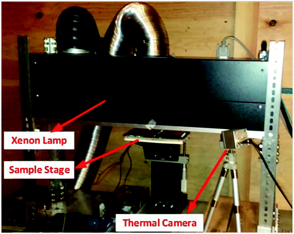 | ||
| Fig. 1 Experimental setup of IPL used in this work. | ||
Recent work on IPL of spherical silver (Ag) nanoparticles (NPs) has shown a coupling between optical absorption and densification in the deposited NP ensemble.5 Optical absorption by the NPs during IPL increases the ensemble temperature. Temperature driven neck growth between NPs progressively reduces the sharpness of nanoscale geometric features between adjacent NPs, which reduces the magnitude of plasmonic absorption. Consequently, the absorption-induced thermal dissipation per unit film volume reduces till it eventually no longer exceeds conductive and convective losses during an IPL pulse. This results in a turning point in temperature evolution. After this turning point the maximum temperature per pulse reduces and levels off with little additional densification occurring, despite the fact that the input optical energy per pulse is unchanged.9 Therefore, this form of coupling between densification and optical absorption is self-damping in nature, i.e., densification of the film after a certain point inherently inhibits further densification by reducing additional optical absorption. IPL of highly porous metallic nanowire (NW) network films has been used to fabricate flexible and transparent conductive films on polymers.10–12 Optical sintering of such silver nanowire (NW) films has shown a reduction in total absorption efficiency of the film (i.e., absorbed power per unit incident optical power) with the progression of neck growth between adjacent nanowires.13 However, the temperature evolution of the film was not reported. Joo et al.14 fabricated dense conductive films via the addition of 5% by weight Cu NWs to Cu NPs and reduced the post-IPL resistivity to about 13 times that of bulk copper. Since the film temperature during IPL was not measured it is not clear how the processing temperatures, and the coupling between densification and optical absorption, changed due to mixing NWs and NPs. Moreover, this work examined limited ratios of NWs to NPs (0%, 1%, 3%, 5% and 100% by weight) and the aspect of ratio of the NWs was small (150 nm diameter and 1–2 μm in length).
Overall, the state-of-the-art in IPL yields limited information on how the nanomaterial shape distribution, e.g., relative ratio of NWs to spherical NPs, might affect the processing temperatures or the coupling between optical absorption and densification. This work has two goals with respect to IPL of conductive nanomaterials. First, to characterize the influence of nanomaterial shape distribution on processing temperatures and sintered material properties. Second, to understand how nanomaterial shape distribution in the film affects the nature of the coupling between optical absorption and densification.
To achieve these goals, we characterize the temperature evolution during IPL of Ag NW–NP composite films with varying content of NWs (0%, 25%, 50%, 75%, 100% by weight). The electrical, optical and morphological properties of the films are compared. Nanoscale electromagnetic simulations are performed to evaluate optical absorption and the interfaces at which maximum thermal dissipation occurs in model composite NW–NP ensembles with varying ratios of NWs to NPs. The ability of the theoretical findings to explain the experimentally observed temperatures trends is explored. Further, the implications on controlling the degree of coupling between densification and optical absorption and on balancing high throughput, low processing temperatures, and low resistivity with low material costs is discussed.
Methods
Experimental methods
Commercially obtained Ag NPs of average diameter 40 nm ± 10 nm (US Research Nanomaterial) and NWs of average diameter 40 nm ± 20 nm and length 100–200 μm (ACS Materials) were mixed in ethanol without any dispersant. Ag nanomaterials were chosen here since sintering of this material is commonly used in fabrication of rigid and flexible electronics.3–5,15 The ratio of NWs to NPs was varied from 0% to 100% in steps of 25% by weight (Table 1). The resulting concentration of Ag nanomaterial in the solution was less than 5% by weight for all cases. After ultrasonication for an hour the inks were found to be stable for at least one hour. During this time period, the inks were deposited onto 25 mm by 15 mm glass substrates via a home-made wide-area aerosol spray system. A magnetic mixer was used within the ink delivery syringe to minimize agglomeration of the NPs and NWs in the suspension. The height of the printer head above the substrate and the ink flow rate were fixed at 12 mm and 1.5 ml min−1 respectively, and the air pressure to the aerosol jet head was fixed at 0.5 psi. The printhead translation speed and the number of deposition passes were varied for different NW content (as in Table 1) to retain similar thickness of the deposited film independent of the NW content. The deposited films were dried at room temperature in air for 5 minutes. The as-deposited film thickness, measured using a ZeScope white light interferometer (resolution 300 nm), is shown in Table 1.| NW to NP ratio (% by weight) | Printhead translation speed (mm min−1) | No. of printing passes | As-deposited film thickness (μm) |
|---|---|---|---|
| 0 | 1400 | 2 | 4.32 ± 0.27 |
| 25 | 1400 | 2 | 4.46 ± 0.39 |
| 50 | 1200 | 2 | 4.42 ± 0.41 |
| 75 | 1200 | 4 | 4.36 ± 0.47 |
| 100 | 1200 | 4 | 4.35 ± 0.45 |
IPL of the films was performed using a Sinteron 3000 system (Xenon Corporation) with the lamp energy primarily lying within the 400–700 nm wavelength range. This system (Fig. 1) consists of a pulsed linear xenon lamp with a reflector that focusses light to a rectangular optical footprint. The on-time ton (in microseconds) and the lamp voltage V (in volts) are used to control the optical energy per pulse Ep as per the relationship Ep = (V/3120)2.4 × ton. For all experiments performed here the V and ton were fixed at 3 kV and 1275 microseconds respectively. The as-deposited films were placed on a borosilicate glass slab on a sample holder platform (Fig. 1), which was mounted onto a micrometer stage, such that the film surface was at 1 inch from the lamp (i.e., at focal point). Since the optical footprint of the xenon lamp light at this location is 12 inches by 0.75 inches the pulse fluence at the film surface was 20 J cm−2. This method for calculation of the optical power was further confirmed by experimental measurement of optical power using a Gamma Scientific S471 optometer that had a nearly 95% relative response within a 400–700 nm wavelength range. The samples were exposed to 3 and 6 pulses of light and at least 5 experiments were conducted for each combination of pulse number and NW content of the film. A thermal camera (MicroEpsilon thermoimager TIM 200, maximum temperature 1500 °C, error ± 2%) was used to measure the evolution of film temperature during IPL. The camera was placed such that the entire surface of the film was visible to it during IPL (Fig. 1). The emissivity of the films, at this fixed camera position, was manually calibrated within this IPL setup by heating the sample and glass slab to 80 °C on a hot plate till the Ag film reached a steady state temperature.
Sheet resistance was measured using a Signatone four-point probe over at least 3 locations per sample. The average bulk resistivity was calculated using the average thickness and the average sheet resistance. The standard deviation in bulk resistivity was obtained using the average thickness and the measured standard deviation in sheet resistance. Film morphology was characterized using Scanning Electron Microscopy (SEM) with a FEI Quanta 3D dual beam system. The crystallinity of the film was characterized via X-ray diffraction (XRD) using a Rigaku Ultima-IV X-ray diffractometer in the Bragg–Brentano configuration with a resolution of 2θ = 0.05°.
The percentage transmittance T and reflectance R were measured using a JASCO V670 spectrophotometer equipped with an integrating sphere. The percentage absorptance A was obtained as A = 100 − T − R. The motivation for optical characterization of the films was to characterize the change in absorption of the xenon lamp light by the film as neck growth and shrinkage occurred in the film. Thus, the optical measurements were confined to 400–700 nm wavelengths, i.e., within which most of the xenon lamp power lies.
Computational methods
The goal of the modeling effort is to qualitatively understand how the change in NW content in a mixed NW–NP ensemble alters the coupling between densification and optical absorption in IPL. Four geometric compositions of the NW–NP ensemble were considered with progressively increasing NW content relative to NP content, i.e., only NPs (unsintered case in Fig. 2A), 2 NWs–9 NPs (unsintered case in Fig. 2B), 2 NWs–4 NPs (unsintered case in Fig. 2C) and only NWs (unsintered case in Fig. 2D). The diameter of each NP and NW was 40 nm. Past work has modeled optical absorption in NW ensembles using NWs with smaller length than in experiments, but with sufficient length to capture the region of electromagnetic coupling at the NW–NW interface.13,16 This approach overcomes the infeasibly high computational time for electromagnetic modeling of nanomaterials that have one dimension in micrometers (length of NW) and the other in nanometers (diameter of NW). Based on this reasoning, the length of each NW was fixed at 120 nm in this modeling effort.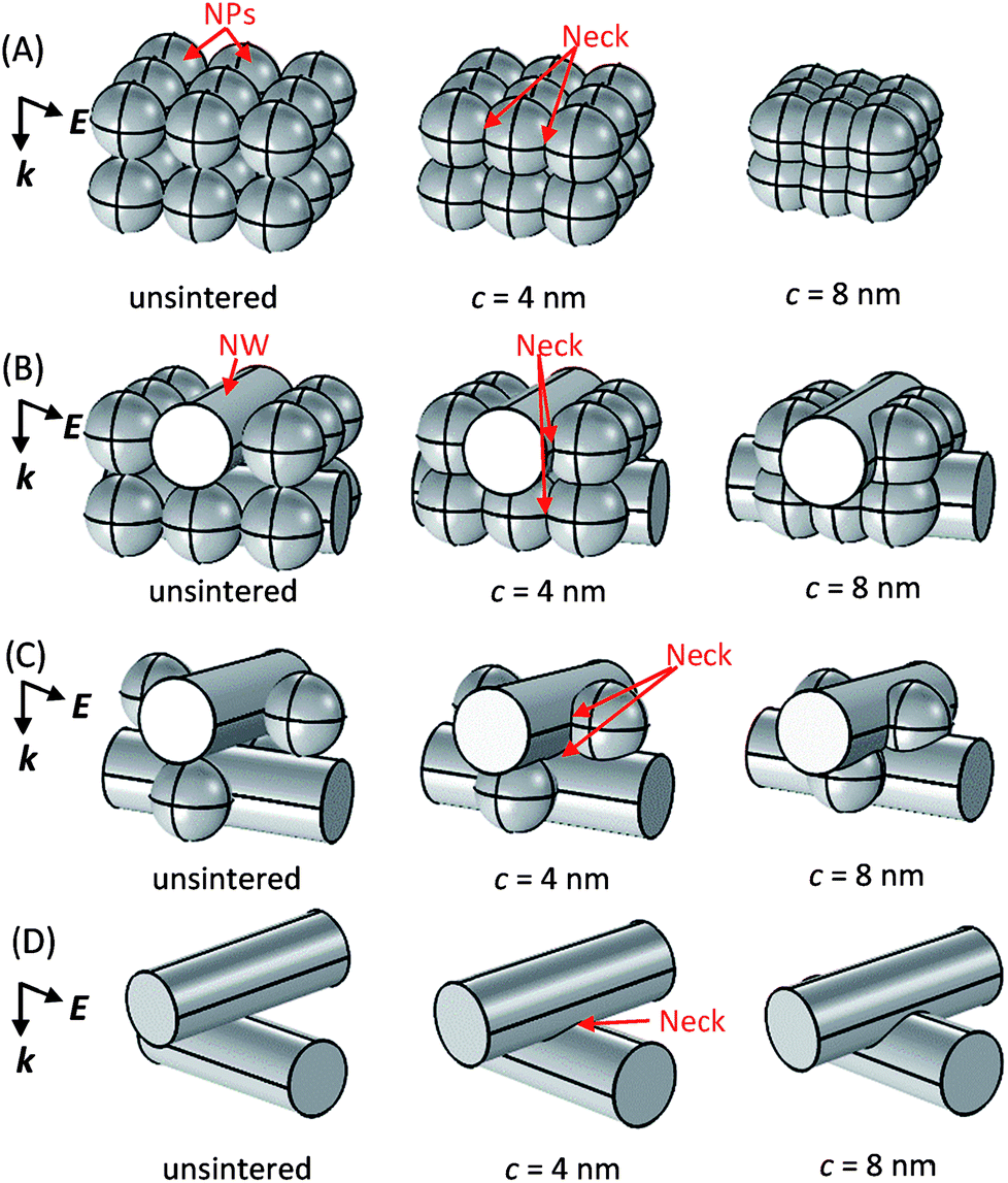 | ||
| Fig. 2 Schematic of modelled ensembles consisting of (A) only nanoparticles (B) 2 nanowires and 9 nanoparticles (C) 2 nanowires and 4 nanoparticles (D) only nanowires. | ||
The geometric parameter c (Fig. 3A–C) between adjacent NPs and NWs was parametrized at 2 nm, 4 nm, 6 nm and 8 nm to obtain sintered ensemble geometries. Examples of sintered ensemble geometries for c = 4 nm and 8 nm are shown in Fig. 2.
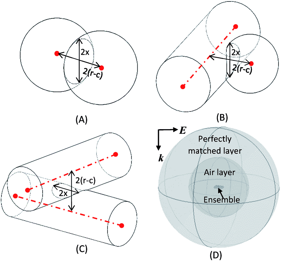 | ||
| Fig. 3 Schematic of geometric parameter c between adjacent (A) nanoparticles (B) nanoparticle and nanowire (C) nanowires. r = 20 nm is radius, red dots show centres of nanoparticles and dotted lines show axes of nanowires. (D) Schematic of model used for electromagnetic simulations in COMSOL. | ||
Fig. 3A–C show that greater c implies a reduction in interparticle center-to-center distance 2(r − c), where r is the nanomaterial radius. The center-to-center distance 2L = 2(r − c) represents shrinkage between adjacent particles.17,18 Denoting the corresponding neck diameter by 2x (Fig. 3A–C), the relationship (x/r)2 = 1 − (L/r)2 relates the corresponding neck size to the shrinkage.19
Therefore, a reduction in L (greater shrinkage) due to an increase in c implies an increase in x. This allows c to be used as a geometric parameter for creating NW–NP ensemble geometries with increasing shrinkage and neck size. Note that for NWs and NPs of this diameter, while surface diffusion might be present, interparticle neck growth is likely to be dominated by bulk diffusion mechanisms such as grain boundary and volume diffusion rather than by surface diffusion.18
The assumption of uniform c in an ensemble irrespective of the interface type (i.e., NP–NP, NP–NW or NW–NW contact) assumes equal shrinkage and neck growth in all the geometric compositions independent of NW content. The sintered and unsintered ensembles were placed in a spherical air shell and surrounded by a perfectly matched layer to prevent spurious reflections (Fig. 3D). A unit electric field linearly polarized along E and travelling along k was incident on the ensemble (Fig. 2 and 3D). The electric field polarization was perpendicular to the axis of the top layer NW to maximize the coupling of the optical field into the ensemble, after Garnett et al.13 The wavelength-dependent real and imaginary dielectric constants of Ag were obtained via the Drude–Lorentz model.20 The mesh sizes, size of air shell and size of the perfectly matched layer were refined till their effect on the predicted absorption and scattering curves was negligible. The electromagnetic simulations were conducted in COMSOL over the 400–700 nm spectrum in steps of 20 nm.
While neck growth and shrinkage between adjacent NPs and NWs might be different there are little reports in literature of how different they might be quantitatively. We also use NW–NP ensemble geometries in which, in a qualitative analogue to the experiments, the ratio of number of NWs to NPs changes. However, since the weight ratio of NWs to NPs in these models does not quantitatively replicate the weight ratios in experiments the predicted absorption is expected to mirror experimental observations in a purely qualitative rather than a quantitative sense. The inability to use quantitatively predictive models arises from the fact that such models would require implicit linking of densification, electromagnetic coupling, and thermal transfer in large 3D ensembles of nanomaterials. Currently, these individual modeling components for large 3D ensembles of nanomaterials with different shapes are still an active area of research. At the same time, our approach does allow qualitative insight into experimental observations. Further, this nanoscale electromagnetic modeling approach will be an essential building block of more detailed multiphysical models, as was recently done for IPL of purely spherical nanoparticle films.5,9
Results and discussion
Experimental results
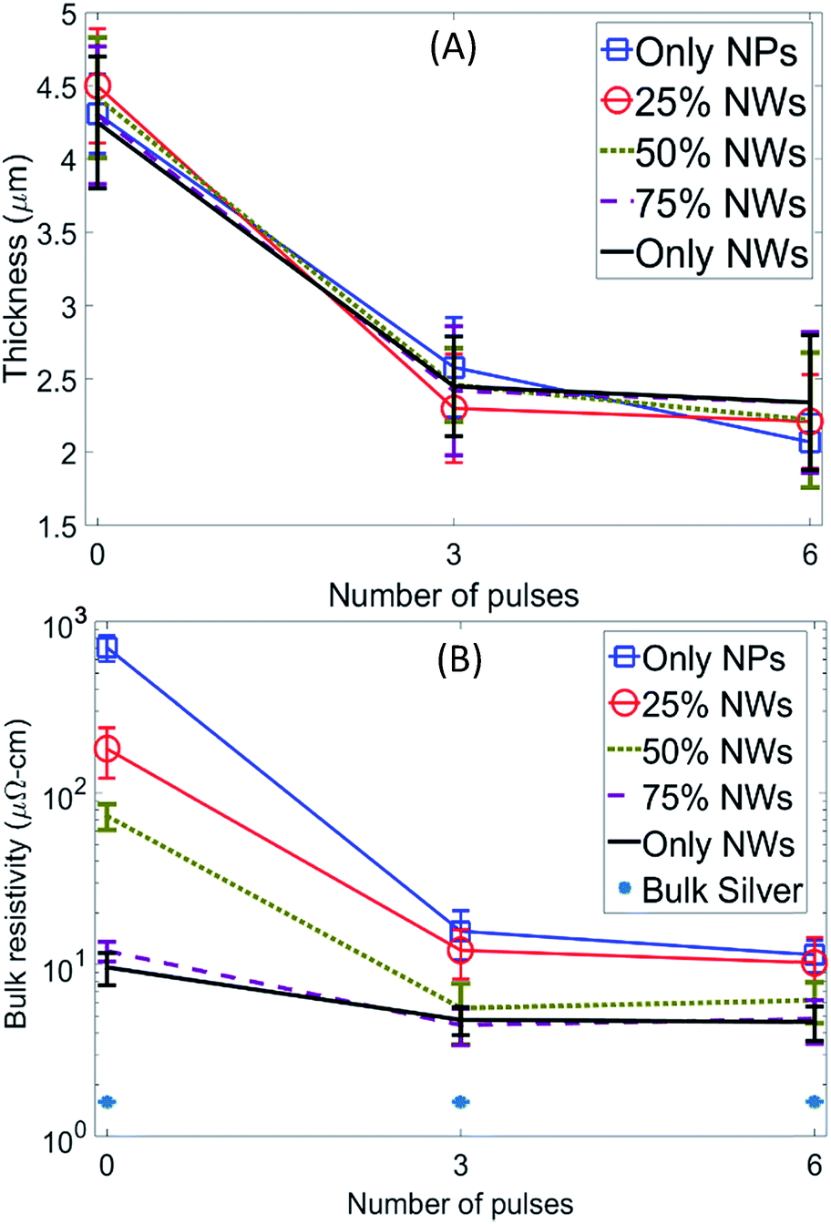
Fig. 4A to E show representative plots of experimentally measured temperature evolution during IPL. Fig. 4F shows the average of the peak temperature in each pulse with the standard deviation represented by error bars. The peak temperature in the first pulse is highest for the 0% NW (NP only) case and decreases progressively with increasing NW content of the film. The maximum film temperature for the 0% NW film is around 235 °C and reduces to around 150 °C as the NW content increases to 50% by weight or greater. For the 0% NW film, there is a significant drop in peak pulse temperature from the first to the second pulse. At a higher NW content of 25% the temperature drop after the first pulse is relatively lower. As NW content increases to 50% and above there is a progressive reduction in the temperature drop from first to second pulse.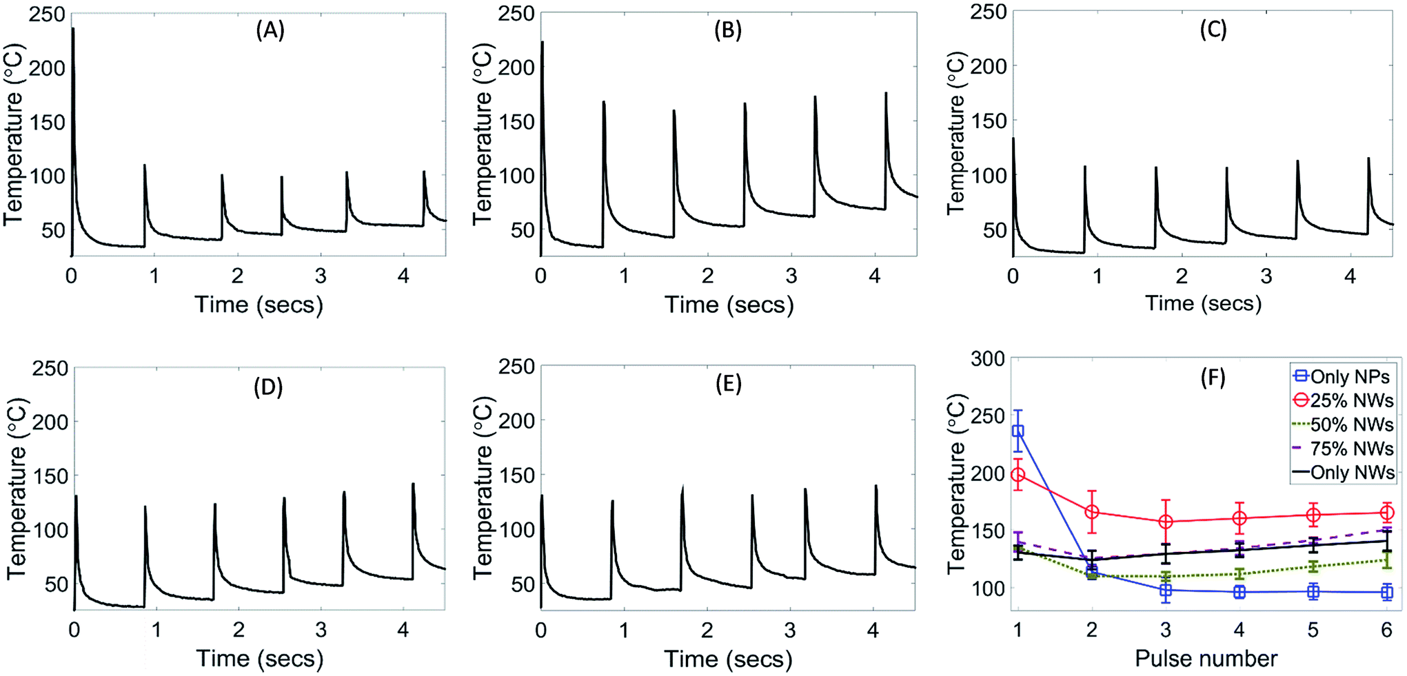 | ||
| Fig. 4 Representative temperature evolution curves for films with (A) 0% nanowires, i.e., only nanoparticles (B) 25% nanowires (C) 50% nanowires (D) 75% nanowires (E) 100% nanowires, i.e., only nanowires; (F) peak pulse temperature as a function of nanowire content of the film. | ||
Another interesting observation from Fig. 4F is the evolution of peak pulse temperature after the drop in the second pulse. For 0% NW content the peak pulse temperature levels off after the initial drop in the second pulse. For 25% NW content the maximum pulse temperature seems to rise back again after the third pulse, although by a statistically insignificant amount. However, for films with 50% NW content and above there is a more appreciable rise in temperature after the initial temperature drop.
Note that the above temperature trends are despite no change in incident lamp power in consecutive pulses. The drop in temperature after the first pulse and levelling off of temperature after the second pulse for the 0% NW film has been observed previously,9 and explained via the self-damping coupling described in the introduction section. However, since only the 0% NW films were studied these works cannot explain the observed change in temperature evolution for NW content greater than 0%. Fig. 5A shows that the film thickness reduces by about half after IPL for all NW contents, indicating that the film shrinkage is independent of the NW content. The bulk resistivity (Fig. 5B) of the as-deposited film reduces as the NW content of the film increases, and reduces after IPL as well, as expected.3,4,15,21 For 50% NW content, the average bulk resistivity after IPL (i.e., number of pulses >0 in Fig. 5B) is 7.8 μΩ cm, i.e. about 5 times that of bulk silver.3 For 75% and 100% NW content the average post-IPL bulk resistivity is 6.9 μΩ cm, i.e., about 4.3 times that of bulk silver.
 | ||
| Fig. 5 (A) Film thickness (B) bulk resistivity as a function of number of pulses and nanowire content of the film. 0 pulses indicate as-deposited film. | ||
The temperature evolution curves in Fig. 4F show that for 50%, 75% and 100% NW content the maximum processing temperature is around 150 °C. Thus, a bulk resistivity between 4–5 times that of bulk silver is obtained with a peak processing temperature of around 150 °C in these experiments. Fig. 5B also shows that increasing the NW content from 0% to 100% results in progressively lesser reduction in resistivity of the post-IPL films as compared to the corresponding as-deposited film (0 pulses in Fig. 5B). Since reduction in resistivity is primarily controlled by neck growth between the NWs and NPs,22 the above observation indicates that interparticle neck growth due to IPL is also progressively reducing as the NW content increases from 0% to 100%. Fig. 5 also shows that there is little change in shrinkage or resistivity from 3 to 6 pulses.
These results enable a qualitative assessment of change in bulk diffusion (grain boundary and volume diffusion combined) and surface diffusion as a function of the NW content of the film, albeit without allowing a quantitative comparison between magnitudes of surface and bulk diffusion for a given NW content. This is based on the following observations. Shrinkage between nanomaterials is primarily due to bulk diffusion, with no contribution from surface diffusion.17,18,23 The similar degree of shrinkage observed here (Fig. 5A) for different NW contents of the film indicates that the bulk diffusion in these experiments does not depend significantly on the NW content of the film. Reduction in resistivity is related to neck growth between particles,22 which can occur due to both bulk and surface diffusion.17,18,23
The lesser reduction in post-IPL resistivity relative to the corresponding as-deposited film, with an increase in NW content (Fig. 5B), while retaining similar shrinkage (Fig. 5A) implies that in these experiments surface diffusion becomes progressively less active as NW content increases but bulk diffusion is independent of NW content. While these observations do not allow direct quantitative comparison of the degrees of grain boundary, volume and surface diffusion for a given NW content we note that for NWs and NPs of this diameter interparticle neck growth is typically dominated by bulk diffusion rather than by surface diffusion.18
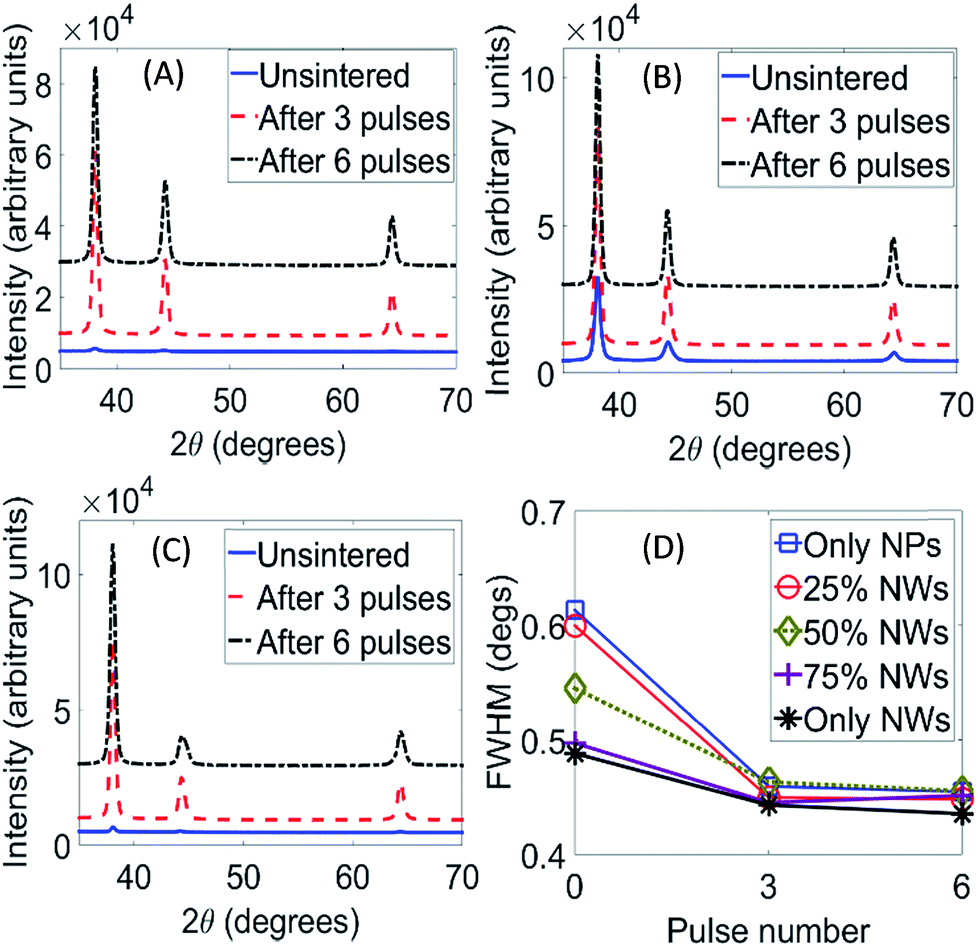
The measured X-ray diffraction spectra (representative example in Fig. 6A–C) show sharp peaks at 2θ = 38.24, 44.42, 64.44° which can be ascribed to the (111), (200) and (220) peaks of FCC silver (JCPDS card 04-0783). Additional spectra are shown in Fig. S1 (ESI†).
 | ||
| Fig. 6 XRD spectra of unsintered and sintered films for (A) 0% nanowire film (B) 50% nanowire film (C) 100% nanowire film, all offset along intensity axis for clarity (D) FWHM of the (111) peak as a function of pulse number and nanowire content. 0 pulses indicates as-deposited film. | ||
Fig. 6D shows that for 0% to 100% NW content the FWHM of the major (111) peak reduces after IPL, indicating a general increase in crystallite size due to sintering. We also observe that the quantitative degree of this reduction in FWHM as compared to the as-deposited film (0 pulses in Fig. 6D) changes with the NW content of the film. As the NW content increases from 0% (only NPs) through 25%, 50% and 75% (mixed NW–NP) to 100% (only NWs) the reduction in FWHM relative to the corresponding as-deposited film becomes progressively lesser. Thus, crystallite growth due to IPL reduces as NW content increases.
This supports the observation (Fig. 5B) that the degree of sintering decreases with greater NW content. This might be because the maximum film temperatures are greater for lesser NW content (Fig. 4), due to quantitatively different atomic diffusion with increasing NW content of the film, or a combination of both. Fig. 6D also shows that crystallite growth tapers off after 3 pulses which supports the observation in Fig. 5 that there is little additional sintering after three pulses.
Fig. 7 shows SEM images of the unsintered and sintered films. For the 0% NW film, there is neck growth and enlargement in particle size due to coalescence of particles during IPL (Fig. 7A–C). At 25% NW content (Fig. 7D–F) the surface morphology of the NWs is largely retained after IPL, while the NPs bond to each other and enclose the NWs within. For 50% (Fig. 7G–I) and 75% (Fig. 7J–L) NW content there is greater change in the post-IPL NW surface morphology. Localized reduction and increase in NW diameter can be observed due to coalescence of NPs with each other and into the surface of the NWs. For 100% NW content (Fig. 7M–O) the post-IPL NWs show a localized diameter reduction at various points along the NW length which might be due to diffusion along the length of the NWs,24 but cannot be conclusively confirmed. Larger scale SEM images are shown in Fig. S2 in (ESI†).
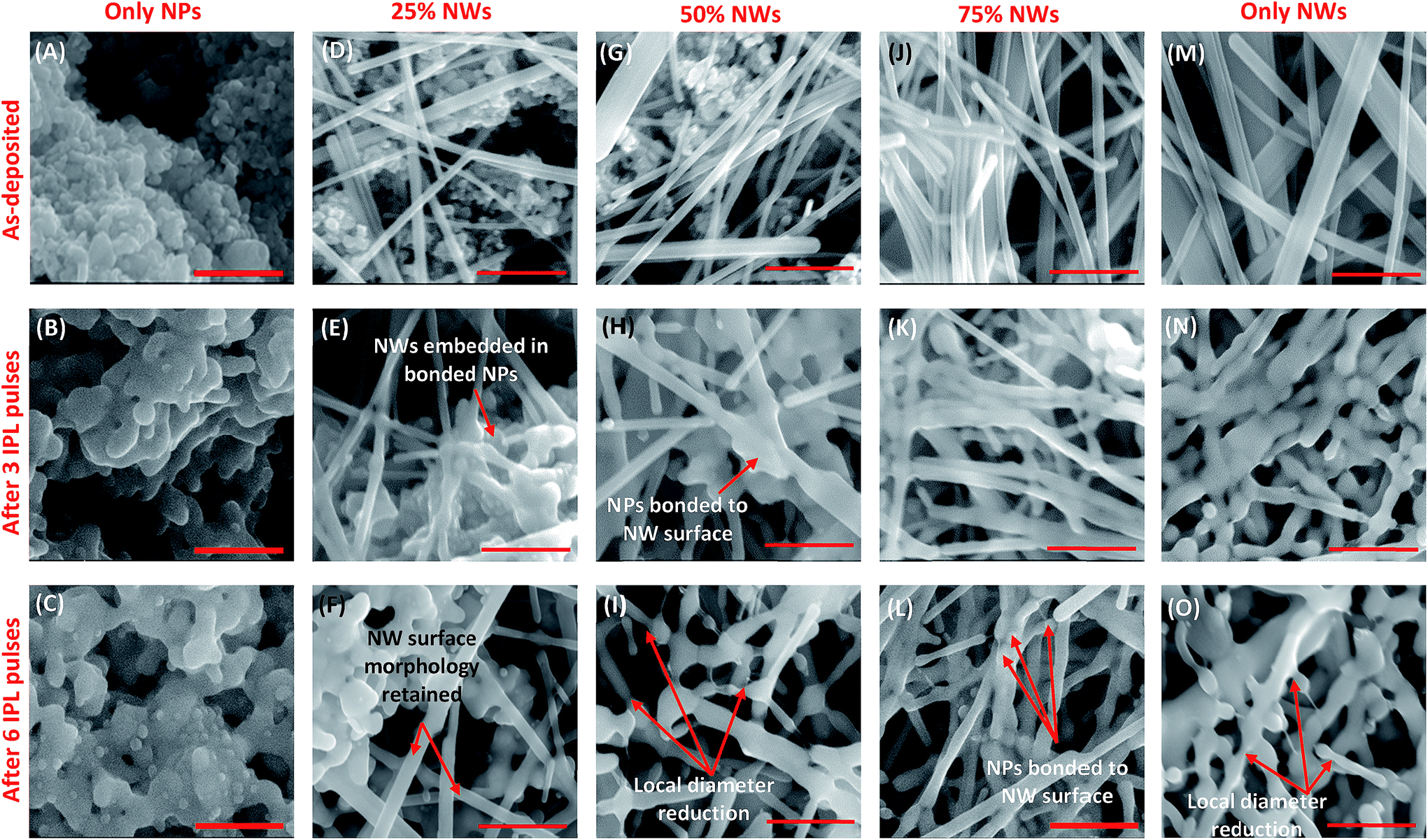 | ||
| Fig. 7 SEM images of unsintered and sintered films for different number of IPL pulses and different nanowire content. Scale bar corresponds to 500 nm length. | ||
Fig. 8A–E compare optical absorption by the film before and after IPL. The transmittance of the film was zero due to the significant film thickness, so that the absorptance percentage was obtained from the reflectance data only (Fig. S3, ESI†). Absorption by the unsintered film is greatest for 0% NW content and reduces with greater NW content of the film. So, at the beginning of the first pulse the heat source that drives temperature rise and densification in the film reduces as NW content increases.
 | ||
| Fig. 8 Optical absorption spectra for film consisting of (A) 0% nanowires (B) 25% nanowires (C) 50% nanowires (D) 75% nanowires (E) 100% NWs; (F) normalized cumulative absorption as a function of nanowire content and number of pulses. 0 pulses indicates as-deposited film. | ||
Therefore, peak temperature in the first pulse progressively reduces with increasing NW content (Fig. 4F). The cumulative absorption was obtained from these optical spectra, and for each NW content case these cumulative absorptions were divided by that of the corresponding as-deposited film to obtain a normalized total absorption (Fig. 8F). Since the as-deposited film has greater absorption than the sintered films for all the cases examined here, the normalized absorption for the as-deposited films was therefore 1. The reduction in absorption after IPL is the greatest for the 0% NW case and reduces as the NW content of the film increases. This explains why the drop in temperature from the first to second IPL pulse is greatest when the NW content is the lowest (Fig. 4F). Further note that the optical absorption drops after 3 pulses and then levels off for all cases. As shown in previous work5,9 this saturation in optical absorption after a certain number of pulses is because sintering results in reduction in nanoscale features in the films, thus reducing plasmonic absorption of visible light by the film in subsequent pulses.
A key question is, why is the reduction in optical absorption from unsintered film to 3 IPL pulses different for different NW contents of the film? The reduction in optical absorption in IPL of 0% NW films (also seen here) has been attributed to the loss of nanoscale geometric features in the film due to progression of sintering,9 which inhibits additional sintering. This could explain why optical absorption and densification level off after 3 pulses. In our experiments, the degree of densification reduces with greater NW content of the film (Fig. 4–6), i.e., loss of nanoscale features is lesser when the NW content is higher. It could be thought that this is the only reason why the drop in optical absorption is lesser for greater NW content, which is also why the temperature drop in the second pulse is lesser for greater NW content. However, since the degree of sintering is unequal for different NW content of the film the experimental observations cannot conclude if there is an inherent effect of NW content on the coupling between optical absorption and densification in IPL. The next section describes results from electromagnetic models, which enforce uniform sintering (via equal parameter c at all interparticle contacts, Fig. 3A–C) to overcome the above issue.
Computational results
Fig. 9 shows representative contours of predicted thermal power dissipation density at 400 nm for different geometric compositions corresponding to c = 0 nm and 4 nm. For the only NPs case in the unsintered state (Fig. 9A) the dissipated power density is the greatest along E at the initial point of contact between two adjacent NPs in the top layer.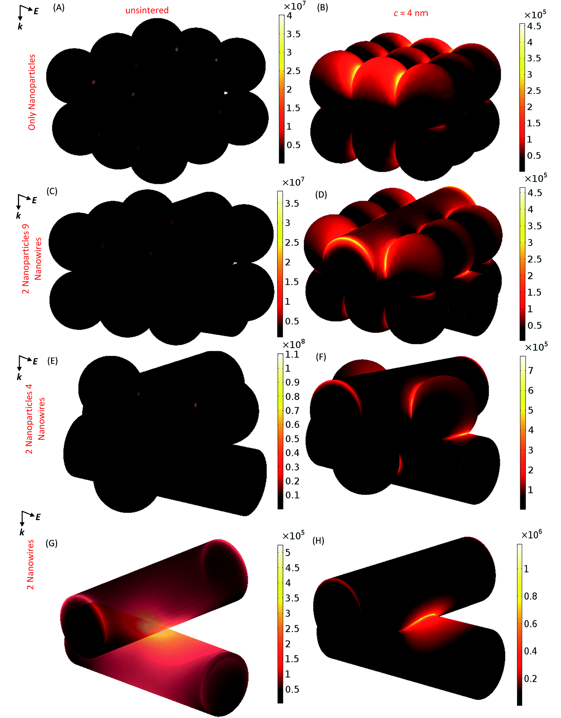 | ||
| Fig. 9 Contours of thermal power dissipated per unit volume of solid material (in W m−3) at 400 nm under a unit incident electric field. Images not to geometric scale. | ||
With the progression of necking (Fig. 9B) the point of maximum thermal dissipation (still in the top NP layer) moves with the neck interfaces away from the initial point of contact. This phenomenon has been shown in past work as well.9,16 In the unsintered 2 NW–9 NPs case (Fig. 9C) the maximum dissipation density is again in the top layer at the interface between the NPs and NWs. In the sintered state (Fig. 9D) additional locations of non-negligible dissipation density can be observed. In addition to the NP–NW interfaces in the top layer at which necks are formed there is also significant thermal dissipation at the ends of the top layer NW and at the interface between the top layer NPs and the bottom layer NW. As the NW content is increased even further in the 2 NW–4 NP case we again observe these additional locations of maximum dissipation density after sintering (Fig. 9E and F). Note that the dissipation density at the interface between the NWs is negligible in both 2 NW–9 NP case and in 2 NW–4 NP case. For the only NW case, the dissipation density in the unsintered state (Fig. 9G) is maximum at the point of contact between the NWs and again moves with the neck as it develops (Fig. 9H). Thus, when NWs and NPs are mixed together the interparticle interfaces (NP–NP, NP–NW and NW–NW) at which maximum thermal dissipation occurs changes with sintering. Note that the influence on optical absorption, of fusion of NPs with each other and with NWs in NW–NP mixtures (Fig. 7G–L), is captured via the fusion of the NPs into the NWs and with each other in the 2 NW–9 NP and 2 NW–4 NP geometries (Fig. 9D, F and S4 in (ESI†)).
Integrating the dissipated power density over the solid volume of the ensemble at each wavelength yields the dissipated thermal power as a function of wavelength for each geometric composition and c, as shown in Fig. S5 (ESI†). These predicted spectra qualitatively capture the experimentally observed dependence of absorption on wavelength, with greater absorption occurring at shorter wavelengths. Using analytical curve fitting this absorption spectrum was summed over 400–700 nm to yield the total thermal power dissipated in each ensemble. Fig. 10A shows this total dissipated thermal power normalized with respect to the maximum for each combination of geometric composition and c value. The total optical power absorbed and dissipated as heat reduces after sintering, and this drop in absorption reduces with increasing NW content of the ensemble. These trends are also observed from experiments, as described previously (Fig. 4–8). Thus, this model qualitatively captures the experimentally observed trends, in terms of the concurrent dependence of optical absorption on NW content and neck growth in the film. Note that the capability of this model to capture the tapering off in absorption after 3 pulses, as seen in Fig. 8F, is difficult to determine. This is because the degree of sintering observed experimentally differs for different NW content (Fig. 5B), and because quantitative values of solid volume fraction of the film that may be related to parameter c are not easily found from experiments.
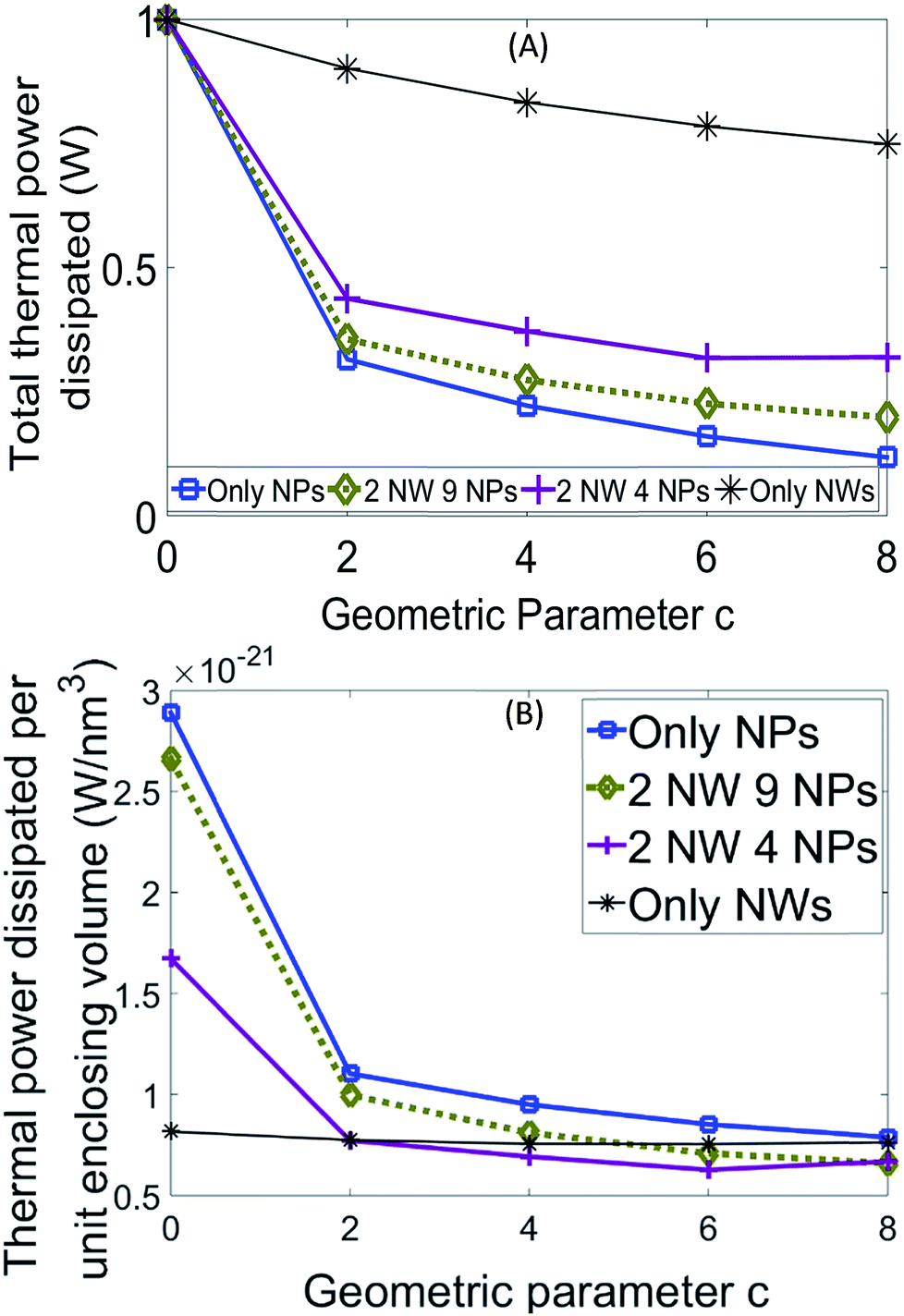 | ||
| Fig. 10 (A) Total thermal power dissipated for the ensembles (B) thermal power dissipated per unit enclosed volume of the ensemble. Shown for 1 V m−1 incident electric field. c = 0 indicates unsintered ensemble. | ||
Given the high thermal conductivity of silver and the relatively small film thickness, the heat transfer in the film can be described by the lumped capacitance model shown in eqn (1).9
| Q = (ρC)effT + Qconv + Qcond | (1) |
In this model the rate of change of film temperature T depends on the thermal power dissipated per unit volume of the film Q, the effective volumetric heat capacity of the film (ρC)eff, convective thermal power lost per unit volume of film Qconv, and conductive thermal power lost per unit volume of film Qcond. Note that the volume of the film here includes both the volume of the solid Ag material and the pores in the film. The (ρC)eff in turn depends on the solid volume fraction of the film θ, and the density and specific heat capacity of silver (ρAg,CAg) and of the air in the pores (ρAir,CAir), as shown in eqn (2).
| (ρC)eff = ρAgCAgθ + ρAirCAir(1 − θ) | (2) |
As shown in previous work5,9 it is the evolution of Q with sintering (or θ) that dominates the evolution of film temperature. Greater Q of the as-deposited material results in greater temperature rise before onset of sintering. The extent by which Q reduces or increases with the evolution of sintering dictates the extent to which the film temperature reduces or increases during consecutive IPL pulses. For the computational model developed here, the Q for each combination of geometric composition and c is the thermal power dissipated (Fig. 10A) per unit volume of the smallest box enclosing the ensemble.
As shown in Fig. 10B, the magnitude and evolution of Q depends significantly on the NW content of the ensemble. As the relative NW content is increased, from only NPs case to 2 NW–9 NP case to 2 NW–4 NPs case and then only NWs case, the Q for the as-deposited material (c = 0) progressively reduces. This is reflected in the experimental observation (Fig. 4F) that the maximum temperature during the first pulse of IPL (corresponding to IPL of the unsintered material) reduces with increasing NW content.
Further, as the NW content of the ensemble changes the degree of dependence of Q on densification also changes. For the only NPs ensemble, there is a significant drop in Q at c = 2 nm and beyond c = 2 nm the additional drop is lesser but Q still monotonically reduces. As the NW content increases (cases corresponding to 2 NWs with 9 NPs and 4 NPs in Fig. 10B) the drop in Q from c = 0 to 2 nm is progressively lesser and Q does not drop as fast. For the only NWs case, the drop in Q is insignificant as compared to the above cases. This implies that as densification proceeds the films with greater NW content retain the as-deposited levels of optical absorption to a greater extent. This allows optical absorption to keep pace with convective and conductive losses and is reflected in the experimental observation that as the NW content of the film increases there is an increase in temperature following the drop in the second pulse (50% and 75% NW content in Fig. 4F), with almost no drop being observed for a film with only NWs (only NWs case in Fig. 4F).
To summarize, there is an inherent dependence of the degree of coupling between densification and optical absorption on the relative content of NWs to NPs in the film. Our previous work5,9 has shown that densification during IPL of only NP films reduces optical absorption per unit film volume resulting in a significant turning point in temperature, i.e., a self-damping coupling which is also seen in this work (Fig. 4F and 10B). Based on the electromagnetic modelling performed here the degree of this self-damping coupling depends inherently on the nanomaterial shape distribution (ratio of NWs to NPs here). As the NW content increases the degree of this self-damping behaviour reduces, till a point is reached where the initial drop in temperature is barely perceptible (e.g., only NW film in Fig. 4F). This implies that there is an inherent effect of mixing nanomaterials of different shapes together on the coupling behaviour in IPL, which influences temperature evolution and thus densification during IPL. Another interesting observation is that for only NPs (Fig. 9A and B) and only NWs (Fig. 9G and H) cases the specific interparticle interfaces at which maximum thermal dissipation occurs stay the same after sintering as they were before sintering. However, when NWs and NPs are mixed together (Fig. 9C–F) there is a change in the specific interparticle interfaces at which maximum thermal dissipation occurs upon sintering.
Conclusions
This work examines the effect of nanomaterial shape distribution in silver NW–NP composite films on sintering temperatures and sintered material properties in IPL, yielding the following insights and implications on process performance and material properties.Mixing nanowires with nanoparticles can reduce the maximum sintering temperatures to around 150 °C (Fig. 4F), while retaining film resistivity within 4–5 times that of bulk silver (Fig. 5B). Since the shrinkage (Fig. 5A), resistivity (Fig. 5B) and XRD data (Fig. 6D) show little additional sintering or change in bulk resistivity beyond 3 pulses, the above properties can be obtained within 2.5 seconds of processing time. This has significant implications on reducing substrate distortion and damage when using thermally sensitive substrates like polymers and paper, without compromising on process throughput or sintered material conductivity.
Since NWs are typically 2–3 times more expensive than NPs, there is an optimum NW content that can balance low material costs with the above process performance and sintered material resistivity. For example, in our experiments for NW content of 50% or greater the maximum film temperature is 150 °C while retaining the above process throughput and film resistivity (Fig. 4F and 5B). So, based on these experiments choosing a NW content of 50% will minimize materials cost while retaining the low processing temperatures, high processing speed and low film resistivity achieved here.
The performed electromagnetic simulations show an inherent dependence of the coupling behaviour in IPL on the nanomaterial shape distribution in the as-deposited film. This certainly influences temperature evolution and therefore densification during the process, and is reflected in the experimentally observed dependence of degree of sintering and change in resistivity after IPL on the NW content of the film. These observations hint at the potential for mixing additional nanomaterial shapes (e.g., nanoflakes) with NWs or NPs to control the processing temperature in IPL, by tailoring the as-deposited material absorption and the coupling between optical absorption and densification. Experimental efforts to explore this possibility are currently underway.
Theoretically, there is a need for extension of electromagnetic models (such as the one shown here) to account for random nanomaterial packing. These models must be linked to mesoscale models of densification and heat transfer to quantitatively understand and predict the dependence of coupled optical-thermal-mass transfer phenomena on nanomaterial shape distribution. The observed dependence of volumetric absorption on a combination of nanomaterial shape distribution and densification will be a critical component of such theoretical models. Further, the dependence of the above coupling behaviour on the material type and composition also needs to be investigated. This is a topic of future work by the authors.
Conflicts of interest
There are no conflicts to declare.Acknowledgements
The authors gratefully acknowledge the support for this work by the National Science Foundation, USA, grants CMMI #1537196 and CBET #1449383.References
- H.-S. Kim, S. R. Dhage, D.-E. Shim and H. T. Hahn, Appl. Phys. A: Mater. Sci. Process., 2009, 97, 791–798 CrossRef CAS.
- M. Jha, R. Dharmadasa, G. L. Draper, A. Sherehiy, G. Sumanasekera, D. Amos and T. Druffel, Nanotechnology, 2015, 26, 175601 CrossRef CAS PubMed.
- J. S. Kang, J. Ryu, H. S. Kim and H. T. Hahn, J. Electron. Mater., 2011, 40, 2268–2277 CrossRef CAS.
- C. Wan-Ho, H. Hyun-Jun, L. Seung-Hyun and K. Hak-Sung, Nanotechnology, 2013, 24, 035202 CrossRef PubMed.
- W. MacNeill, C.-H. Choi, C.-H. Chang and R. Malhotra, Sci. Rep., 2015, 5, 14845 CrossRef CAS PubMed.
- S.-H. Park and H.-S. Kim, Thin Solid Films, 2014, 550, 575–581 CrossRef CAS.
- S. R. Dhage and H. Thomas Hahn, J. Phys. Chem. Solids, 2010, 71, 1480–1483 CrossRef CAS.
- R. Dharmadasa, B. Lavery, I. M. Dharmadasa and T. Druffel, ACS Appl. Mater. Interfaces, 2014, 6, 5034–5040 CAS.
- S. Bansal and R. Malhotra, Nanotechnology, 2016, 27, 495602 CrossRef CAS PubMed.
- K. Mallikarjuna, H.-J. Hwang, W.-H. Chung and H.-S. Kim, RSC Adv., 2016, 6, 4770–4779 RSC.
- J. Jiu, M. Nogi, T. Sugahara, T. Tokuno, T. Araki, N. Komoda, K. Suganuma, H. Uchida and K. Shinozaki, J. Mater. Chem., 2012, 22, 23561–23567 RSC.
- J. Jiu, T. Sugahara, M. Nogi, T. Araki, K. Suganuma, H. Uchida and K. Shinozaki, Nanoscale, 2013, 5, 11820–11828 RSC.
- E. C. Garnett, W. Cai, J. J. Cha, F. Mahmood, S. T. Connor, M. Greyson Christoforo, Y. Cui, M. D. McGehee and M. L. Brongersma, Nat. Mater., 2012, 11, 241–249 CrossRef CAS PubMed.
- S.-J. Joo, S.-H. Park, C.-J. Moon and H.-S. Kim, ACS Appl. Mater. Interfaces, 2015, 7, 5674–5684 CAS.
- M. T. Rahman, J. McCloy, C. V. Ramana and R. Panat, J. Appl. Phys., 2016, 120, 075305 CrossRef.
- G. Baffou and R. Quidant, Laser Photonics Rev., 2013, 7, 171–187 CrossRef CAS.
- R. German, Sintering: From Empirical Observations to Scientific Principles, Butterworth-Heinemann, 1st edn, 2014 Search PubMed.
- R. Castro, in Sintering: Mechanisms of Convention Nanodensification and Field Assisted Processes, ed. C. H. R. Ricardo and K. van Benthem, Springer, 2013, ch. 2, vol. 1, pp. 17–34 Search PubMed.
- F. Parhami, R. M. McMeeking, A. C. F. Cocks and Z. Suo, Mech. Mater., 1999, 31, 43–61 CrossRef.
- X. Fan, W. Zheng and D. J. Singh, Light: Sci. Appl., 2014, 3, 14 Search PubMed.
- C. Chen, L. Wang, R. Li, G. Jiang, H. Yu and T. Chen, J. Mater. Sci., 2007, 42, 3172–3176 CrossRef CAS.
- Y. Zhang, L. Wu, X. Guo, Y.-G. Jung and J. Zhang, Comput. Mater. Sci., 2016, 125, 105–109 CrossRef CAS.
- F. Li and J. Pan, in Sintering: Mechanisms of Convention Nanodensification and Field Assisted Processes, ed. R. H. R. Castro and K. v. Benthem, Springer, Berlin Heidelberg, 2013, vol. 35, pp. 18–34 Search PubMed.
- T.-B. Song, Y. Chen, C.-H. Chung, Y. Yang, B. Bob, H.-S. Duan, G. Li, K.-N. Tu and Y. Huang, ACS Nano, 2014, 8, 2804–2811 CrossRef CAS PubMed.
Footnote |
| † Electronic supplementary information (ESI) available: X-ray diffraction spectra, scanning electron microscopy images, reflectance spectra, thermal dissipation contours, predicted optical absorption curves. See DOI: 10.1039/c7ra11013h |
| This journal is © The Royal Society of Chemistry 2017 |