DOI:
10.1039/C6RA27190A
(Paper)
RSC Adv., 2017,
7, 11745-11751
Interface engineering of an AlNO/AlGaN/GaN MIS diode induced by PEALD alternate insertion of AlN in Al2O3
Received
23rd November 2016
, Accepted 12th February 2017
First published on 16th February 2017
Abstract
In this paper, AlNO nano-films have been deposited on an AlGaN/GaN heterojunction by alternating growth of AlN and Al2O3 using plasma enhanced atomic layer deposition (PEALD). With optimized AlN layer insertion in Al2O3, the oxygen is effectively blocked from diffusing to the AlGaN surface and the formation of detrimental Ga–O bonds is significantly suppressed. Owing to the negative fixed charges in Al2O3, provided by the incorporated nitrogen, the flat band voltage (Vfb) of the AlNO/AlGaN/GaN metal–insulator–semiconductor (MIS) diode exhibits a positive shift of 1.50 V, compared with the Al2O3/AlGaN/GaN MIS diode. Markedly reduced hysteresis and frequency-dispersion in the C–V characteristics have also been observed at the AlNO/AlGaN interface. Furthermore, the interface states density (Nit) at the AlNO/AlGaN interface has been reduced by one order of magnitude compared with the Nit at the Al2O3/AlGaN interface, and the border traps density (Nbt) near the AlNO/AlGaN interface is also identified to be reduced by the insertion of AlN layers into Al2O3. The PEALD induced optimization of AlNO deposition on the AlGaN/GaN heterojunction provides a pathway to the fabrication of AlGaN/GaN high electron mobility transistors (HEMTs) with low interface trap density.
1. Introduction
AlGaN/GaN high electron mobility transistors (HEMTs) are ideal for high-frequency, high temperature and high-voltage power switching applications, due to their superior material and device properties, such as high breakdown electric field, low on-resistance, high switching frequency and high temperature operation.1–4 However, there remain urgent issues of large gate leakage and current collapse in Schottky-gate HEMTs (S-HEMTs). The current collapse phenomenon is a temporary reduction of drain-current (ID) immediately after the application of both gate stress and drain stress, which will result in prominently lowered output power than expected from the dc characteristics of S-HEMTs.5,6 In addition, the large gate leakage current in GaN-based S-HEMTs will lead to inferior noise characteristics, larger power consumption and smaller capable gate voltage swing.7 In order to address these issues, HEMTs fabricated with a gate dielectric between AlGaN and gate metals, which are referred to as metal–insulator–semiconductor high electron mobility transistors (MIS-HEMTs) have been proposed. High-κ dielectrics such as Al2O3,8,9 HfO2,10 ZrO2 (ref. 11) and Ta2O5 (ref. 12) are of vital importance to MIS-HEMTs, and among the above high-κ dielectrics, Al2O3 has been well accepted as the gate dielectric due to its large band gap (8.7 eV), high breakdown field (5–10 MV cm−1) and relatively high dielectric constant (κ ∼ 9).13–15 However, the dielectric/AlGaN interface presents new challenges in suppressing/reducing the interface states or border traps and obtaining stable device operation. It has been revealed that there exit large amounts of interface traps with long and short emission time constant (τit) at the dielectric/AlGaN interface due to the presence of detrimental Ga–O bonds, leading to the degradation of device performance or reliability problems.16,17 The dynamic capture/emission processing of these interface traps, especially the ones relatively deep (with longer τit) below the AlGaN conduction band may not be in synchrony with the switching gate control signals, resulting in a threshold voltage instability issue.18–20 In order to overcome this problem, Zhu et al. used AlN to replace high-κ oxides and act as the dielectric in AlGaN/GaN MIS-HEMTs.21 However, the leakage current of AlN was high due to the easy crystallization of AlN. In order to reduce the leakage current, Al2O3/AlN double-layer could be performed to act as the dielectric, in which AlN was a passivation layer and Al2O3 acted as the insulator. Nevertheless, a lower gate capacitance would be obtained because of the series capacitance of the double layers, resulting in the degradation of gate controlled capacity for the device. For the purpose of increasing the insulating property and control capacity of dielectrics on AlGaN/GaN heterojunction, Liu et al. proposed to reduce the thickness of AlN to 0.5 nm and then deposit 25 nm Al2O3 onto it.18 Nevertheless, 0.5 nm AlN was too thin to isolate oxygen diffusion during 25 nm Al2O3 deposition, leading to a low breakdown voltage of the dielectric. In a recent report, nitrogen was incorporated in the bulk of the Al2O3 dielectrics using a 1.5 kW inductively coupled remote plasma to dissociate N2 gas producing activated nitrogen species after each cycle of Al2O3 deposition.22 However, this method of nitrogen incorporation in the Al2O3 would damage the quality of films and result in oxidation of nitrogen. In this work, alternant AlN incorporation in Al2O3 to form AlNO nano-films is proposed as a path to reduce interface trap density and suppress the gate leakage current. This method of alternant growth of two materials is a widely accepted method to deposit a composite films by ALD, such as HfAlO films, AlTiN films and HfZrO films.23–26 In addition, nitrogen can incorporate on either cation/anion sites or interstitial sites and thus become a source of negative fixed charge within Al2O3, which could contribute to positive shifting of flat band voltage (Vfb) (from −8 V to −6 V).27 Insertion of a ∼0.7 nm AlN interlayer in each ∼1.6 nm Al2O3 deposition alternation can decrease the interface trap density, suppress the voltage hysteresis and reduce the frequency dispersion of gate capacitance compared to the pristine Al2O3/AlGaN/GaN MIS diode.
2. Experimental
The AlGaN/GaN heterojunction was formed on Si substrate by metal organic chemical vapor deposition (MOCVD) and the bottom-up structure included a 3.9 μm C-doped GaN buffer layer, a 300 nm GaN channel layer, a 1 nm AlN spacer layer and a 25 nm AlGaN barrier layer with Al mole fraction of 25%. The AlGaN/GaN MIS diode (shown in Fig. 1(a)) process began with Ti (20 nm)/Al (100 nm)/Ni (50 nm)/Au (100 nm) deposition and ohmic contact formation achieved by thermal annealing at 870 °C for 30 s after mesa isolation. Afterwards, the samples were cleaned with acetone to remove the organic contamination, rinsed with deionized water and blow dried in N2 before depositing the gate dielectric by plasma enhanced atomic layer deposition (PEALD). The AlNO/AlGaN/GaN structure was fabricated by alternate growth of AlN and Al2O3 nano-lamination on AlGaN/GaN in a PEALD process. (Al(CH3)3) TMA and NH3/O2 plasma were adopted as the Al and N/O precursors, respectively. One ALD cycle of AlN/Al2O3 was executed with the completion of following four steps: (1) a 1 s pulse of TMA in duration; (2) a 5 s purge of excess TMA and any byproducts; (3) a 1 s supply of ammonia/oxygen plasma; (4) a 5 s purge of excess ammonia and any byproducts. The chemical reaction equations of TMA and NH3/O2 plasma are as follows:| | |
Al(CH)3 (g) + NH3 (g) → AlN (s) + 3CH4 (g)
| (1) |
| | |
2Al(CH)3 (g) + 9O2 (g) → Al2O3 (s) + 6CO2 (g) + 3H2O (g)
| (2) |
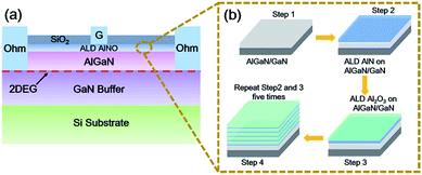 |
| | Fig. 1 (a) Schematic cross sectional view of AlGaN/GaN MIS diode with AlNO nano-films as the gate dielectrics. (b) The process flow charts of AlNO nano-films on AlGaN/GaN heterojunction. | |
Fig. 1(b) shows the process flow charts of AlNO nano-films on AlGaN/GaN heterojunction. In total, 5 periods of AlNO nano-films were deposited and each period contained 7 cycles of AlN followed by 14 cycles of Al2O3. The thicknesses of one PEALD cycle of AlN and Al2O3 were 0.09 nm and 0.12 nm, respectively, confirmed by the spectroscopic ellipsometer (SE). As reference, 90 cycles of Al2O3 was also deposited on AlGaN/GaN heterojunction. Post deposition annealing (PDA) process was performed in nitrogen at 600 °C for 30 s to promote interdiffusing of AlN and Al2O3. Then, electron beam evaporation (EBE) was performed to deposit the gate-electrode Ni (30 nm)/Au (100 nm) on AlNO or Al2O3. Post metallization annealing (PMA) was implemented in a 95% N2 and 5% H2 mixed atmosphere at 400 °C for 3 minutes to improve the interface between the dielectric layers and Ni/Au. Finally, 200 nm SiO2 was deposited by plasma enhanced chemical vapor deposition (PECVD) as the insulator between electrodes.
X-ray photoelectron spectroscopy (XPS) was performed with Al Kα X-ray from Axis Ultra DLD equipment to analyze the elemental compositions of AlNO nano-films on AlGaN/GaN heterojunction, and the binding energy (BE) was calibrated to the position of the C 1s peak at 284.8 eV. The spectra were curve-fitted with a combination of Gaussian and Lorentzian line shapes using a Shirley-type background subtraction. For the investigation of dielectrics/AlGaN interface, a period of AlNO nano-films and 18 PEALD cycles of Al2O3 nano-films were deposited on the AlGaN/GaN heterojunction, respectively. High resolution transmission electron microscopy (HRTEM) was carried out to show the cross-section microstructure of the dielectric/AlGaN interface. The leakage current (J–V) and capacitance–voltage (C–V) measurements were carried out to reveal the high quality of AlNO nano-films on AlGaN/GaN heterojunction. In addition, the frequency- and voltage-dependent conductance method was utilized to characterize the interface trap density at the dielectric/AlGaN interface.
3. Results and discussion
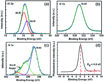
The XPS Al 2p, O 1s, N 1s and O 1s loss energy spectra of AlNO nano-films on AlGaN/GaN heterojunction were illustrated in Fig. 2. The peaks of Al 2p spectra, as shown in Fig. 2(a) could be fitted by two sub-peaks located at 74.1 eV and 74.8 eV, which were corresponding to Al–N and Al–O bonds, respectively.28,29 Fig. 2(b) showed the symmetric O 1s peak located at 530.9 eV corresponding to the O–Al bonds, indicating nitrogen was not oxidized during the PEALD and the subsequent annealing processes. As shown in Fig. 2(c), the N 1s peak could be fitted by three sub-peaks located at 394.1, 395.5 and 397.1 eV, respectively. The sub-peak located at 397.1 eV was assigned to the N–Al bonds,22 whereas the peaks located at 394.1 and 395.5 eV were identified as the Ga–N Auger peaks, which were originated from the AlGaN substrate.30,31 It was worth to mention that no N–O bonds was detected, further confirming the nitrogen was not oxidized. Furthermore, XPS quantitative analysis was employed to determine the chemical composition of the AlNO nano-films. The atomic fractions in AlNO nano-films was Al (41.5%)–N (5.2%)–O (53.3%). O 1s energy-loss spectrum was also performed to calculate the band gap of AlNO nano-films on AlGaN/GaN heterojunction, as is shown in Fig. 2(d). The obtained band gap of AlNO was 6.8 eV, which was between the band gap of pure Al2O3 (7.3 eV) and AlN (6.4 eV) reported in the literature.32,33
 |
| | Fig. 2 XPS spectra of (a) Al 2p, (b) O 1s, (c) N 1s, and (d) O 1s energy-loss spectra of AlNO nano-films on AlGaN/GaN heterojunction. | |
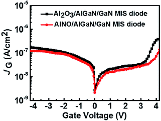
Fig. 3 showed the leakage current density (JG) versus gate voltage (VG) for the AlNO/AlGaN/GaN and Al2O3/AlGaN/GaN MIS diodes. Compared to the AlGaN/GaN MIS diode with Al2O3 nano-films, the AlNO nano-films exhibited a well-suppressed gate leakage current density of 3.45 × 10⁻⁸ A cm−2 up to a forward bias of 3.5 V and the corresponding the breakdown electrical field was up to 3.2 MV cm−1. Specially, the reported breakdown electrical field of AlNO deposited by N2 plasma incorporation in ALD Al2O3 was only 1.5 MV cm−1.22 These data implied that oxygen diffusion could be effectively suppressed by alternant AlN incorporation in Al2O3, resulting in a lower leakage current density and a higher breakdown electrical field of AlNO/AlGaN/GaN MIS diode than that for Al2O3/AlGaN/GaN MIS diode.
 |
| | Fig. 3 JG–VG characteristics of AlNO/AlGaN/GaN and Al2O3/AlGaN/GaN MIS diodes. | |
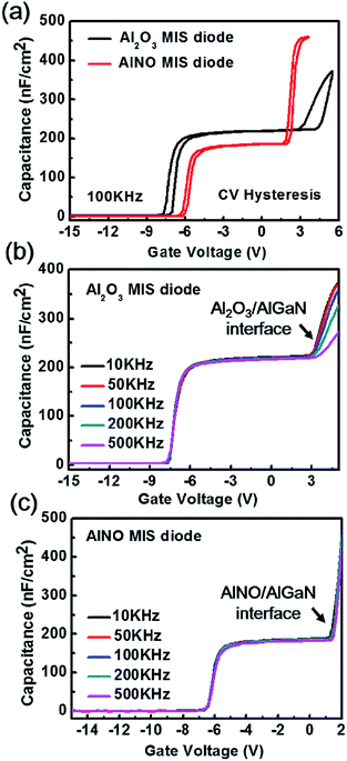
Fig. 4 showed the hysteresis and multi-frequency C–V curves of Al2O3/AlGaN/GaN and AlNO/AlGaN/GaN MIS diodes. There existed two abrupt slops in all C–V curves, one was at negative voltage corresponding to the accumulation at 2DEG interface, and the other one was at positive voltage corresponding to the gate dielectric/AlGaN interface. The dielectric constant of the AlNO nano-films deduced from the C–V curves was 6.9, which was slightly less than that of Al2O3 (7.4). Due to the smaller dielectric constant of AlNO, it had a smaller capacitance than Al2O3 under the same thickness and area. In addition, dielectrics were in series to AlGaN on GaN. Therefore, a smaller voltage would be sustained by the AlNO with respect to the Al2O3 when the same voltage was applied at the gate, leading to a smaller bend up voltage in the second abrupt slop of the C–V curves in the AlNO/AlGaN/GaN MIS diode. The hysteresis C–V curves, measured at 100 kHz from all samples were shown in Fig. 4(a). Compared to the Al2O3/AlGaN/GaN MIS diode, the diode with AlNO nano-films achieved a positive Vfb shift of 1.50 V and a negligible Vfb hysteresis, which indicated that AlN incorporating into Al2O3 would compensate the positive fixed charge within Al2O3.34,35 The second step reflected the state of gate-dielectrics/AlGaN interface, and compared to the Al2O3/AlGaN/GaN MIS diode, the AlNO/AlGaN/GaN MIS diode exhibited a significant reduced hysteresis, indicating there was an excellent interface quality at the AlNO/AlGaN interface. In addition, the dynamic capacitance dispersion measurement was also accomplished to further analyze the dielectric/AlGaN interface. The measured C–V curves with frequency varied from 10 kHz to 500 kHz were shown in Fig. 4(b) and (c). The frequency dispersion of capacitance in C–V curves due to the dielectric/AlGaN interface trap response was observable in the second slope region for both samples. For one given f, only those interface traps with energy level (ET) aligned to Fermi level (EF) and τit shorter than 1/f could respond to ac anode signal and contribute additional capacitance with VG increasing. With a higher frequency f, larger VG was required to raise the EF towards conduction band (EC) so that the shallower interface traps with smaller τit could respond, resulting in frequency dispersion of capacitance in the second slope bias region.18 Severe frequency dispersion of capacitance in the Al2O3/AlGaN/GaN MIS diode was attributed to high-density interface trap because of the presence of detrimental interfacial layer Ga-suboxide (GaOx) shown in Fig. 4(b). As shown in Fig. 4(c), the frequency dispersion was effectively suppressed in the AlNO/AlGaN/GaN MIS diode, indicating the interface trap density was significantly reduced. As a result, insertion of AlN in Al2O3 could potently suppress the formation of unstable interfacial layers such as GaOx at the AlNO/AlGaN interface.
 |
| | Fig. 4 (a) Hysteresis C–V curves of AlNO/AlGaN/GaN and Al2O3/AlGaN/GaN MIS diodes; (b) multi-frequency C–V curves of Al2O3/AlGaN/GaN MIS diode; (c) multi-frequency C–V curves of AlNO/AlGaN/GaN MIS diode. | |
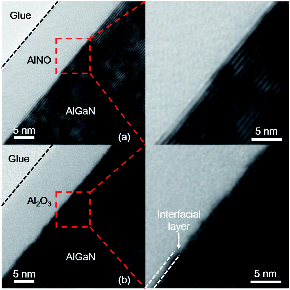
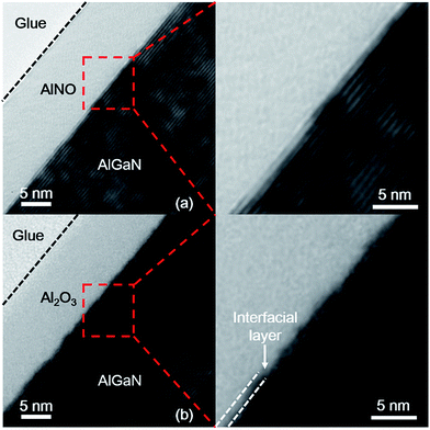
The cross-section microstructures of AlNO/AlGaN and Al2O3/AlGaN interface were both investigated by HRTEM, as shown in Fig. 5(a) and (b), respectively. There was a rough and nearly ∼2 nm interfacial layer at the Al2O3/AlGaN interface, which was originated from the GaOx formed during the Al2O3 deposition. Nevertheless, in the AlNO/AlGaN/GaN MIS diode, the AlN layer not only could act as a passivation layer on AlGaN, but also could serve as a separation membrane to suppress the oxidation process during subsequent Al2O3 deposition. By alternative deposition of AlN and Al2O3 layer to form AlNO nano-films on AlGaN/GaN heterojunction, a uniform and sharp AlNO/AlGaN interface could be obtained. It was worth to mention that intermixed Al2O3 and AlN rather than Al2O3 and AlN overlays was obtained in our work. This conjecture was firstly supported by the fact that no layered structures were observed by HRTEM (Fig. 5(a)). Furthermore, it could also be confirmed by the huge difference in per-unit-length capacitance between AlNO nano-films and segregated Al2O3/AlN layers. The per-unit-length capacitances of pure Al2O3 and AlN on AlGaN/GaN were 573 nF cm−2 and 1270 nF cm−2, respectively,33 and the calculated per-unit-length capacitance of segregated Al2O3 (8 nm)/AlN (3 nm) layers was 126 nF cm−2, which was much less than the measured capacitance of AlNO nano-films (580 nF cm−2). The high per-unit-length capacitance of AlNO nano-films was due to incorporation of AlN into Al2O3 and this result agreed well with the reports of M. Cho et al. and C. An et al.36,37 We thus proposed that the AlNO nano-films fabricated using the approach described in this paper was effectively Al2O3–AlN alloy. In addition, the PDA process at 600 °C could indeed promote interdiffusion of AlN and Al2O3, but the aim of performing 600 °C PDA was to prove that AlNO nano-films could maintain the amorphous state even at 600 °C annealing due to Al2O3 incorporation. AlN was known to crystallize even at 500 °C and lead to a serious gate leakage current.33
 |
| | Fig. 5 High resolution transmission electron microscopy (HRTEM) micrographs of (a) Al2O3/AlGaN and (b) AlNO/AlGaN interfaces. | |
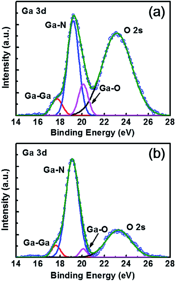
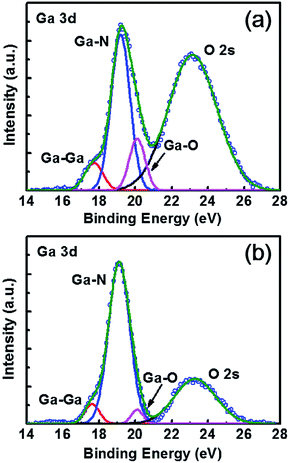
To investigate the difference of interface chemistry and bonding states between AlNO/AlGaN and Al2O3/AlGaN interfaces, the evolution of Ga 3d core-level spectra of AlNO/AlGaN and Al2O3/AlGaN interfaces were both demonstrated. As shown in Fig. 6(a), the Ga–O peak of Al2O3/AlGaN interface was obvious while a lower intensity of Ga–O peak at the AlNO/AlGaN interface was obtained (shown in Fig. 6(b)), manifesting that the GaOx were effectively suppressed by the alternative growth of AlN and Al2O3 in AlNO nano-films.
 |
| | Fig. 6 XPS spectra of Ga 3d core levels of (a) 18 cycles growth of Al2O3 films on AlGaN/GaN heterojunction, and (b) one period cycles growth of AlNO nano-films on AlGaN/GaN heterojunction. | |
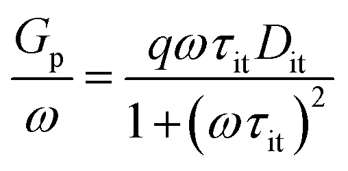
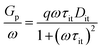
The frequency- and voltage-dependent conductance measurement was carried out to quantitative deduce the interface trap distribution.38 With the MIS diode biased at the second slope in the C–V curves, AlGaN/GaN heterojunction interface trap located in the band gap were far below the Fermi level, thus only the dielectric/AlGaN interface trap could respond to the ac signal. The measurement frequency was ranging from 1 kHz to 1 MHz at room temperature. The equivalent parallel conductance Gp/ω was given by the following equation,
| |
 | (3) |
where
ω = 2π
f was the radial frequency,
τit was trap time constant, and
Dit was the interface trap density. The parallel conductance
Gp/
ω was related to the measured capacitance
Cm and conductance
Gm, and could be calculated from the relation:
| |
 | (4) |
where
Cb represented the static-state capacitance of MIS diodes, and the measured capacitance
Cm represented the series connection of the trap capacitance
Ctrap to the dielectric layer capacitance
Cdielectrics and the AlGaN layer capacitance
CAlGaN.
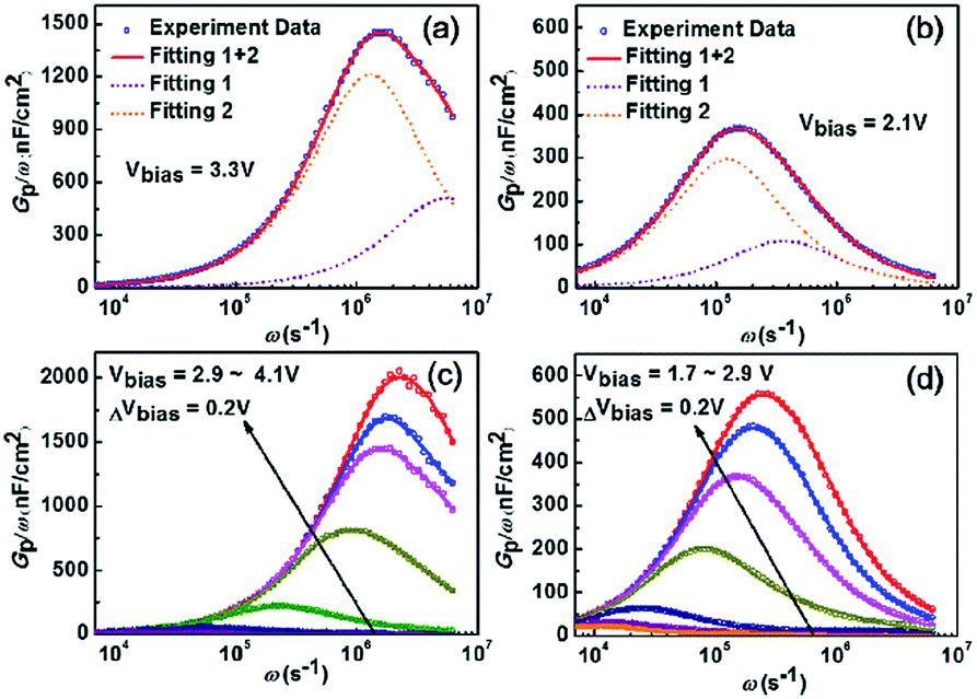
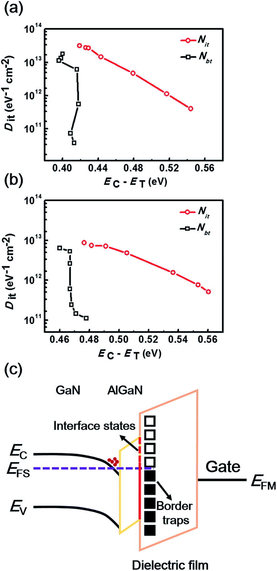
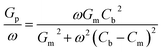
The Dit and the corresponding τit at the dielectric/AlGaN interface could be extracted by fitting the experimental data using eqn (3). As shown in Fig. 7(a) and (b), both the Gp/ω curves for AlNO/AlGaN/GaN and Al2O3/AlGaN/GaN MIS diodes could be resolved into the superposition of two fitting curves at the given bias voltage of 3.3 V and 2.1 V, respectively, indicating there were two types of trap states presenting at the dielectrics/AlGaN interface, i.e., interface states and border traps. Border traps were the near interfacial oxide traps and could be regarded as either interface traps or bulk oxide traps, relating to the gate bias, voltage ramp rate and measurement frequency. The densities of both interface states (Nit) and border traps (Nbt) were determined to characterize the interface properties. As exhibited in Fig. 7(c) and (d), similar fitting results could be obtained in the voltage bias range of 2.9 V to 4.1 V and 1.7 V to 2.9 V for both AlNO/AlGaN/GaN and Al2O3/AlGaN/GaN MIS diodes, respectively. For clarity, only superposed fitting curves were presented.
 |
| | Fig. 7 The measured curves and fitting curves of Gp/ω vs. ω at the Vbias of 3.3 V and 2.1 V for (a) Al2O3/AlGaN/GaN and (b) AlNO/AlGaN/GaN MIS diodes, respectively. Measured curves and fitting curves of Gp/ω vs. ω at the Vbias of 2.9 to 4.1 V and 1.7 to 2.9 V for (c) Al2O3/AlGaN/GaN and (d) AlNO/AlGaN/GaN MIS diodes, respectively. Each fitting curve was the superposition of fitting 1 and fitting 2 for both diodes. | |
The energy levels ET of traps with respect to EC, i.e. EC − ET, were related to it through the following equation,39
| |
 | (5) |
where
T was room temperature (300 K),
σn = 4 × 10
−13 cm
2 was the electron capture cross section,
Nc = 2.2 × 10
18 cm
−3 represented the effective density of states in Al
0.25Ga
0.75N conduction band, and
νth = 2.6 × 10
7 cm s
−1 was the thermal velocity.
40 The dependence of
Dit on trap energy level
EC −
ET could be extracted by using
eqn (3) and
(5) and shown in
Fig. 8. The interface states exhibited strong continuous distribution in energy level, and the energy level of border traps were located at a very narrow energy range. Compared to the Al
2O
3/AlGaN/GaN MIS diode with a
Nit of 10
13 to 10
11 eV
−1 cm
−2 in the energy level range of 0.42 eV to 0.54 eV (
Fig. 8(a)), the
Nit in the AlNO/AlGaN/GaN MIS diode varied from 10
12 to 10
11 eV
−1 cm
−2 with the energy level range of 0.48 eV to 0.56 eV (
Fig. 8(b)), indicating the interface states density was significantly reduced and the GaO
x was effectively suppressed at the AlNO/AlGaN interface. In addition, the introduced AlN layer could also separate oxide border traps near the interface in the AlNO nano-films. As a result, both high quality border region and reduced
Nbt could be obtained. The schematic band diagram of interface states and border traps was shown in
Fig. 8(c). For a positive gate bias voltage, the conduction band of the AlGaN barrier could be pulled down and the electrons would transfer from the channel to the dielectrics/AlGaN interface, where they were trapped or detrapped by interface states or border traps.
 |
| | Fig. 8 Dependence of interface trap density on trap energy level below AlGaN conduction band at (a) Al2O3/AlGaN and (b) AlNO/AlGaN interfaces. (c) Schematic band diagram of interface states and border traps in the dielectric/AlGaN/GaN MIS diodes. | |
4. Conclusions
In conclusion, by alternating growth of AlN and Al2O3 nano-lamination using NH3 and O2 plasma in a PEALD process, AlGaN/GaN MIS diode with AlNO nano-films as the gate dielectric has been fabricated. With the insertion of AlN layer, the AlNO/AlGaN features a sharp interface with effective suppression of AlGaN surface oxidation, leading to significantly reduced hysteresis and frequency-dispersion of C–V characteristics. In addition, nitrogen incorporation can produce negative fixed charge in Al2O3 gate dielectric, which was contributed to positive shift in the flat band voltage. Compared with the Al2O3/AlGaN/GaN MIS diode, an improved interface with a lower interface states and reduced border traps was obtained in the AlNO/AlGaN/GaN MIS diode. The manufacture of AlNO nano-films by PEALD could provide a pathway to achieve the operation of enhancement mode AlGaN/GaN MIS-HEMTs with low interface trap density.
Acknowledgements
This work is funded by the National Natural Science Foundation of China (Grant No. 16ZR1442300) and the Natural Science Foundation of Shanghai (Grant No. Y52GXA1J01).
Notes and references
- H. Nie, Q. Diduck, B. Alvarez, A. P. Edwards, B. M. Kayes, M. Zhang, G. F. Ye, T. Prunty, D. Bour and I. C. Kizilyalli, IEEE Electron Device Lett., 2014, 35, 939 CrossRef CAS.
- D. W. Seo, H. G. Choi, J. Twynam, K. M. Kim, J. S. Yim, S. W. Moon, S. Jung, J. Lee and S. D. Roh, IEEE Electron Device Lett., 2014, 35, 446 CrossRef CAS.
- C. Y. Tsai, T. L. Wu and A. Chin, IEEE Electron Device Lett., 2012, 33, 35 CrossRef CAS.
- M. J. Wang and K. J. Chen, IEEE Trans. Electron Devices, 2011, 58, 460 CrossRef CAS.
- R. Vetury, N. Q. Zhang, S. Keller and U. K. Mishra, IEEE Trans. Electron Devices, 2001, 48, 560 CrossRef CAS.
- J. Joh, A. Del, A. Jesús and J. Jimenez, IEEE Electron Device Lett., 2008, 25, 665 CrossRef.
- U. K. Mishra, P. Y. Parikh and F. Wu, Proc. IEEE, 2002, 90, 1022 CrossRef CAS.
- P. D. Ye, B. Yang, K. K. Ng, J. Bude, G. D. Wilk, S. Halder and J. C. M. Hwang, Appl. Phys. Lett., 2005, 86, 603501 Search PubMed.
- Y. Hao, L. Yang, X. H. Ma, J. G. Ma, M. Y. Cao, C. Y. Pan, C. Wang and J. C. Zhang, IEEE Electron Device Lett., 2011, 32, 626 CrossRef CAS.
- C. Liu, E. F. Chor and L. S. Tan, Appl. Phys. Lett., 2006, 88, 173504 CrossRef.
- G. Ye, H. Wang, S. Arulkumaran, G. I. Ng, R. Hofstetter, Y. Li, M. J. Anand, K. S. Ang, Y. K. T. Maung and S. C. Foo, Appl. Phys. Lett., 2013, 103, 142109 CrossRef.
- D. A. Deen, D. F. Storm, R. Bass, D. J. Meyer, D. S. Katzer, S. C. Binari, J. W. Lacis and T. Gougousi, Appl. Phys. Lett., 2011, 98, 023506 CrossRef.
- S. Huang, S. Yang, J. Roberts and K. J. Chen, Jpn. J. Appl. Phys., 2011, 50, 110202 CrossRef.
- J. Robertson, Eur. Phys. J.: Appl. Phys., 2004, 28, 265 CrossRef CAS.
- R. D. Long and P. C. McIntyre, Materials, 2012, 5, 1297 CrossRef CAS.
- S. Yang, Z. Tang, K. Y. Wong, Y. S. Lin, C. Liu, Y. Lu, S. Huang and K. J. Chen, IEEE Electron Device Lett., 2013, 34, 1497 CrossRef CAS.
- X. Y. Qin, H. Dong, B. Brennan, A. Azacatl, J. Y. Kim and R. M. Wallace, Appl. Phys. Lett., 2013, 103, 221604 CrossRef.
- S. H. Liu, S. Yang, Z. K. Tang, Q. M. Jiang, C. Liu, M. J. Wang, B. Shen and K. J. Chen, Appl. Phys. Lett., 2015, 106, 051605 CrossRef.
- P. Lagger, A. Schiffmann, G. Pobegen, D. Pogany and C. Ostermaier, IEEE Electron Device Lett., 2013, 34, 1112 CrossRef CAS.
- C. L. Hinkle, M. Milojevic, B. Brennan, A. M. Sonnet, F. S. A. Tostado, G. J. Hughes, E. M. Vogel and R. M. Wallace, Appl. Phys. Lett., 2009, 94, 162101 CrossRef.
- J. J. Zhu, X. H. Ma, Y. Xie, B. Hou, W. W. Chen, J. C. Zhang and Y. Hao, IEEE Trans. Electron Devices, 2015, 62, 512 CrossRef CAS.
- M. A. Negara, M. Kitano, R. D. Long and P. C. McIntyre, ACS Appl. Mater. Interfaces, 2016, 8, 21089 CAS.
- L. Zheng, X. H. Cheng, Y. H. Yu, Y. H. Xie, X. L. Li and Z. J. Wang, Phys. Chem. Chem. Phys., 2015, 17, 3179 RSC.
- R. Suri, C. J. Kirkpatrick, D. J. Lichtenwalner and V. Misra, Appl. Phys. Lett., 2010, 96, 042903 CrossRef.
- L. Zheng, X. H. Cheng, P. Y. Ye, L. Y. Shen, Q. Wang, D. L. Zhang, Z. J. Wang, Y. H. Yu and X. K. Yu, J. Mater. Chem. C, 2016, 4, 11067 RSC.
- S. Heo, D. l. Tahir, J. G. Chung, J. C. Lee, K. H. Kim, J. Lee, H. Lee, G. S. Park, S. K. Oh, H. J. Kang, P. Choi and B. D. Choi, Appl. Phys. Lett., 2015, 107, 182201 CrossRef.
- M. Choi, J. L. Lyons, A. Janotti and C. G. Van de Walle, Appl. Phys. Lett., 2013, 102, 142902 CrossRef.
- A. Mahmood, R. Machorro, S. Muhl, J. Heiras, F. F. Castillon, M. H. Farias and E. Andrade, Diamond Relat. Mater., 2003, 12, 1315 CrossRef CAS.
- M. Zhu, P. Chen, R. K. Y. Fu, W. Liu, C. Lin and P. K. Chu, Appl. Surf. Sci., 2005, 239, 327 CrossRef CAS.
- C. Ozgit-Akgun, E. Goldenberg, A. K. Okyay and N. J. Biyikli, J. Mater. Chem. C, 2014, 2, 2123 RSC.
- G. Moldovan, I. Harrison, M. Roe and P. D. Brown, Inst. Phys. Conf. Ser., 2004, 179, 115 CAS.
- L. Zheng, X. H. Cheng, D. Cao, G. Wang, Z. J. Wang, D. W. Xu, C. Xia, L. Y. Shen, Y. H. Yu and D. Shen, ACS Appl. Mater. Interfaces, 2014, 6, 7014 CAS.
- D. Cao, X. H. Cheng, Y. H. Xie, L. Zheng, Z. J. Wang, X. K. Yu, J. Wang, D. W. Xu, Y. H. Yu and D. S. Shen, RSC Adv., 2015, 5, 37881 RSC.
- J. Son, V. Chobpattana, B. M. McSkimming and S. Stemmer, Appl. Phys. Lett., 2012, 101, 102905 CrossRef.
- T. H. Hung, S. Krishnamoorthy, M. Esposto, D. N. Nath, P. S. Park and S. Rajan, Appl. Phys. Lett., 2013, 102, 072105 CrossRef.
- M. Cho, H. S. Chang, Y. J. Cho, D. W. Moon, K. Min, R. Sinclair, S. K. Kang, D. Ko, J. H. Lee, J. H. Gu and N. I. Lee, Appl. Phys. Lett., 2004, 84, 571 CrossRef CAS.
- C. An, C. Mahata, Y. Byun and H. Kim, J. Phys. D: Appl. Phys., 2013, 46, 275301 CrossRef.
- X. H. Ma, J. J. Zhu, X. Y. Liao, T. Yue, W. W. Chen and Y. Hao, Appl. Phys. Lett., 2013, 103, 033510 CrossRef.
- M. Silvestri, M. J. Uren and M. Kuball, Appl. Phys. Lett., 2013, 102, 073501 CrossRef.
- P. Kordos, R. Stoklas, D. Gregusoa and J. Novak, Appl. Phys. Lett., 2009, 94, 223512 CrossRef.
|
| This journal is © The Royal Society of Chemistry 2017 |
Click here to see how this site uses Cookies. View our privacy policy here. 
 Open Access Article
 This Open Access Article is licensed under a
  *ab,
Xinhong Cheng*a,
Li Zhengab,
Lingyan Shenab,
Jingjie Liab,
Dongliang Zhangab,
Ru Qianab and
Yuehui Yua
*ab,
Xinhong Cheng*a,
Li Zhengab,
Lingyan Shenab,
Jingjie Liab,
Dongliang Zhangab,
Ru Qianab and
Yuehui Yua