
 Open Access Article
 This Open Access Article is licensed under a Creative Commons Attribution-Non Commercial 3.0 Unported Licence
Metal acetate based synthesis of small-sized Cu2ZnSnS4 nanocrystals: effect of injection temperature and synthesis time†
A. Irkhina *a,
S. Levcenkoa,
V. Hinrichsb,
P. Plateb and
T. Unold*a
*a,
S. Levcenkoa,
V. Hinrichsb,
P. Plateb and
T. Unold*a
aDepartment Structure and Dynamics of Energy Materials, Helmholtz-Zentrum Berlin für Materialien und Energie GmbH, Berlin 14109, Germany. E-mail: unold@helmholtz-berlin.de; anastasia.irkhina@helmholtz-berlin.de
bInstitute for Solar Fuels, Helmholtz-Zentrum Berlin für Materialien und Energie, Berlin 14109, Germany
First published on 16th February 2017
Abstract
We report the colloidal synthesis of small-sized Cu2ZnSnS4 (CZTS) nanocrystals (NCs) via a hot-injection method using zinc and tin acetates in combination with copper acetylacetonate as metal precursors. A systematic investigation of the influence of the injection temperature in the range from 190 °C to 300 °C on the size distribution, composition and phase purity of CZTS nanocrystals has been performed. It has been found that temperature plays the key role in changing of the metal sources reactivity and influences the final composition of the nanocrystals. The mechanism of nanocrystal formation has been investigated by Raman spectroscopy of aliquots of their solutions. It starts from the formation of a Cu2−xS phase as a core followed by the incorporation of Zn2+ and Sn4+ atoms into its structure regardless of injection temperature.
Introduction
Over the last decade photovoltaic thin film devices based on solution-processed absorber layers, which includes nanocrystal ink-based film deposition, have become highly competitive in comparison to vacuum methods, in particular for kesterite-based solar cells.1,2 Non-vacuum approaches for the synthesis of kesterite materials have the advantages of providing relatively homogeneous films, simplicity of preparation and low material usage. The kesterite-type Cu2ZnSnS4 semiconductor consists of non-toxic and earth abundant elements. This factor in combination with an energy band gap value well-matched the solar spectrum and a high absorption coefficient, more than 104 cm−1 above the band edge, makes CZTS an ideal candidate for photovoltaic applications.Colloidal synthesis routes allow tuning of the composition, phase and size distribution for the wide range of elemental and binaries nanocrystals.3–6 The application of this method to ternary and quaternary systems such as CuInS(Se)2, CuInxGa1−xS2 and CZTSSe gives the opportunity to obtain NCs with a specifically tuned energy band gap and optoelectronic properties.7–9
Due to the various degrees of freedom of the quaternary CZTS compound, secondary phases are easily formed and composition control is an important aspect in the synthesis of this material.10,11 The nature of precursors and growth temperature value play an important role for the nucleation and growing processes.
CZTS nanocrystals with narrow size distribution have been obtained by hot-injection synthesis, by the ‘heat up’ approach or by thermal decomposition of single-source precursors such as metal dithiocarbamate complexes.12–14 Despite the fact that the tetragonal kesterite phase is the most thermodynamically stable phase for the CZTS compound, nanocrystals with metastable wurtzite structure have been also synthesized utilizing thiols as sulfur source which has a strong coordination between thiol group and metal cations (Cu+, Zn2+).15,16 It has been noted that for the formation of the kesterite phase it is necessary to use low reactivity precursors, solvents and surfactants with weak coordination toward metal cations such as oleylamine (OAm).17
In terms of the nucleation rate of the nanocrystals it is very important to control the reactivity of the elemental sources. For instance, using such chemicals as thiourea (TU) or thioacetamide (TAA) leads to a lower rate of H2S release in comparison to an elemental sulfur source.18 On the other hand, differences in and a deliberate tuning of the reactivity of the metal precursors should considered.
The hot injection method has several advantages over other wet chemical methods such as the potential high quality of the obtained nanocrystals, narrow size distributions and the control of the mean particle size. Although there are many reports of CZTS nanocrystals synthesized by the hot-injection method, the influence of the injection temperature on the nanocrystal nucleation and growth has not been extensively investigated so far.19 Besides that, it is still unclear which size of the NCs is better suited for solar cells fabrication. Previously reported recipes based on this technique usually result in nanocrystals with an average size of 7–20 nm.1,18,20,21 In this paper we report a recipe for the synthesis of small-sized CZTS nanocrystals (∼4–5 nm), where zinc acetate, tin acetate and copper acetylacetonate as metal precursors in combination with OAm have been used. The effect of the injection temperature on the morphology, chemical composition and secondary phase formation has been systematically investigated. Based on the detailed Raman scattering analysis of the aliquots taken at different growth time, the formation mechanism of CZTS nanocrystals has been proposed.
Experimental section
Materials
Copper(II) acetylacetonate (Cu(acac)2; ≥99.99% trace metal basis), zinc(II) acetate (Zn(CH3COO)2; ≥99.99% trace metal basis), tin(IV) acetate (Sn(CH3COO)4; ≥99.99% trace metal basis), elemental sulfur (powder, 99.98% trace metals basis), oleylamine (OAm; technical grade, 70%), hexane (≥99%), acetone (≥99.5%) and methanol (≥99.8%) were purchased from Sigma Aldrich. All reagents were used as received without further purification.Synthesis of CZTS nanocrystals
Due to the fact that the best efficiencies of CZTS solar cells have been consistently obtained for Cu-poor and Zn-rich absorber layers,22 the initial ratio of precursors in the present work were taken as Cu/Sn = 1.76 and Zn/Sn = 1.05 (Cu/(Zn + Sn) = 0.86). Quaternary nanocrystals were synthesized using the hot-injection method. For the preparation of metal precursor Cu(acac)2 (1.32 mmol, 0.3455 g), Zn(CH3COO)2 (0.79 mmol, 0.1449 g), Sn(CH3COO)4 (0.75 mmol, 0.2662 g) were dissolved in 10 ml of oleylamine in three-neck flask and connected via a water-cooled condenser to a Schlenk line. The reaction mixture was permanently stirred under vacuum for 10 min at room temperature and then for 30 min at 120 °C. Then the mixture was placed under a nitrogen atmosphere and heated to 140 °C for 40 min including heating up followed by further heating to the injection temperature.Separately the sulfur precursor solution (1 M) was prepared by dissolving of elemental sulfur in oleylamine in a 25 ml two-neck flask. The solution was placed under vacuum at 60 °C in an ultrasonic bath for 1 hour. The flask was connected to the nitrogen line with permanent heating until total dissolution of the sulfur powder.
4 ml of sulfur solution at 60 °C was injected to the metal precursor solution via a rubber septum at varied temperatures. After the injection the reaction mixture immediately changed the color to dark-brown. Injection temperatures between 190 °C and 300 °C were used. The system was kept at the injection temperature for 40 min and then cooled down and disconnected from the heating source. The experimental details are summarized in Table S1 (ESI†).
Cleaning of nanocrystals
The main goal of the cleaning step is to minimize the amount of oleylamine in the nanoparticle ink since it has a strong influence on the structural and optical characterization. Appropriate solvents for cleaning should dissolve oleylamine, be partially immiscible with hexane, which is used as nanocrystals solvent, and be polar. For this purpose acetone and methanol have been chosen. The NCs–oleylamine solution was centrifuged using an acetone/methanol mixture (ratio 3![[thin space (1/6-em)]](https://www.rsc.org/images/entities/char_2009.gif) :1) for 10 min at 9000 rpm after which all the particles had settled down at the bottom of the tube. At the same time the resulting supernatant was semi-transparent and red-orange in color (sulfur/oleylamine solution). The settled nanocrystals were redissolved in hexane (1 ml), diluted with acetone/methanol mixture (ratio 2:3) and centrifuged. This procedure was repeated several times. After the total cleaning procedure the nanocrystals were dispersed in 6 ml of hexane. For the Raman characterization additional cleaning of nanocrystals from organic residual has been performed as it was found that an excess of organic ligands in the sample can significantly reduce the signal-to-noise ratio.
:1) for 10 min at 9000 rpm after which all the particles had settled down at the bottom of the tube. At the same time the resulting supernatant was semi-transparent and red-orange in color (sulfur/oleylamine solution). The settled nanocrystals were redissolved in hexane (1 ml), diluted with acetone/methanol mixture (ratio 2:3) and centrifuged. This procedure was repeated several times. After the total cleaning procedure the nanocrystals were dispersed in 6 ml of hexane. For the Raman characterization additional cleaning of nanocrystals from organic residual has been performed as it was found that an excess of organic ligands in the sample can significantly reduce the signal-to-noise ratio.
Characterization
For the characterization of the nanocrystal shape and size, transmission electron microscopy (TEM) was performed using a Philips CM12 with an accelerating voltage of 120 kV. The samples were prepared by drop-casting of low concentrated nanocrystal ink onto a carbon-coated meshed grid. Structural characterization of colloidal nanocrystals was investigated by Grazing Incidence X-Ray Diffraction (GIXRD) using a PANalytical X'pert Pro MPD diffractometer operating with Cu Kα-radiation (λ = 1.54056 Å). Laser ablation-inductively coupled plasma-mass spectrometry (LA-ICP-MS) has been used for measuring the chemical composition of samples prepared by drop casting a concentrated dispersion of nanocrystals in hexane on a Mo-coated soda lime glass substrate. Measurements were performed in multiline scans using a LSX213 laser system by CETAD and for the laser ablation part and the ICP-MS 4500 (Hewlett Packard) to ionize the ablated material in an argon plasma and detect the ions with a quadrupole mass spectrometer. High laser power was chosen to reduce the effects of elemental fractionation. Pressed kesterite powders, characterized by micro probe were used as a reference sample. Raman scattering measurements were performed using a confocal micro Raman system (Horiba LabRam HR Evolution) with a He–Ne red excitation laser of 632.8 nm, with an average power on sample surface less than 1 mW. For UV micro – Raman measurements the 325 nm He–Cd laser line was used for excitation in the backscattering geometry. The scattered light was collected using a triple monochromator system equipped with a charge-coupled device camera. To calibrate detection system a reference silicon wafer with 520.7 cm−1 peak position was used. UV-Vis-NIR absorption spectra of CZTS nanoparticle solution were measured in hexane on a Perkin Elmer Lambda 950 UV/Vis/NIR spectrophotometer with 1 cm path length quartz cuvettes.Results and discussion
We have synthesized CZTS nanocrystals by the hot-injection method using different injection temperatures in the range of 190–300 °C. The morphology and size distribution of the obtained nanocrystals are shown in Fig. 1. It can be seen that the reported synthesis method leads to the preferential formation of small-sized NCs and that the injection temperature has a strong influence on the size distribution. An injection of the sulfur precursor at 200 °C leads to the formation of nanocrystals with an average size 5.1 ± 0.9 nm (Fig. 1a and f). An increase of the temperature to 225 °C and then to 250 °C leads to narrowing of the size distribution and to a decrease of the average size to 3.9 ± 0.6 nm (Fig. 1b and g) and 4.6 ± 0.7 nm (Fig. 1c and h), respectively. Previously, such small particle sizes have been obtained only using decomposition synthesis methods where diethyl dithiocarbamate complexes of metals decompose thermally to produce their corresponding sulfides.14,23 For the sample obtained at 250 °C small amounts of bigger particles with a size between 10 and 15 nm can be observed (∼5%). Further increasing of the injection temperature to 275 °C and 300 °C leads to a polydispersity of the obtained particles as can be seen in Fig. 1d and e. Evaluating the size distribution shows that samples for both injection temperatures mainly consist of the small sized NP, however with a bimodal distribution including larger size particles. This polydispersity may be a result of the parallel nucleation in the system or due to Ostwald ripening.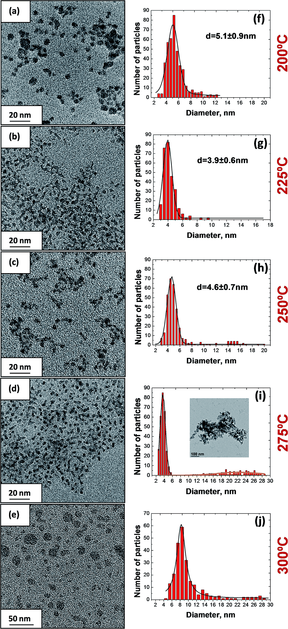 | ||
| Fig. 1 TEM images and size distribution histograms of CZTS nanocrystals obtained at different injection temperatures: 200 °C (a and f), 225 °C (b and g), 250 °C (c and h), 275 °C (d and i) and 300 °C (e and j). | ||
Size control of NPs can be obtained via thermodynamic and/or kinetic means. According to the theory of homogeneous nucleation a decrease of the nanocrystal size can be achieved by a decrease of the critical radius rcr, which represents the most stable particle size for the system due to the lowest Gibbs free energy. This value can be decreased by increasing the supersaturation or by reduction of the surface energy of the nanocrystals, which is influenced by the ligands, solvents and additives in the solution.24 Thus, the reported preferential formation of small particles may have different origins, which will be discussed in the following.
As has been previously reported, an increasing amount of oleylamine reduces the size of the nanocrystals by lowering the surface energy of the particles.23,25,26 However, we found that the reduction of the amount of OAm does not lead to any significant increase of the average nanocrystal size (Fig. S1 in ESI†).
Influence of the precursor reactivity
The second reason of the preferential formation of small sized nanocrystals can be a high reactivity of metal precursors. Metal acetates and metal acetylacetonates are coordination complexes (chelates). The acetate molecule forms a four-membered chelate ring with the metal cation and it is less stable than six-membered metal-acetylacetonate chelate ring.27 Furthermore, the acetate molecule is small with a reduced steric hindrance, which leads to easier releasing of metals. Thus, the presence of metal acetates in the reaction system can decrease the average nanocrystals size due to an increase of the nucleation rate. Additional experiments (synthesis of binaries) show that Cu2−xS nanocrystals synthesized utilizing copper acetylacetonate have an average size ∼15 nm. At the same time the synthesis of zinc and tin sulfides using acetates leads to the formation of small sized nanocrystals (∼4–5 nm) (Fig. S2 in ESI†). Synthesis of copper tin sulfide under the same reaction conditions using copper acetylacetonate and tin acetate leads to small-sized particles (∼7 nm) that prove the effect of acetate to reduce the particle size (Fig. 2).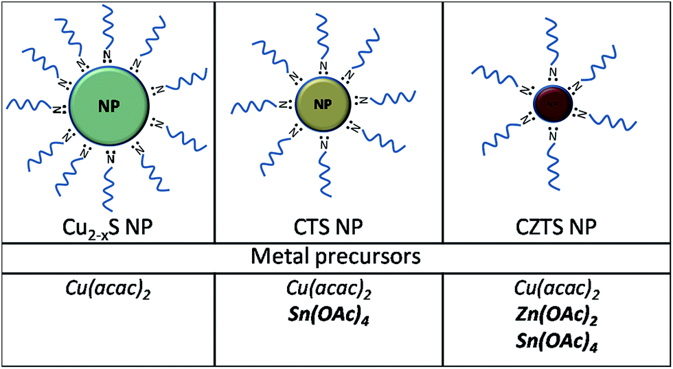 | ||
| Fig. 2 Scheme of the experimentally observed decreasing of the nanocrystal size of Cu2−xS, CTS and CZTS with the increasing amount of acetates in the reaction system. | ||
In order to understand the process of nanocrystal formation the composition of the various synthesized NCs was characterized by LA-ICP-MS (Table 1). For this purpose, two syntheses for each injection temperature have been performed.
| Temperature | Sample series | Cu/Sn | Zn/Sn |
|---|---|---|---|
| 190 °C | a | 1.97 ± 0.25 | 1.10 ± 0.13 |
| 200 °C | a | 2.06 ± 0.26 | 1.13 ± 0.13 |
| b | 2.30 ± 0.27 | 1.29 ± 0.14 | |
| 225 °C | a | 1.60 ± 0.24 | 0.87 ± 0.11 |
| b | 1.7 ± 0.2 | 0.75 ± 0.09 | |
| 250 °C | a | 1.78 ± 0.20 | 1.03 ± 0.12 |
| b | 1.66 ± 0.27 | 0.93 ± 0.14 | |
| 275 °C | a | 1.86 ± 0.24 | 1.04 ± 0.13 |
| b | 1.82 ± 0.25 | 0.88 ± 0.12 | |
| 300 °C | a | 1.87 ± 0.26 | 0.91 ± 0.12 |
| b | 2.13 ± 0.35 | 0.74 ± 0.10 |
Although the as-prepared metal precursor solution was Cu-poor and Zn-rich, the quantitative elemental analysis shows that depending on the injection temperature, the Cu/Sn and Zn/Sn ratios of the nanocrystals deviate from the precursor values (Fig. 3).
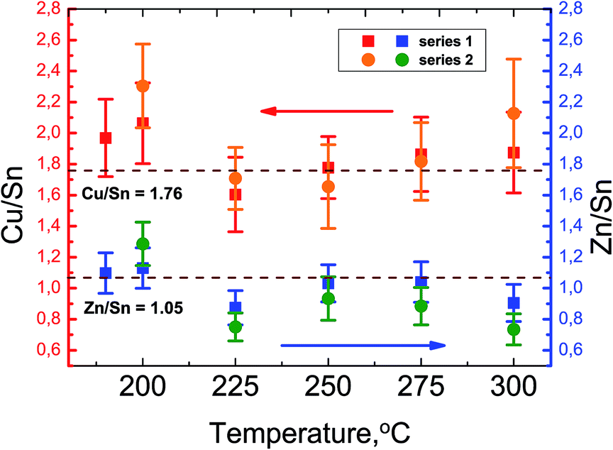 | ||
| Fig. 3 Temperature dependence of the Cu/Sn and Zn/Sn ratios of the obtained nanocrystals according to the LA-ICP-MS analysis (2 series of samples). | ||
We observe that an injection temperature below 200 °C results in a significant Cu- and Zn-richness of the NCs, which means that Sn is poorly incorporated in nanocrystals at low temperature. Further increasing of the injection temperature leads to decreasing of Cu/Sn and Zn/Sn ratios with the lowest value at 225 °C and thereafter increasing slightly again. The weight-in ratios can be achieved in the range of temperatures between 225 °C and 275 °C injection temperature.
The change in cation ratios can be partially explained according to the principle of hard and soft Lewis acids and bases (HSAB).28 Lewis bases donate pairs of electrons and Lewis acids accept pairs of electrons.29 The Cu+ ion behaves as a soft Lewis acid after the Cu(acac)2 decomposition and will have the fastest reactivity with S2− which is a soft Lewis base.30 It has been previously reported that the formation of Cu2−xS phase is the first step of wurtzite and kesterite CZTS nanocrystals formation.31,32 The lowest reactivity can be expected from Sn4+ because of the low affinity of this hard acid for a soft base. Because Zn2+ is a borderline acid, its reactivity to sulfur will be lower than of Cu+, but faster than of Sn4+. At the same time due to basicity of oleylamine, high coordinating power between Sn4+ ion and OAm can lead to Sn-rich nuclei at higher temperatures which influence the Zn/Sn ratio. Thus, in order to achieve Cu-poor composition as desired for CZTS solar cells, the synthesis of nanocrystals by hot injection should utilize reaction temperatures between 225 °C and 275 °C. It can be assumed that at these synthesis temperatures the reactivity difference of metal ions is eliminated and thus it leads to a more homogeneous growth of particles.
In order to investigate the possibility of increasing the Zn content in the NCs additional experiments have been performed with higher weight-in value of Zn/Sn = 1.2 (Fig. S3 in ESI†). However, we found that at Tinj = 225 °C increasing of the zinc content leads to the formation of strongly Cu-rich nanocrystals which is undesirable for solar cells application. At the same time at Tinj = 250 °C there is no significant change in metal composition in comparison with the previous experiments with initial metal ratio Zn/Sn = 1.05. This indicates that the Zn amount which can be incorporated in Cu-poor CZTS nanocrystals is limited.
It was experimentally and theoretically shown that the ternary phase diagram of the Cu2S–ZnS–SnS2 system exhibits a very narrow region of stability for single-phase kesterite.33–35 From a thermodynamic equilibrium point of view high excess of copper, zinc or tin is expected to lead to the formation of secondary phases such as Cu2−xS and ZnS, SnxSy, which should be identifiable by XRD or Raman.36 On the other hand, it is conceivable that comparatively more metal atoms might be segregated at the surface of nanocrystals, which could result in an essentially enlarged single phase existence region for nanocrystals.37
Fig. 4 shows XRD patterns of the obtained nanocrystals which exhibit three prominent peaks attributed to the kesterite CZTS (112), (220) and (312) crystal planes (JCPDS 00-026-0575).
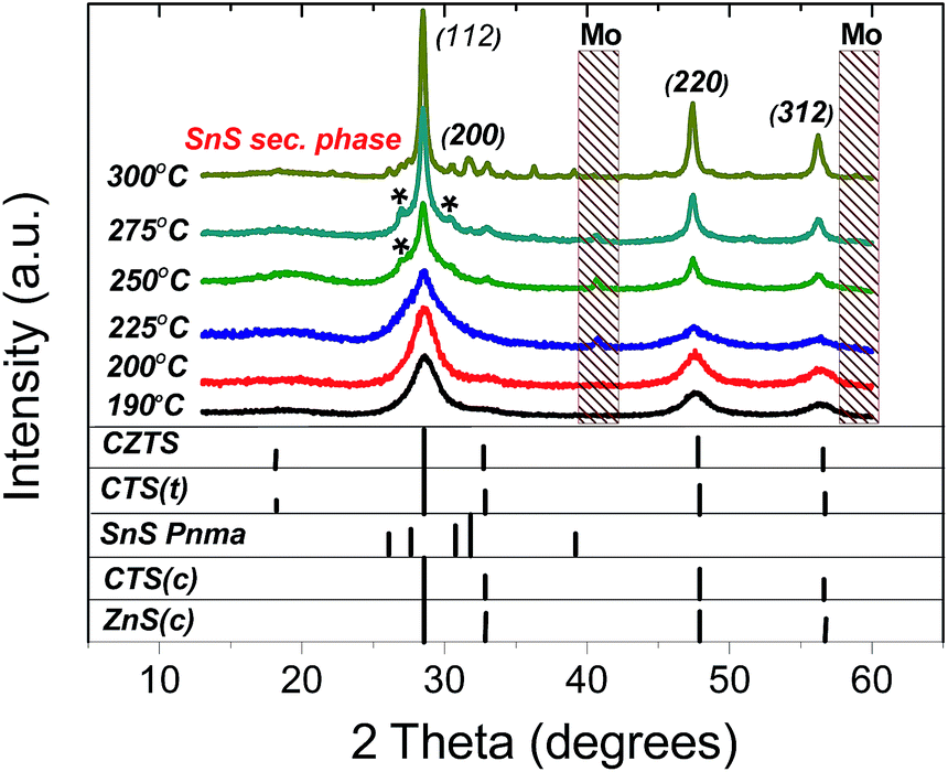 | ||
| Fig. 4 XRD patterns of as-synthesized nanocrystals with different injection temperatures compared to the reference patterns of cubic ZnS, cubic and tetragonal CTS, kesterite CZTS orthorhombic SnS. | ||
Due to the similar lattice parameters of tetragonal CTS (JCPDC 01-089-4714), cubic CTS (JCPDC 01-089-2877) and sphalerite ZnS (JCPDC 01-071-5975) the presence of these secondary phases cannot be excluded. No reflexes of the Cu2−xS phase have been observed. It can be seen that for the samples obtained at 250 °C and 275 °C injection temperatures two additional small peaks are present near the most intense (112) peak. This is a possible indication of the presence of stacking faults in the structure.38,39 For the sample synthesized at 300 °C, the secondary phase SnS with orthorhombic herzenbergite structure (JCPDS 01-071-3679) has been found. The line broadening observed in the XRD patterns is common for nanocrystal XRD patterns because of the finite crystallite size. The full width at half maximum (FWHM) of the diffraction peaks increases with decreasing crystallite size. The average coherence volume associated with the crystallite size can be estimated from FWHM of the most intensive diffraction peak (112) using the Scherrer formula under the assumption of spherical nanocrystals: D = Kλ/(βcosθ). The resulting estimates for average crystallite sizes are given in Table 2. The values for low temperature synthesis (190–225 °C) are in very good agreement with the TEM-derived nanocrystal sizes. Samples giving larger average particle sizes from XRD probably contain a fraction of NCs having diameter larger than the size determined from TEM which indicates the increasing polydispersity with temperature.
| Temperature | TEM average particle size, nm | XRD crystallite size (112), nm |
|---|---|---|
| 200 °C | 5.1 ± 0.9 | 5 |
| 225 °C | 3.9 ± 0.6 | 3.6 |
| 250 °C | 4.6 ± 0.7 | 2.9, 17 (15%) |
| 275 °C | 3.6 ± 0.7 (22 ± 5) | 3.1, 19.2 (30%) |
| 300 °C | — | 21.2 |
To gain further information on the kesterite as well as phase purity, Raman spectroscopy was employed. The Raman spectra of a CZTS nanocrystals obtained with different injection temperatures are presented in Fig. 5a (λexc = 632.8 nm).
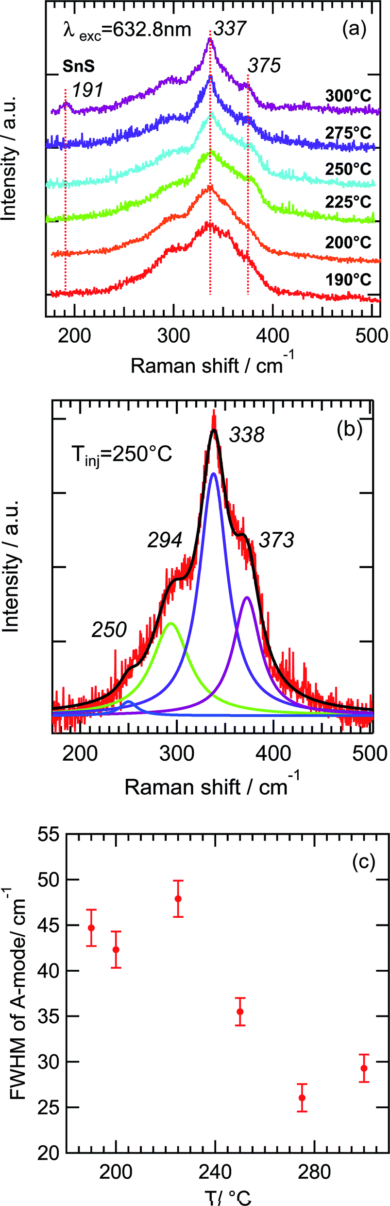 | ||
| Fig. 5 Raman spectra of CZTS NP synthesized at different injection temperatures (a). Deconvolution of the Raman spectrum of CZTS NP synthesized at 250 °C (b). FWHM of the A mode in dependence of injection temperature (c). | ||
The Raman spectra obtained for nanocrystals synthesized at different injection temperatures (190–300 °C) is characterized by the main broad peak located at 337 cm−1 and a shoulder at 375 cm−1, corresponding to the reported characteristic peaks for kesterite polycrystalline films.40
Also the shoulder at ∼300 cm−1 can be observed, which can be explained by CZTS modes at 289 and 302 cm−1.41 Despite of the very small size of nanocrystals no evidence of phonon confinement is observed probably because of the strain effect.42 As can be seen in Fig. 5a the increase of the injection temperature leads to a decrease of the FWHM of the main A mode at 337 cm−1. To evaluate the changes in FWHM with an increasing of Tinj we deconvolute Raman spectra with 4 Lorentzians located at about 250, 294, 338 and 373 cm−1. A representative example of this procedure is shown on Fig. 5b for Tinj = 250 °C. We determine that the FWHM of A mode varies from 45 to 25–30 cm−1 when Tinj increases from 190 to 300 °C (Fig. 5c).
Due to the broadening of peaks it is not possible to conclude about the presence of the CTS phase (peaks at 297 and 337 cm−1 for tetragonal CTS, 303 cm−1 and 355 cm−1 for cubic CTS, 318 cm−1 for orthorhombic CTS).40,43 To study CTS nanocrystals the identical synthesis with no Zn precursor at 225 °C was performed and Raman measurements were carried out to indicate the growth process (Fig. S4 in ESI†). For as-synthesized nanocrystals two main characteristic peaks at 291 cm−1 and 350 cm−1 of monoclinic CTS phase and 318 cm−1 of orthorhombic CTS phase were found.44 Therefore we exclude a CTS phase contribution to the shoulder at 300 cm−1 in Raman of CZTS NP.
At the highest injection temperature (300 °C) a peak45,46 at 191 cm−1 indicative of SnS nanocrystals has been observed (Fig. 5a), supporting our XRD results. To determine the presence of the ZnS phase, UV Raman scattering measurements (λexc = 325 nm) corresponding to near-resonant excitation for the ZnS phase were performed (Fig. S5 in ESI†). Only a very weak peak at 347 cm−1 is present for Tinj = 190, 200, 225 and 300 °C, with the highest intensity corresponding to Tinj = 200 °C. Thus the presence of the ZnS phase in some samples could be identified.
Optical transmission measurements were performed for all synthesized nanocrystals. In Fig. 6 the derived absorption is shown for different hot injection temperatures. Analysing the data further it is found that for the NCs synthesized between 225–275 °C a band gap of approximately 1.5 eV can be derived by modeling the absorption coefficient, however with the presence of very substantial subband gap absorption (Fig. S6 in ESI†).
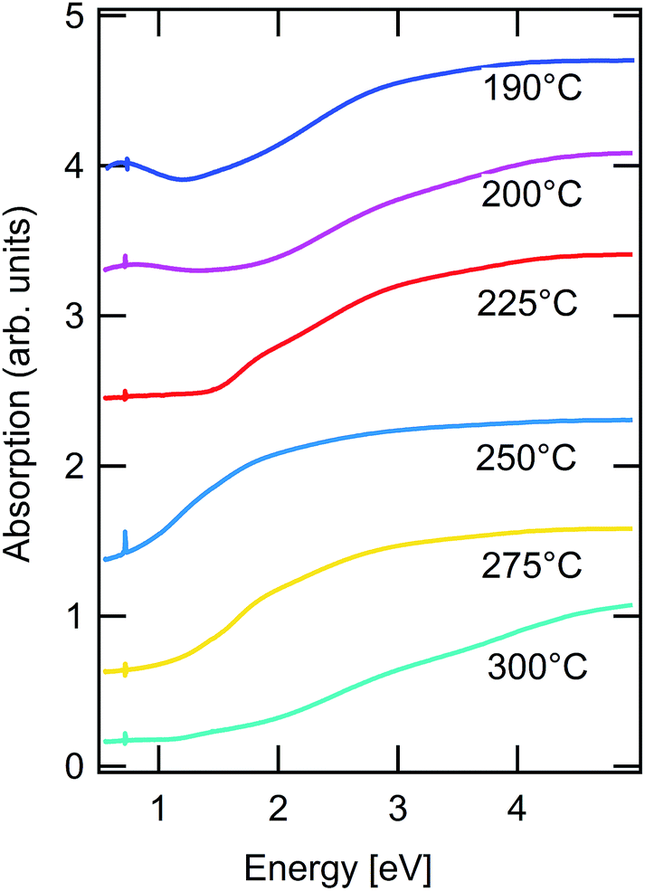 | ||
| Fig. 6 Absorption spectra of nanocrystals obtained at different injection temperatures. | ||
For the samples synthesized at injection temperatures of 190 °C and 200 °C a broad absorption peak in the near-infrared region can be observed. This can be a result of the localized surface plasmonic resonance (LSPR) possibly corresponding to a Cu2−xS phase.47 Since there is no evidence of the presence of Cu2−xS phase in XRD and Raman for this sample, formation of Cu2−xS–CZTS heterostructure due to the insufficient metals interdiffusion at this temperatures can be an explanation.48 The estimated band gap energy of 1.5 eV corresponds well to the value found for CZTS-bulk crystalline and polycrystalline material.49,50 The presence of strong bandtails can indicate the presence of defects at the surface and in the interior of the nanocrystals, which has previously been shown by high resolution transmission electron microscopy.51
Formation mechanism
To explore the growth of the CZTS nanocrystals monitoring of the reaction process has been performed using Raman spectroscopy (Fig. 7). Aliquots of the reaction solution were taken at certain time intervals, cleaned from the excess of organic compounds and drop casted on Mo glass.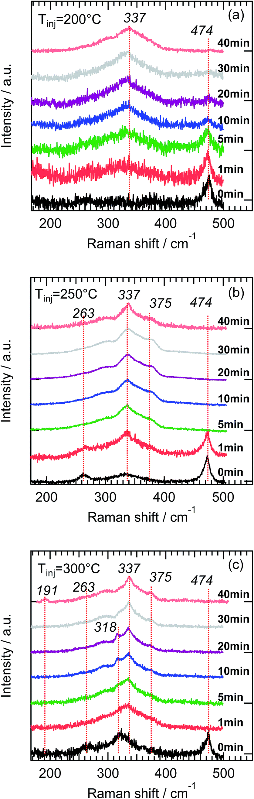 | ||
| Fig. 7 Evolution of Raman signal with increasing growth time at (a) 200 °C, (b) 250 °C and (c) 300 °C. | ||
The first aliquot was always taken immediately after injection (<2 s) of the sulfur precursor and indicated as 0 min time. For all injection temperatures a pronounced peak at 474 cm−1 and a weak mode at 263 cm−1 originating from Cu2−xS phase can be observed.52,53 The aliquots for this synthesis time have green color which is typical attributed in literature to formation of covellite CuS nanocrystals.54–56 With the exception of the sample synthesized at Tinj = 200 °C (Fig. 7a), Cu2−xS phases were not detected in other samples after 5 min of the reaction time (Fig. 7b and c) which is also characterized by changing of color of the aliquots from green to dark brown. We also observe that the Cu2−xS peak decreases faster with increasing injection temperature.
With the decrease of the Cu2−xS mode intensity, a broad peak centered at 337 cm−1 corresponding to the main kesterite A-mode emerges and becomes more pronounced during the growth time. The transition from the Cu2−xS phase to CZTS occurs at an earlier time for the higher injection temperatures (Fig. 7). We assume that this is due to a faster incorporation of Zn2+ and Sn4+ ions into the Cu2−xS crystal structure. However, at about 5–20 min after injection at 300 °C a new mode at 318 cm−1 (Fig. 7c) appears, which could be due to formation of the orthorhombic Cu3SnS4 phase.44 For the growth time >20 min we do not observe this Cu3SnS4 phase probably due to complete transformation to the CZTS phase. Note that at Tinj = 275 °C the Cu3SnS4 phase can be observed during the first minute of the synthesis (Fig. S7 in ESI†). The appearance of Cu3SnS4 at higher temperature is an indication that the competing ternary phase formation process delays complete formation of CZTS. Remarkably the Cu3SnS4 phase growth is influenced by both factors: Zn2+ ions presence and the growth temperature as the CTS formation can already start at Tinj = 225 °C without Zn precursor (Fig. S4 in ESI†). Overall, Fig. 8 shows NP formation path dependence on time and reaction temperature. Our data suggest that the growth time of about 40 min leads to complete CZTS NP formation in the temperature range of 190–300 °C.
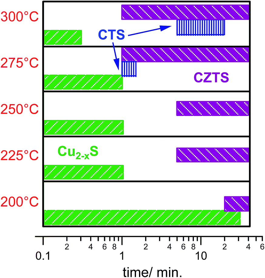 | ||
| Fig. 8 Scheme showing nanocrystals evolution with time and temperature obtained from Raman spectroscopy measurements on aliquots from reaction solution. | ||
Conclusions
In summary, we present a strategy for preparing small-sized (∼4–5 nm) CZTS kesterite nanocrystals which can be synthesized by the hot-injection method and Zn and Sn acetates as metal precursors. It was found that Cu/Sn and Zn/Sn ratios in as-synthesized nanocrystals strongly depend on the growth temperature. In particular for injection temperatures below 225 °C the reactivity of the Sn precursor is low which leads to Cu- and Zn-rich NCs.The CZTS nanocrystal formation mechanism at different temperatures has been studied by using Raman characterization of aliquots, taken during nanocrystal growth. We observed that Cu2−xS seeds form first, while the further incorporation of Zn2+ and Sn4+ ions into the structure strongly depends on the injection temperature. The time of complete transformation from the Cu2−xS phase into the CZTS phase decreases from about 40 to 1 min, when the growth temperature increases from 200 to 300 °C. The growth at high injection temperatures (∼275–300 °C) is characterised by the formation of a competing orthorhombic CTS phase during the first 20 min of the nanocrystal synthesis.
Acknowledgements
A. I. acknowledges support from the MATSEC graduate school at HZB.Notes and references
- N. J. Carter, W. C. Yang, C. K. Miskin, C. J. Hages, E. A. Stach and R. Agrawal, Sol. Energy Mater. Sol. Cells, 2014, 123, 189–196 CrossRef CAS.
- Q. Guo, H. W. Hillhouse and R. Agrawal, J. Am. Chem. Soc., 2009, 131, 11672–11673 CrossRef CAS PubMed.
- K. S. Cho, D. V. Talapin, W. Gaschler and C. B. Murray, J. Am. Chem. Soc., 2005, 127, 7140–7147 CrossRef CAS PubMed.
- Z. A. Peng and X. Peng, J. Am. Chem. Soc., 2001, 123, 1389–1395 CrossRef CAS.
- D. J. Milliron, S. M. Hughes, Y. Cui, L. Manna, J. Li, L.-W. Wang and A. P. Alivisatos, Nature, 2004, 430, 190–195 CrossRef CAS PubMed.
- T. K. Sau and A. L. Rogach, Adv. Mater., 2010, 22, 1781–1804 CrossRef CAS PubMed.
- D. Pan, X. Wang, Z. H. Zhou, W. Chen, C. Xu and Y. Lu, Chem. Mater., 2009, 21, 2489–2493 CrossRef CAS.
- H. Zhong, Y. Zhou, M. Ye, Y. He, J. Ye, C. He, C. Yang and Y. Li, Chem. Mater., 2008, 20, 6434–6443 CrossRef CAS.
- A. Singh, S. Singh, S. Levcenko, T. Unold, F. Laffir and K. M. Ryan, Angew. Chem., Int. Ed., 2013, 52, 9121–9124 Search PubMed.
- A. D. Collord and H. W. Hillhouse, Chem. Mater., 2015, 27, 1855–1862 CrossRef CAS.
- F. Zutz, C. Chory, M. Knipper, J. Parisi, I. Riedel, V. Izquierdo-Roca, X. Fontané and A. Pérez-Rodríguez, Phys. Status Solidi A, 2015, 212, 329–335 CrossRef CAS.
- M. D. Regulacio, C. Ye, S. H. Lim, M. Bosman, E. Ye, S. Chen, Q. H. Xu and M. Y. Han, Chem.–Eur. J., 2012, 18, 3127–3131 CrossRef CAS PubMed.
- C. Zou, L. Zhang, D. Lin, Y. Yang, Q. Li, X. Xu, X. Chen and S. Huang, CrystEngComm, 2011, 13, 3310 RSC.
- L. Arora, V. N. Singh, G. Partheepan, T. D. Senguttuvan and K. Jain, Appl. Nanosci., 2015, 1–10 Search PubMed.
- X. Lu, Z. Zhuang, Q. Peng and Y. Li, Chem. Commun., 2011, 47, 3141 RSC.
- A. Singh, H. Geaney, F. Laffir and K. M. Ryan, J. Am. Chem. Soc., 2012, 134, 2910–2913 CrossRef CAS PubMed.
- H. Zhou, W.-C. Hsu, H.-S. Duan, B. Bob, W. Yang, T.-B. Song, C.-J. Hsu and Y. Yang, Energy Environ. Sci., 2013, 6, 2822–2838 CAS.
- P. An, Z. Liang, X. Xu, X. Wang, H. Jin, N. Wang, J. Wang and F. Zhu, RSC Adv., 2015, 5, 6879–6885 RSC.
- Y. Qu, G. Zoppi, R. W. Miles and N. S. Beattie, Mater. Res. Express, 2014, 1, 045040 CrossRef.
- R. Ahmad, M. Brandl, M. Distaso, P. Herre, E. Spiecker, R. Hock and W. Peukert, CrystEngComm, 2015, 17, 6972–6984 RSC.
- Y. Kim, K. Woo, I. Kim, Y. S. Cho, S. Jeong and J. Moon, Nanoscale, 2013, 5, 10183–10188 RSC.
- S. Siebentritt, Thin Solid Films, 2013, 535, 1–4 CrossRef CAS.
- A. Khare, A. W. Wills, L. M. Ammerman, D. J. Norrisz and E. S. Aydil, Chem. Commun., 2011, 47, 11721–11723 RSC.
- G. Cao and Y. Wang, Nanostructures Nanomater. Synth. Prop. Appl., 2004, vol. 3, pp. 68–69 Search PubMed.
- S. K. Sinha, C. Srivastava, S. Sampath and K. Chattopadhyay, RSC Adv., 2015, 5, 4389–4395 RSC.
- W. S. Seo, H. H. Jo, K. Lee and J. T. Park, Adv. Mater., 2003, 15, 795–797 CrossRef CAS.
- H. Sigel, Angew. Chem., Int. Ed. Engl., 1975, 14, 394–402 CrossRef.
- G. Pearson, J. Am. Chem. Soc., 1963, 85, 3533–3539 CrossRef.
- G. N. Lewis, Chem. Cat. Co., 1923, 142 Search PubMed.
- R. G. Pearson, J. Chem. Educ., 1968, 45, 581 CrossRef CAS.
- J. M. R. Tan, Y. H. Lee, S. Pedireddy, T. Baikie, X. Y. Ling and L. H. Wong, J. Am. Chem. Soc., 2014, 136, 6684–6692 CrossRef CAS PubMed.
- V. T. Tiong, J. Bell and H. Wang, Beilstein J. Nanotechnol., 2014, 5, 438–446 CrossRef PubMed.
- I. D. Olekseyuk, I. V. Dudchak and L. V. Piskach, J. Alloys Compd., 2004, 368, 135–143 CrossRef CAS.
- L. E. Valle Rios, K. Neldner, G. Gurieva and S. Schorr, J. Alloys Compd., 2016, 657, 408–413 CrossRef CAS.
- S. Chen, J. H. Yang, X. G. Gong, A. Walsh and S. H. Wei, Phys. Rev. B: Condens. Matter Mater. Phys., 2010, 81, 245204 CrossRef.
- J. Just, C. M. Sutter-Fella, D. Lützenkirchen-Hecht, R. Frahm, S. Schorr and T. Unold, Phys. Chem. Chem. Phys., 2016, 18, 15988–15994 RSC.
- R. Vallée, M. Wautelet, J. P. Dauchot and M. Hecq, Nanotechnology, 2001, 12, 68–74 CrossRef.
- H. Rodriguez-Alvarez, N. Barreau, C. A. Kaufmann, A. Weber, M. Klaus, T. Painchaud, H. W. Schock and R. Mainz, Acta Mater., 2013, 61, 4347–4353 CrossRef CAS.
- N. Kattan, B. Hou, D. J. Fermín and D. Cherns, Applied Materials Today, 2015, 1, 52–59 CrossRef.
- P. A. Fernandes, P. M. P. Salomé and A. F. Da Cunha, J. Alloys Compd., 2011, 509, 7600–7606 CrossRef CAS.
- T. Jawhari, M. Dimitrievska, A. Fairbrother and E. Saucedo, Appl. Phys. Lett., 2014, 021901, 1–5 Search PubMed.
- M. Dimitrievska, A. Fairbrother, A. Pérez-Rodríguez, E. Saucedo and V. Izquierdo-Roca, Acta Mater., 2014, 70, 272–280 CrossRef CAS.
- P. A. Fernandes, P. M. P. Salomé and A. F. da Cunha, J. Phys. D: Appl. Phys., 2010, 43, 215403 CrossRef.
- D. M. Berg, R. Djemour, L. Gütay, S. Siebentritt, P. J. Dale, X. Fontane, V. Izquierdo-Roca and A. Pérez-Rodriguez, Appl. Phys. Lett., 2012, 100, 192103 CrossRef.
- S. Sohila, M. Rajalakshmi, C. Ghosh, A. K. Arora and C. Muthamizhchelvan, J. Alloys Compd., 2011, 509, 5843–5847 CrossRef CAS.
- L. S. Price, I. P. Parkin, A. M. E. Hardy, R. J. H. Clark, T. G. Hibbert and K. C. Molloy, Chem. Mater., 1999, 11, 1792–1799 CrossRef CAS.
- I. Kriegel, C. Jiang, J. Rodríguez-Fernández, R. D. Schaller, D. V. Talapin, E. Da Como and J. Feldmann, J. Am. Chem. Soc., 2012, 134, 1583–1590 CrossRef CAS PubMed.
- H.-C. Liao, M.-H. Jao, J.-J. Shyue, Y.-F. Chen and W.-F. Su, J. Mater. Chem. A, 2013, 1, 337–341 CAS.
- K. Ito and T. Nakazawa, Jpn. J. Appl. Phys., 1988, 27, 2094–2097 CrossRef CAS.
- K. Hönes, E. Zscherpel, J. Scragg and S. Siebentritt, Phys. B, 2009, 404, 4949–4952 CrossRef.
- N. A. Kattan, I. J. Griffiths, D. Cherns, D. J. Fermín, D. Mitzi, O. Gunwan, T. Todorov, D. Barkhouse, A. Nagaoka, H. Miyake, T. Taniyama, K. Yoshino, S. Shen, A. Walsh, X. Gong, S. Wei, S. Schorr, H. J. Hoebler, M. Tovar, T. Gokmen, O. Gunawan, T. Todorov, D. Mitzi, T. Gershon, B. Shin, N. Bojarczuk, T. Gokmen, S. Lu, S. Guha, T. Washio, H. Nozaki, T. Fukano, T. Motohiro, K. Jimbo, H. Katagiri, J. Scragg, J. Larsen, M. Kumar, C. Persson, J. Sendler, S. Siebentritt, C. P. Björkman, R. Haight, X. Shao, W. Wang, D. Mitzi, N. Kattan, B. Hou, D. Fermín, D. Cherns, B. Mendis, M. Shannon, M. Goodman, J. Major, R. Claridge, D. Halliday, K. Durose, B. Hou, D. Benito-Alifonso, N. Kattan, D. Cherns, M. Galan, D. Fermín, S. J. Pennycook, D. E. Jesson, S. Chen, J. Yang, X. Gong, A. Walsh and S. Wei, Nanoscale, 2016, 8, 14369–14373 RSC.
- B. Minceva-Sukarova, M. Najdoski, I. Grozdanov and C. J. Chunnilall, J. Mol. Struct., 1997, 410–411, 267–270 CAS.
- S.-Y. Wang, W. Wang and Z.-H. Lu, Mater. Sci. Eng., B, 2003, 103, 184–188 CrossRef.
- A. Dutta and S. K. Dolui, Mater. Chem. Phys., 2008, 112, 448–452 CrossRef CAS.
- F. F. Castillón-Barraza, M. H. Farías, J. H. Coronado-López, M. A. Encinas-Romero, M. Pérez-Tello, R. Herrera-Urbina and A. Posada-Amarillas, Adv. Sci. Lett., 2011, 4, 596–601 CrossRef.
- L. Fotouhi and M. Rezaei, Microchim. Acta, 2009, 167, 247–251 CrossRef CAS.
Footnote |
| † Electronic supplementary information (ESI) available: TEM image for the sample obtained with lower amount of oleylamine; TEM images of Cu2−xS, CTS, ZnS and SnxSy nanocrystals obtained with same reaction conditions as CZTS nanocrystals; temperature dependence of Cu/Sn and Zn/Sn ratios of NCs synthesized with weight-in ratio of Zn/Sn = 1.2; evolution of Raman signal of CTS nanocrystals with increasing of the growth time at 225 °C; Raman spectrum of nanocrystals synthesized at different injection temperatures measured with UV excitation laser; absorption coefficient of CZTS nanocrystals in conjunction with model. See DOI: 10.1039/c6ra28588k |
| This journal is © The Royal Society of Chemistry 2017 |