DOI:
10.1039/C6RA25426H
(Paper)
RSC Adv., 2017,
7, 4179-4189
A study on the surface quality and brittle–ductile transition during the elliptical vibration-assisted nanocutting process on monocrystalline silicon via molecular dynamic simulations
Received
18th October 2016
, Accepted 12th December 2016
First published on 16th January 2017
Abstract
Molecular dynamic (MD) simulation method was applied to investigate the surface quality and brittle–ductile transition of monocrystalline silicon with a diamond tool during the elliptical vibration-assisted nanocutting (EVANC) and traditional nanocutting process. In the simulations, the interaction between silicon atoms in the specimen was modeled by the Tersoff potential, whereas the Morse potential was for the description of the interactions between silicon atoms in the specimen and carbon atoms in the diamond tool. In this study, we discovered that EVANC not only changed the brittle-mode cutting into the ductile-mode cutting, but also made the phase transformation layer thinner than that in the traditional nanocutting, which leads to a better surface finish and a large rate of removal of materials. Herein, stress analysis showed that the stress-affected region of the workpiece processed by EVANC was smaller than that of the workpiece processed by the traditional nanocutting. The temperature also increased during the EVANC process. This may soften the silicon material and make the cutting easier. In EVANC, the tangential force and normal force decreased because of the change in the brittle–ductile transition. From the simulation results, EVANC removed the material in the ductile mode, which could increase the removal rate, improve the surface finish, and decrease the cutting force to reduce the tool wear. In conclusion, EVANC has positive effects on the machinability and surface finish of the silicon material.
1. Introduction
Monocrystalline silicon is widely used in electronic products, industrial automation, computer systems, and precision optics.1,2 To ensure high surface finish quality and intricate features of the optical and semiconductor productions, an ultra-precise machining method should be performed on silicon. However, severe subsurface damage and cracks can be generated through the ordinary machining methods. Removing the amorphous layer from the silicon workpiece surface is also difficult.3 In the machining process, a larger cutting force leads to severe tool wear as well. Therefore, a practicable machining method to solve these problems is required. Elliptical vibration-assisted machining (EVAM), an emerging method in the ultra-precise machining, has been developed into a reliable method for the hard material processing. In EVAM, the tool tip is driven in an elliptical motion to improve the fabrication process.4–6 Experiments investigated in the research studies have shown that EVAM can reduce the cutting force.7 Shamoto et al. carried out a detailed research on the cutting forces in EVAM. They found that the maximum instantaneous force in EVAM is smaller than that in the 1D VAM and traditional machining. They also found that the thrust force reverses the direction for the part of each cutting cycle.8 Unfortunately, no research study has reasonably explained the experimental phenomena. Another advantage of EVAM is the surface finish quality improvement of the workpiece.9 Uhlmann et al. performed single grain scratch tests on ceramic. They indicated that the vibration-assisted grinding can improve the surface finish quality and the material removal rate was increased without causing superproportional subsurface damages.10 Moreover, EVAM is reported as a valid machining method to change the brittle-mode cutting into the ductile-mode cutting.11–13 Negishi et al. performed the groove cutting experiments on silicon and made the ductile regime machining of the brittle materials. They maintained ductile cutting to a depth of 3.5 μm with an acceptable surface finish.7 Liang et al. conducted the scratching experiments on sapphire in the absence and presence of the elliptical ultrasonic vibration. The results they obtained from the SEM images suggest that the elliptical ultrasonic-assisted scratching can change the brittle-mode cutting into the ductile-mode cutting at the critical depth of the cut.14 However, why an elliptical vibration-assisted scratching can cause the brittle–ductile transition is still a debated issue.
Theoretical analysis has been made to explain the machining mechanism. Molecular dynamic (MD) simulation is an effective method on the atomic scale. Some researchers have performed the MD simulations to explain why the brittle–ductile transition occurs while cutting the hard materials such as monocrystalline silicon and silicon carbide (SiC). Zhang et al. carried out investigations on monocrystalline silicon through MD nanocutting simulations and found that the extremely small cutting depth, large cutting radius, and negative rake angle had positive effects on the removal of silicon ductile-mode.15 Xiao et al. studied the process of cutting the silicon carbide workpiece with a diamond tool through the MD cutting simulations. They concluded that increasing the cutting depth could change the ductile-mode cutting into the brittle-mode cutting. Tensile stress increases with the increasing cutting depth and the tensile stress might result in pre-existing cracks.16
Although various theoretical analyses on the traditional nanocutting have been applied in the investigations, few research studies on EVAM have been carried out. To find out the mechanism of EVAM in the atomic scale on the brittle material like silicon, we first designed the MD simulation model to investigate the differences between the traditional nanocutting and elliptical vibration-assisted nanocutting (EVANC). Comparisons were carried out between the simulations in terms of chip formation, residual topography, Von Mises shear stress, atom flow field, and cutting force.
2. Simulation method
2.1. MD simulation model
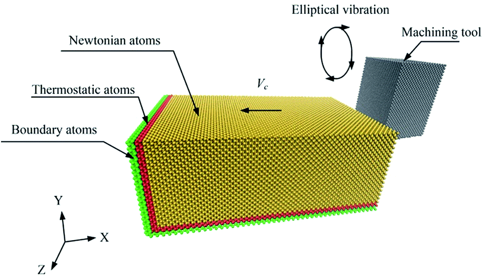
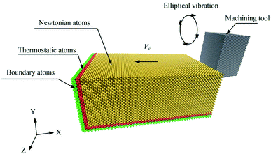
In the simulation, we constructed a three-dimensional MD nanocutting model, which is demonstrated in Fig. 1.
 |
| | Fig. 1 Three-dimensional MD simulation model. | |
The model consists of two parts, a diamond cutting tool and a monocrystalline silicon specimen. The size of the specimen is 25.00 nm × 9.00 nm × 16.00 nm along the X, Y, and Z directions. The specimen consists of 196![[thin space (1/6-em)]](https://www.rsc.org/images/entities/char_2009.gif) 466 silicon atoms and the diamond cutting tool is made up of 23392 carbon atoms. For the diamond tool, the rake angle is 0°, the clearance angle is 7°, and the tool radius is 1.0 nm. The hardness of diamond is much greater than that of silicon,17,18 and thus it can be assumed that the diamond tool does not deform in the simulation process. Therefore, the diamond tool is regarded as a rigid body. The X–Y plane of the specimen is constructed with a free surface because the specimen is cut in the X-direction. The silicon atoms in the simulations are categorized into three parts in the specimen, namely, Newtonian atoms, thermostat atoms, and boundary atoms. The function of the boundary atoms is to reduce the boundary effects and maintain the proper symmetry of the lattice. The thermostat atoms are categorized to make sure there is reasonable outward heat conduction away from the machined zone. The motions of the Newtonian atoms and thermostat atoms are governed by Newton's second law. Moreover, to reduce the simulation scale, the periodic boundary condition is set along the Z-direction.19 In the simulations, a large-scale atomic/molecular massively parallel simulator (LAMMPS), which was developed by Plimpton, was used to perform the MD simulation.20 Visual molecular dynamics (VMD), the open visualization tool (OVITO), and AtomEye were also used to visualize the results of the simulations.21–23
466 silicon atoms and the diamond cutting tool is made up of 23392 carbon atoms. For the diamond tool, the rake angle is 0°, the clearance angle is 7°, and the tool radius is 1.0 nm. The hardness of diamond is much greater than that of silicon,17,18 and thus it can be assumed that the diamond tool does not deform in the simulation process. Therefore, the diamond tool is regarded as a rigid body. The X–Y plane of the specimen is constructed with a free surface because the specimen is cut in the X-direction. The silicon atoms in the simulations are categorized into three parts in the specimen, namely, Newtonian atoms, thermostat atoms, and boundary atoms. The function of the boundary atoms is to reduce the boundary effects and maintain the proper symmetry of the lattice. The thermostat atoms are categorized to make sure there is reasonable outward heat conduction away from the machined zone. The motions of the Newtonian atoms and thermostat atoms are governed by Newton's second law. Moreover, to reduce the simulation scale, the periodic boundary condition is set along the Z-direction.19 In the simulations, a large-scale atomic/molecular massively parallel simulator (LAMMPS), which was developed by Plimpton, was used to perform the MD simulation.20 Visual molecular dynamics (VMD), the open visualization tool (OVITO), and AtomEye were also used to visualize the results of the simulations.21–23
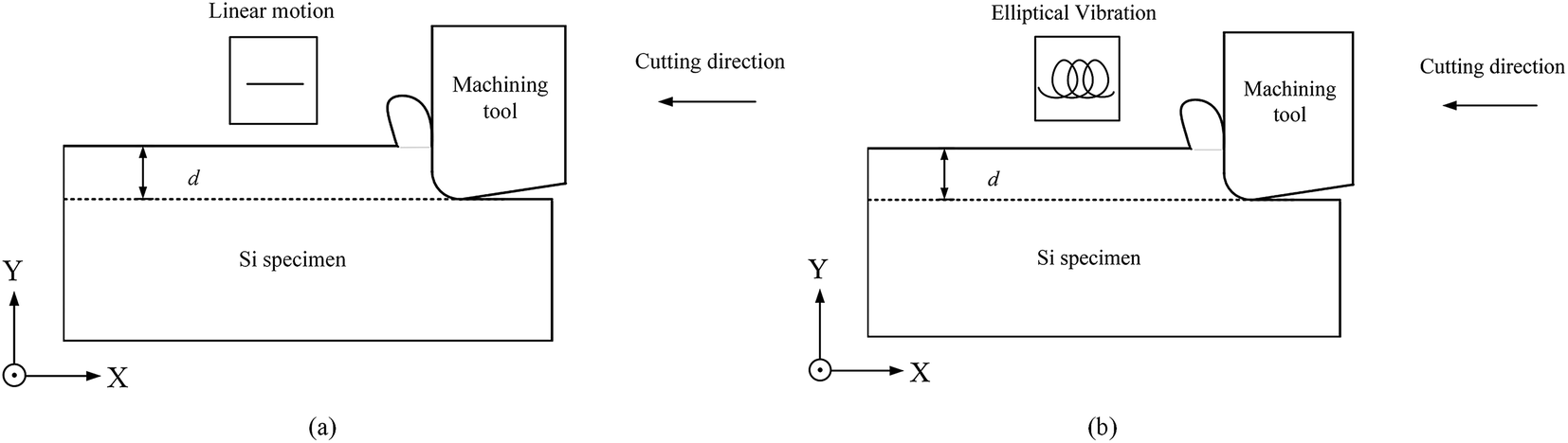
Fig. 2 shows the procedure of simulation. The monocrystalline silicon specimen is machined along the [100] direction in the (010) surface. The tool in EVANC vibrates periodically as compared to that in the traditional nanocutting. The diamond tool does “Elliptical Vibration Cutting”, which synchronizes the X and Y directional vibration.1 In the simulations, the X direction is the cutting direction and the Y direction is perpendicular to the machined surface. The cutting edge forms an elliptical locus in the X–Y plane in each vibration cycle. The cutting velocity was set at 50 m s−1 to reduce the time and amount of computation.24 To match the cutting speed, the vibration period was 25 ps.25 The amplitudes of the diamond tool in the X and Y directions were 2.0 nm and 1.0 nm, respectively. The simulation was at the initial temperature of 296 K to simulate the room temperature. Parameters used in the simulation model are listed in Table 1.
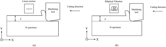 |
| | Fig. 2 Schematic of the nanocutting process. (a) Traditional nanocutting and (b) elliptical vibration-assisted nanocutting. | |
Table 1 Parameters applied in the simulation model
| Dimensions of the silicon specimen |
25.00 nm × 9.00 nm × 16.00 nm |
| Number of silicon atoms in the specimen |
196466 |
| Number of carbon atoms in the diamond tool |
23392 |
| Rake angle of the diamond tool |
0° |
| Clearance angle of the diamond tool |
7° |
| Diamond tool edge radius |
1.0 nm |
| Cutting depth |
1.5 nm |
| Specimen machining surface |
(010) |
| Cutting direction |
[100] |
| Equilibration temperature |
296 K |
| Cutting speed |
v = 50 m s−1 |
| Cutting distance |
20.0 nm |
| Time step |
1 fs |
2.2. Selection of the potential energy function
A proper interaction potential function determines the accuracy of the simulation process and the results of an MD simulation. There are two types of atoms simulated in the MD simulation: silicon atoms and carbon atoms. Therefore, three different atomic interactions should be considered. The first interaction is between silicon atoms (Si–Si), the second interaction is between carbon atoms (C–C), and the third interaction is between silicon atoms and carbon atoms (Si–C).
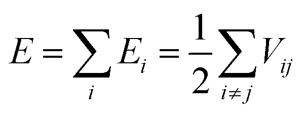
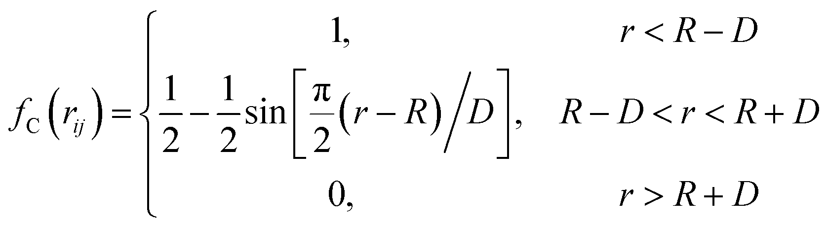
Silicon–silicon interactions and carbon–carbon interactions can be well described by the Tersoff potential;26–28 hence, the Tersoff potential was adopted to describe the silicon–silicon interaction in the simulations. The formulas for the Tersoff potential are presented as follows:
| |
 | (1) |
| | |
Vij = fc(rij)[aijfR(rij) + bijfA(rij)]
| (2) |
| | |
fR(rij) = Aexp(−λijr)
| (3) |
| | |
fA(rij) = −Bexp(−μijr)
| (4) |
| |
 | (5) |
| | |
bij = (1 + βiniζijni)−1/2ni
| (6) |
| |
 | (7) |
| | |
g(θ) = 1 + c2/d2 − c2/[d2 + (h − cosθ)2]
| (8) |
| | |
aij = (1 + αnηijn)−1/2n
| (9) |
| |
 | (10) |
E and Vij represent the total energy and the bond energy of all the atomic bonds, respectively. i, j, and k are the atoms of the system, rij is the bond length of the atoms i and j, bij is the bond order term, θijk represents the angle between bond ij and bond ik, repulsive pair potential and attractive pair potential are indicated by fR and fA, fC is a smooth cut-off function to limit the range of the potential, and ξij represents the other bonds to atom i besides the bond ij. Other parameters are cited from a reference, listed in Table 2.
Table 2 Parameters used in the Tersoff potential for silicon28
| Parameter |
Silicon–silicon |
| A (eV) |
1830.8 |
| B (eV) |
471.18 |
| λ (Å−1) |
2.4799 |
| μ (Å−1) |
1.7322 |
| α |
0.0 |
| β |
1.1000 × 10⁻⁶ |
| n |
0.78734 |
| c |
1.0039 × 10⁵ |
| d |
1.6217 × 10 |
| h |
−0.59825 |
| λ3 (Å−1) |
1.7322 |
| R (Å) |
2.85 |
| D (Å) |
0.15 |
The Morse potential is used to describe the interactions between the carbon atoms in the tool and the silicon atoms in the specimen. The potential is expressed as follows:29
| | |
V(rij) = D(e−2α(rij−r0) − 2e−α(rij−r0))
| (11) |
where
V(
rij) is the pair-potential and
D,
α, and
r0 correspond to the cohesion energy, the elastic modulus, and the atomic distance at equilibrium, respectively. The values of the potential parameters are
D = 0.435 eV,
α = 46.487 nm
−1, and
r0 = 0.19475 nm. The parameters are cited from a
ref. 29.
3. Simulation results and discussion
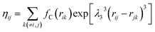
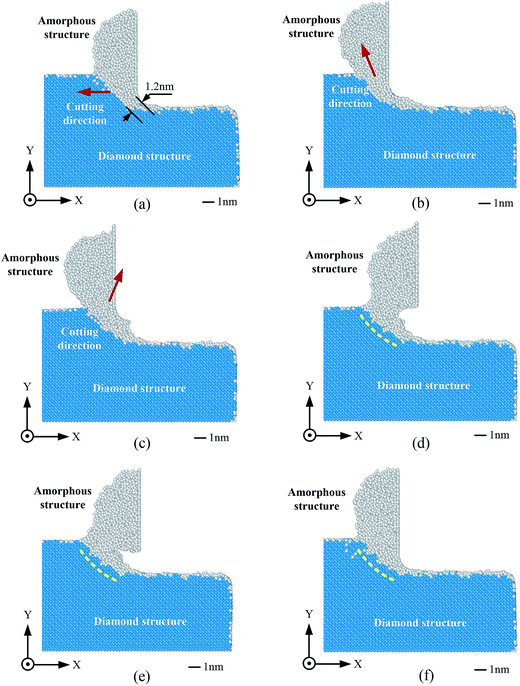
The mechanisms of EVANC and traditional nanocutting require to be compared before analyzing the other properties. Fig. 3 shows the atomic configuration within one period of oscillation in EVANC and Fig. 4 gives the relative cutting distance in the traditional nanocutting.
 |
| | Fig. 3 Cross-sectional view of EVNAC in one period of oscillation from the distance of 11.25 nm. (a)–(f) show one complete period of EVANC. | |
 |
| | Fig. 4 Cross-sectional view of the traditional nanocutting process from the distance of 11.25 nm. (a)–(f) and Fig. 3(a)–(f) are in time consistence. | |
Fig. 3(a)–(f) gives the EVANC process in one complete period. In EVANC, the blue part, as shown in the figure, represents the diamond structure and the white part is the amorphous structure. In Fig. 3(a), the tool is at the lowest position and the cutting direction is along the negative direction of the X-axis. The thickness of the amorphous structure between the tool nose and the unprocessed diamond structure is 1.2 nm. The cutting direction changes during the cutting process. As Fig. 3(b) shows, material was swept up along the direction of tool movement to form chips, and the cutting process in EVANC has little effect on the subsurface. The workpiece surface is a free surface and the atoms would not get much resistance to form the chips. There is also a period in EVANC when the tool is away from the main silicon workpiece, and the region to be machined doesn't change its morphology (marked by yellow dotted lines in Fig. 3(d)–(f)). Moreover, there are some differences between EVANC and EVAM. As the diamond tool moves away from the workpiece, the chip in EVANC adheres to the cutting tool. There are two reasons for this: first, on the atomic scale, silicon atoms and carbon atoms have a great gravitational effect, which is described by the Tersoff potential;28 second, higher cutting speed leads to higher temperature and this makes the chip softer. At the initial cutting period, the chip mass is quite small and it has the tendency to adhere to the diamond tool.
Fig. 4(a)–(f) shows the continuous process of traditional nanocutting for comparison with EVANC. The cutting tool moves along the negative direction of the X-axis and the direction does not change during the cutting process. The thickness of the amorphous structure between the tool nose and the unprocessed diamond structure is 1.8 nm, as shown in Fig. 4(a), which is thicker than that in EVANC. During the traditional nanocutting process, a thick amorphous layer can be found under the diamond tool (highlighted by the yellow dotted line). This phenomenon may result from the unchanged cutting direction during the traditional nanocutting. This cutting mode leads to the formation of a compression-induced region and the compression stress results in the subsurface layer. Detailed analysis is discussed hereinafter.
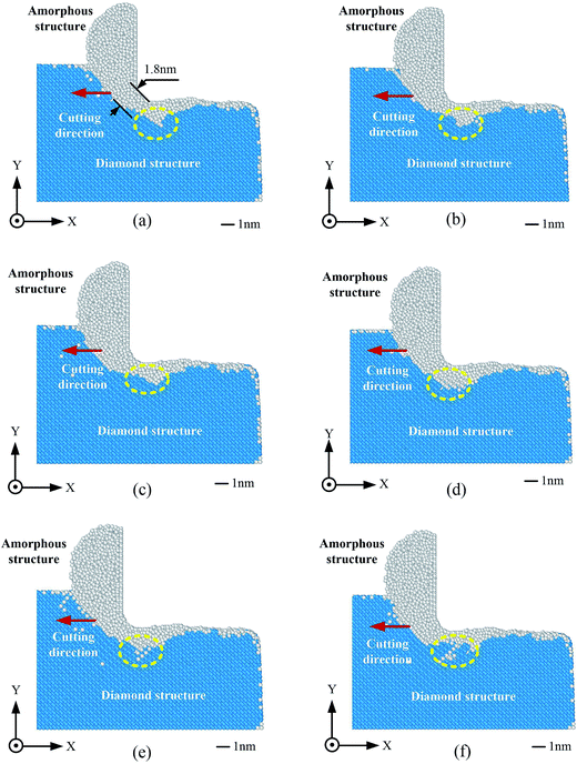
3.1. Analysis of the phase transition via EVANC and traditional nanocutting
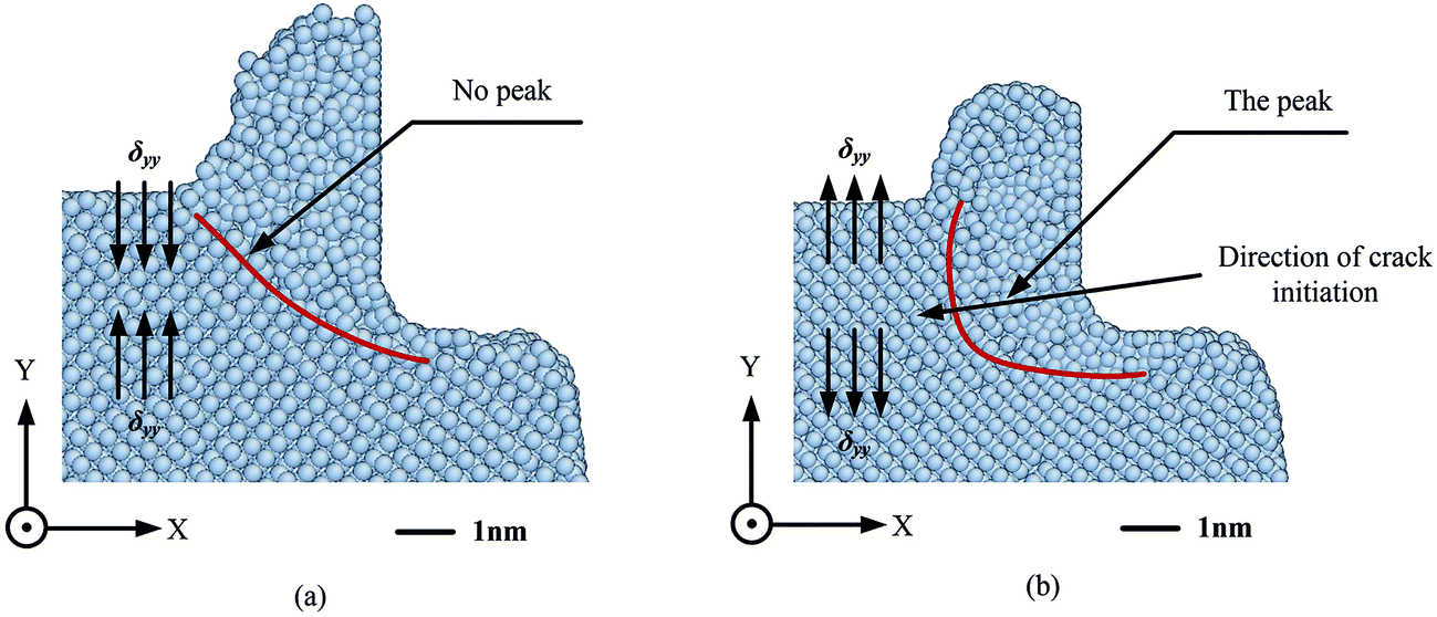
Fig. 5 shows the cross-sectional view of the deformation of the workpiece in the chip formation zone and Fig. 6 gives the δyy stress analysis in the chip formation zone. The deformation zone in the specimen is marked by the red bold line in Fig. 5. As Fig. 5(a) shows, it is obvious, based on the atomic arrangement, that there is no peak induced by EVANC in the chip formation zone. Atoms in the amorphous phase region are pressed and moved by the shear stress to the free surface. Hence, the material removed by EVANC is regarded as ductile-mode nanocutting.
 |
| | Fig. 5 Cross-sectional view of the deformation of the specimen in the chip formation zone when for the tool Rt = 1.0 nm and d = 1.5 nm. (a) Elliptical vibration-assisted nanocutting and (b) traditional nanocutting. | |
 |
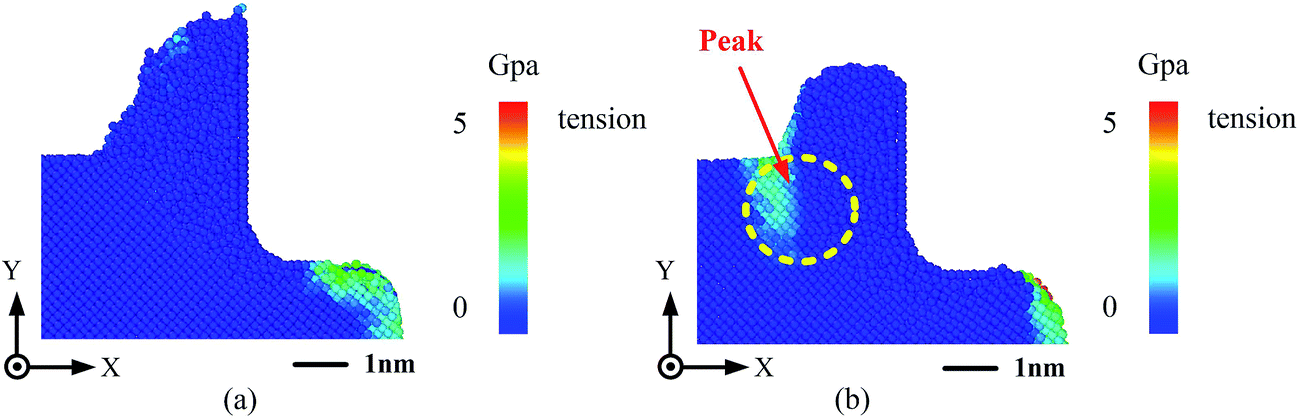
| | Fig. 6 Cross-sectional view of the δyy stress field in the chip formation zone when the tool Rt = 1.0 nm and d = 1.5 nm. (a) Elliptical vibration-assisted nanocutting and (b) traditional nanocutting. | |
However, the peak can be clearly seen in Fig. 5(b). The peak is formed as the cutting tool moves forward. The position of the peak is in front of the point of the rake face and tool edge. As is marked by the yellow dotted circle in Fig. 6(b), the peak deformation zone expands ahead, which results in a tensile stress state in front of the peak zone on the silicon specimen. The material tends to split, which can lead to crack generation. Therefore, the material shows the brittle-mode cutting through the traditional cutting.
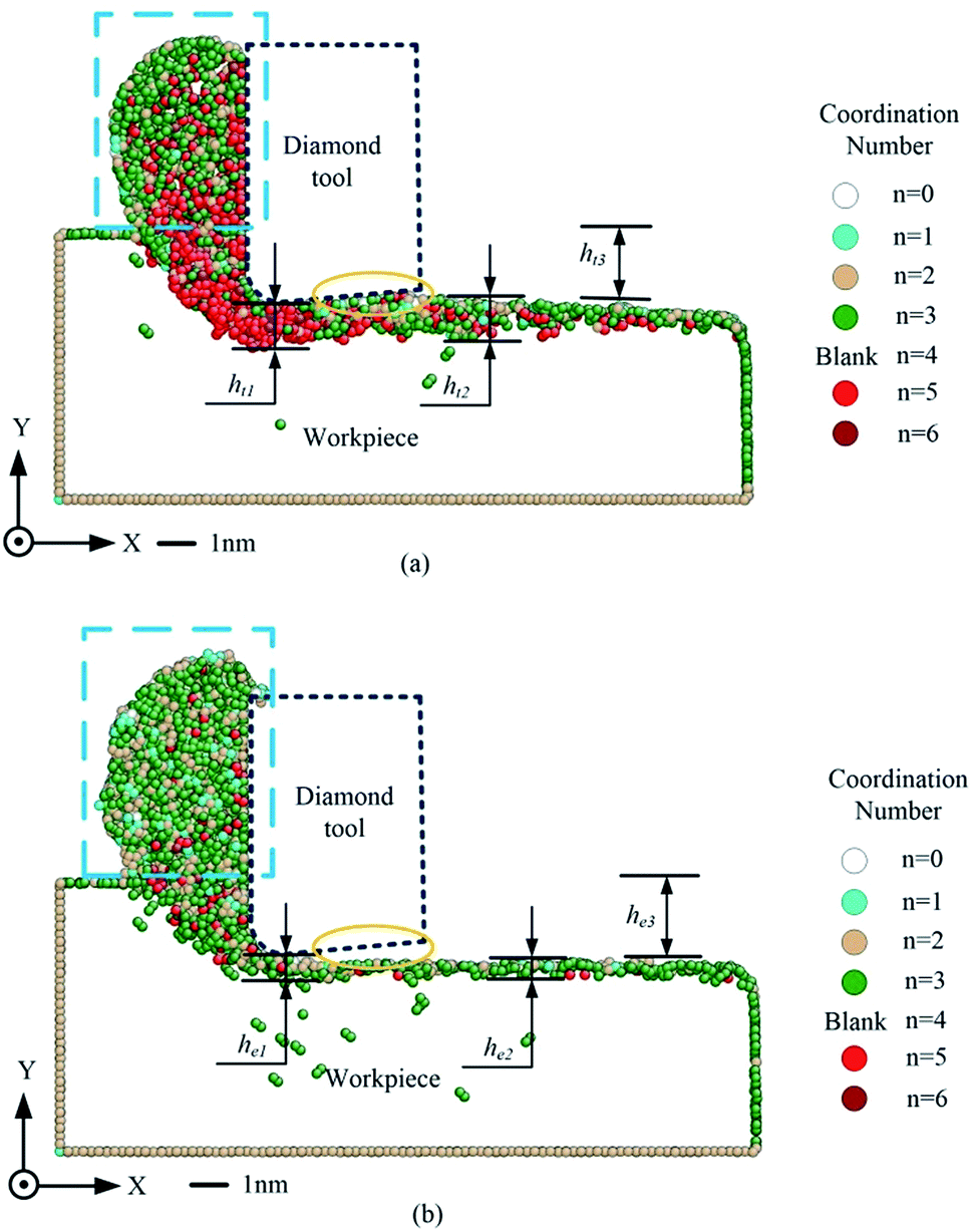
3.2. Analysis of the surface finish via EVANC and traditional nanocutting
Fig. 7 is the cross-sectional view of the phase transformation of the monocrystalline silicon atoms during the cutting process. The coordination numbers in the specimen are applied to analyze the range of the phase transformation using AtomEye. Coordination numbers and colors are listed, and the atoms where the coordination number is equal to four (c-silicon) are eliminated to reduce the interference of observation. Fig. 7(a) is obtained from the traditional nanocutting process and molecular dynamic process. The chip and cutting induced region are composed of amorphous silicon atoms. The silicon atoms are mainly amorphous silicon mixed with β-silicon (n = 6). This simulation result can be described as follows: the diamond cubic four-coordinated c-silicon transforms into six-coordinated β-silicon through the traditional nanocutting process. However, in Fig. 7(b), only a small amount of c-silicon transforms into β-silicon. In the traditional nanocutting process, the movement of the cutting tool is linear. Some silicon atoms in front of the tool move downward because of the tensile stress analyzed in Fig. 7(b). The atoms are pressed by the cutting tool and transformed from c-silicon to β-silicon. As the tool passes by, the stress of the silicon atoms is released and some of the amorphous silicon recovers to the original structure. In EVANC, the trajectory of the cutting tool is elliptical and the direction of motion changes over time. Hence, few atoms are pressed downward to become the amorphous layer of the machined surface and the amount of β-silicon is small. The height of the affected silicon layer being processed is marked h1, the height of the affected silicon layer processed is marked h2, and the thickness of the material removed is marked h3. It is clear that the thickness of the amorphous layer being processed via traditional nanocutting is larger than of that processed by EVANC, namely ht1 > he1. This can prove that more silicon atoms are pressed by the tool to change the phase due to the unchanged direction of the tool motion in the traditional nanocutting. Although there is material recovery in the processed surface, the affected layer of the traditional nanoscratching is still thicker than that of EVANC, namely ht2 > he2. Hence, the thickness of the affected layer on the machined surface can be decreased through EVANC. According to the investigation of Shi et al., the affected layer can decrease the hardness of the silicon workpiece surface.30 Therefore, EVANC can improve the surface quality. As is shown in the area highlighted by the yellow line in Fig. 7(a), there is a clear elastic recovery in the traditional nanocutting process. The recovery comes from the strain (ε) generated from the stress (σ) unloading. Hooke's law describes this relationship in terms of stiffness C.31
 |
| | Fig. 7 Cross-sectional views of the phase transformation atoms during the nanocutting process. (a) Traditional nanocutting and (b) elliptical vibration-assisted nanocutting. | |
In the simulations, normal force on the workpiece is along the [010] direction and thus the stiffness C can be regarded as Young's modulus on the [010] direction E010. Therefore, the formula (13) can be written as follows:
| |
 | (13) |
The value of stress (σ) results from the normal force of the cutting tool, shown in Fig. 7. In traditional nanocutting, the normal force is larger than that of EVANC. Therefore, the strain from the traditional cutting is smaller than that from EVANC, which results in the large distance of elastic recovery.
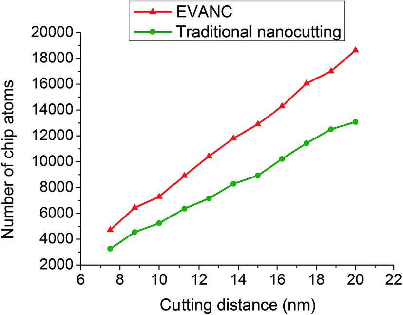
The recovered material contacts the clearance face, which leads to a clearance face tool wear through nanocutting. However, in Fig. 7(b), there is a gap between the tool and the cutting-induced surface. This can avoid the friction between the clearance face and the workpiece, which avoids the tool wear. Moreover, the material removal rate is different. It can be observed that the amount of material removed through EVANC is more than that removed through the traditional cutting because ht3 < he3. The number of atoms in the chip zone (highlighted by the blue dashed frame) can more clearly define the situation. The number of chip atoms in EVANC, as shown in Fig. 8, is larger than that in the traditional nanocutting, which means that at the same cutting depth and cutting distance, more material was removed through EVANC; therefore, the material removal rate of EVANC is greater.
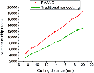 |
| | Fig. 8 Number of chip atoms at different cutting distances. | |
3.3. Analysis of Von Mises shear stress via the elliptical vibration-assisted nanocutting and traditional nanocutting
The equivalent von Mises stress equation is a yield criterion and is used to determine if the yield stress state at the onset of plastic yielding has occurred in a solid element.32 The stress is expressed as follows:| |
 | (14) |
where σ1, σ2, and σ3 are the principal stresses.
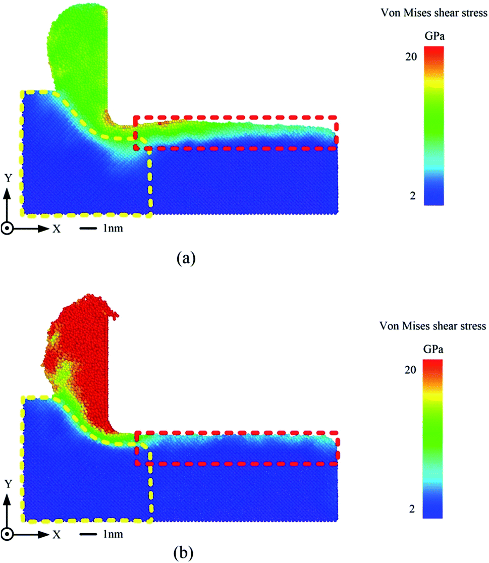
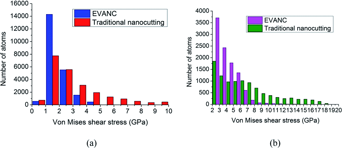
Fig. 9 shows the cross-sectional views of the Von Mises shear stress contour during the nanocutting process. Detailed stress analyses of the under-chip zone and undersurface zone are shown in Fig. 10.
 |
| | Fig. 9 Cross-sectional views of von Mises shear stress contours during the nanocutting process. (a) Traditional nanocutting and (b) elliptical vibration-assisted nanocutting. | |
 |
| | Fig. 10 Number of atoms in the different Von Mises shear stress states. (a) Under-chip zone and (b) undersurface zone. | |
The shear stress under the chip zone and undersurface zone is larger than that in the unaffected zone, demonstrating that the residual stress gets higher in the cutting induced zone. The yellow dashed line marks the stress layer beneath the chip and the cutting tool of the traditional nanocutting and EVANC, respectively. To compare the stress of the traditional cutting and EVANC in Fig. 9(a) and (b), it is obvious that the EVANC gains a thinner stress layer than that of the traditional nanocutting. As is shown in Fig. 10(a), the shear stress of 91.1% atoms ranges from 0 GPa to 4 GPa at the under-chip zone in EVANC, and the number of atoms sharply decreases as the stress increases. The maximum atomic shear stress is under 7 GPa. However, in the traditional nanocutting, the Von Mises shear stress of 63.0% atoms is under 4 GPa, and there is still 8.8% atomic shear stress above the value of 7 GPa. The zone surrounded by the red dashed frame is the area being affected by the nanocutting process. The stress in the affected region during traditional cutting is much larger than that in EVANC. Fig. 10(b) presents the further analysis. In the cutting affected layer, 3.9% atomic shear stress is greater than 7 GPa through EVANC, and the number reaches 40.4% through the traditional nanocutting. Therefore, the residual stress from EVANC is smaller than that from the traditional nanocutting. In the EVANC process, the changing of the tool cutting direction makes the chip move upward more easily. The chip is more likely to be swept up rather than pressed up. Residual stress stores the cutting energy in the chip, which reduces the energy storage of the workpiece. However, in the traditional nanocutting process, the material is pressed up to form the chips. The counterforce presses the remaining material downwards and leads to a huge affected region. A large amount of cutting energy is stored in the workpiece. When the cutting tool passes by, residual stress dissipation is relatively difficult, which leads to a thicker affected layer in the cutting induced surface. Therefore, EVANC stores the cutting energy in the chips to reduce the workpiece energy storage, which reduces the residual stress in the cutting induced surface, and EVANC can lead to a better surface finish as compared to the traditional nanocutting.
3.4. Analysis of the atom flow field of silicon atoms via EVANC and traditional nanocutting
An effective method for investigating the nanocutting mechanism is to analyze the atom flow field of the substrate atoms.33 The orange arrows indicate the displacement vectors of the silicon atoms and the relative magnitude of displacement is shown by the length of the arrows. The flow field of the workpiece is divided into four regions, as is shown in Fig. 11. First, the traditional nanocutting process is analyzed, as shown in Fig. 11(a). Region (I) is the chip-forming region. As the arrow shows, atoms in this region are pressed and move upward to form the pile-ups. The pile-ups are swept forward by the cutting tool and become the chips. Underneath the chip-forming region is named as the compressive-induced region, which is marked as region (II). Silicon atoms in this region move downward, storing some cutting energy in this region. Atoms in this region are active because the compressive stress must be released. Cracks can originate between region (I) and region (II), and the material is removed by the brittle-cutting mode. The region underneath the cutting tool is named as the cutting region, marked as region (III). Silicon atoms in this region move around, forming a swirling circle. The cutting energy stored in region (II) has to be released to a lower energy region. As a result, the atoms under the tool are likely to move backwards to the clearance face of the tool by vortex movement. Region (IV) is the finished region. Some silicon atoms in the finished region on the surface near region (III) move downwards. The gathering of the silicon atoms at the end of the clearance face causes a higher atom compressive stress. To release the residual stress, atoms move as shown by the arrows in region (IV).
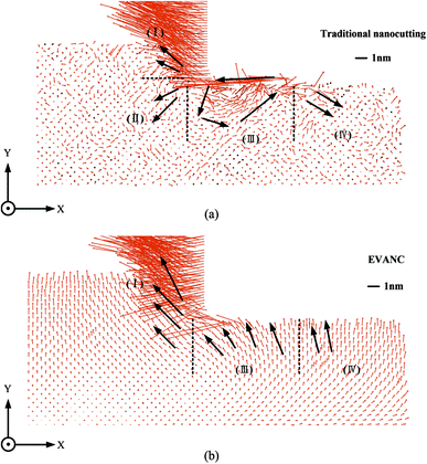 |
| | Fig. 11 Cross-section views of the silicon atom flow field during the nanocutting process. (a) Traditional nanocutting; (b) elliptical vibration-assisted nanocutting. | |
Fig. 11(b) is the atom flow field snapshot of EVANC. It is clear that there is a chip-forming region, cutting region, and finished region, but no compressive-induced region. The atoms in region (I) in Fig. 11(b) obliquely move upward to form the chips. The unanimous movement of silicon atoms results in a ductile deformation because there is no condition for crack formation. The stress state of atoms in region (I) is the same. The same situation occurs in regions (III) and (IV). The arrows for the atoms in these regions have similar motion states, suggesting that the stress state is similar. The ductile-mode cutting for this form leads to a better surface quality. Therefore, according to the atom flow field of the silicon atoms, EVANC has a positive effect on the silicon surface finish and the reduction of the affected silicon layer during the cutting process.
3.5. Analysis of the temperature via EVANC and traditional nanocutting
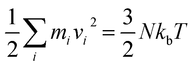
Fig. 12 gives the temperature contour for EVANC and traditional nanocutting. The temperature of the atoms during the simulations can be computed using the following conversion between the kinetic energy and temperature:| |
 | (15) |
where N is the number of atoms, vi represents the velocity of the i atom, kb is the Boltzmann constant (1.3806503 × 10⁻²³ J K−1), and T represents the atomistic temperature. However, the instantaneous fluctuation of the atomic kinetic energy is very high and thus the temperature is averaged in an area with a 1.5 nm cutoff radius to convert it into an equivalent temperature. The temperature in the chip zone cut by EVANC is above 2000 K, which is much higher than the traditional nanocutting induced chip zone. The temperature under the chip zone (circled by blue dotted line) with EVANC is also higher and ranges from 600 K to 1600 K, whereas the temperature in the traditional way ranges from 400 K to 800 K. This huge difference is because more kinetic energy has been exerted on the diamond tool and this energy transfers to the workpiece, which leads to a rise in the cutting temperature. The high temperature softens the cutting zone and may have a positive effect on the phase transformation and thereby makes EVANC easier.
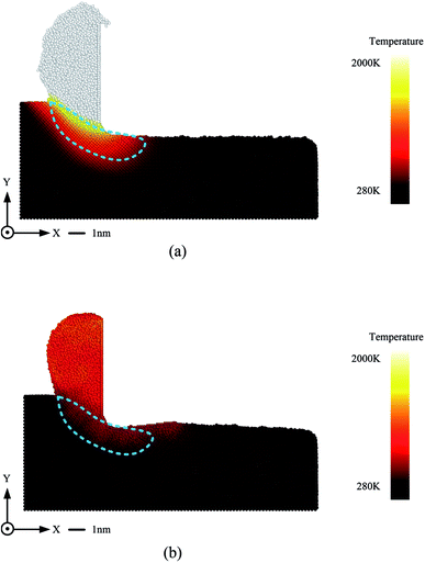 |
| | Fig. 12 Cross-section views of temperature contours during the nanocutting process. (a) Elliptical vibration-assisted nanocutting and (b) traditional nanocutting. | |
3.6. Analysis of the cutting force via EVANC and traditional nanocutting
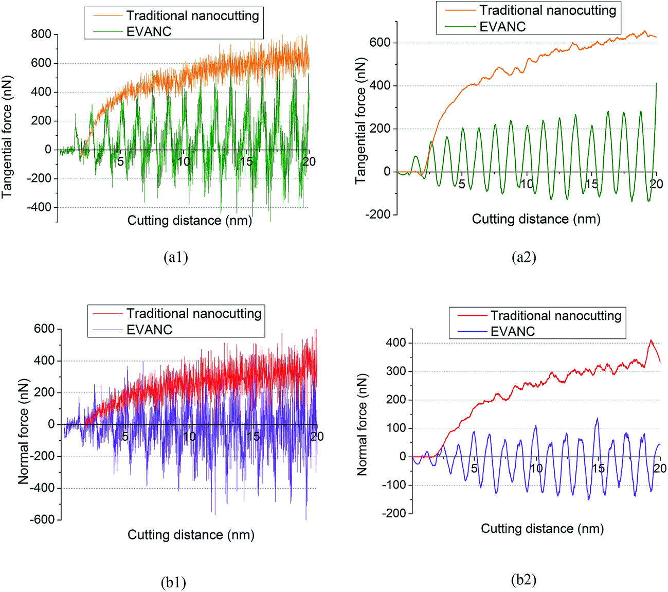
Forces in the MD simulations reflect the interaction between the diamond tool and the specimen. Fig. 13 presents the tangential force and normal force of traditional nanocutting and EVANC. Fig. 13(a1) and (b1) represent the original calculated curves of the tangential force and normal force. The calculated curves have been filtered, as shown in Fig. 13(a2) and (b2), to clarify the results.
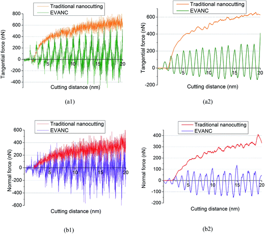 |
| | Fig. 13 Nanocutting force–displacement curves in MD simulations. (a1) Calculated curves of tangential force; (a2) filtered curves of tangential force. (b1) Calculated curves of normal force; (b2) filtered curves of normal force. | |
In the MD simulation process, carbon atoms at the bottom of the diamond tool and silicon atoms at the specimen surface adhere to each other. Therefore, the value of the tangential force and normal force during EVANC can sometimes be negative. In Fig. 13(a2), the tangential force in EVANC is lower than that of traditional nanocutting. As abovementioned, traditional nanocutting is the brittle-mode cutting; therefore, the tangential force is mainly generated from splitting the c-silicon structure. However, in EVANC, the tangential force originates from pressing the amorphous silicon structure to form chips. Destroying the bonds of silicon on the diamond structure is more difficult compared to removing amorphous silicon. Therefore, the tangential force of EVANC is smaller. Fig. 13(b2) shows that the normal force during EVANC is also lower than that of traditional nanocutting. This is because the residual stress under the cutting tool originating from EVANC is smaller and does not have a strong effect on the cutting tool. The smaller tangential force and normal force can reduce the friction between the workpiece and the cutting tool. This is beneficial for reducing the cutting energy and cutting heat, thereby reducing the tool wear and prolonging the tool life.
3.7. Discussion on the rationality of MD simulations with small cutting depth
Xiao et al.16 found cracks in their simulations. They concluded that the ductile-mode cutting can change into the brittle-mode cutting as the cutting depth increases in the traditional nanocutting. In ref. 15, further investigation on the traditional nanocutting was performed and it was discovered that the cutting depth, angle of the cutting tool rake face, and radius of the cutting tool can influence the ductile–brittle transition. Moreover, the radius of the cutting tool can also influence the ductile–brittle transition cutting depth. When the tool radius is small enough, the transition depth can also be smaller.
In experiments, cracks are easily observed using SEM and other microscopes, and the cracks can designate the brittle-mode cutting. However, in MD simulations, a crack is the result of the brittle-mode cutting, but not the reason. The signal for the brittle-mode cutting is that δyy in front of the cutting tool shows a tensile stress state, which is marked as the PEAK in the references (already observed in our study). The tensile stress leads to the different motion of atoms, as discussed in Section 3.4. The stress state and motion of the atoms explain the mechanism of the brittle-mode cutting of the traditional nanocutting on the atomic scale. When the cutting depth is larger, the tensile stress can be large enough and may lead to crack formation, which is consistent with the results reported by Xiao et al.16 The purpose of our research is to make comparisons between EVANC and traditional nanocutting and show that EVANC is different from the traditional nanocutting because there is a different mechanism.
4. Conclusion
Large-scale MD simulations have been performed in this study to investigate the surface quality and brittle–ductile transition during EVANC and traditional nanocutting. Conclusions are drawn based on the simulation results as follows:
(1) According to the atom arrangement during the nanocutting process, EVANC is a ductile-mode cutting on the silicon specimen. Traditional nanocutting shows a brittle cutting mode.
(2) Chips and the cutting-induced surface of the traditional nanocutting are likely to bring about β-silicon, whereas a small amount of β-silicon is found in EVANC. The affected layer of the EVANC-induced surface is thinner than that of the traditional nanocutting-induced surface. This illustrates that the surface quality induced through EVANC is better. Elliptical vibration-assisted nanocutting shows a larger material removal rate and there is a little atom elastic recovery on the basement.
(3) Elliptical vibration-assisted nanocutting leads to a better stress state in the cutting-induced silicon specimen surfaces. The result shows that the EVANC-induced surface has a thinner residual stress layer. The stress in the affected area in front of the cutting tool during EVANC is much smaller than that during the traditional cutting.
(4) The silicon atom flow field view reveals that the atomic motion shows a consistency during EVANC. This illustrates, based on the atom movement, that EVANC leads to ductile-mode cutting. In the traditional nanocutting, there is an evident shunt in the chip-forming region during the cutting process, which leads to crack formation, indicating that traditional cutting on silicon is a brittle-mode cutting.
(5) Temperature in the chip zone and cutting region is higher through EVANC as compared to that of the traditional nanocutting. The high temperature may soften the material and have a positive effect on the phase transformation. This may make material removal easier.
(6) The ductile-mode cutting of silicon via elliptical vibration-assisted nanocutting leads to a smaller tangential force and normal force as compared to the traditional nanocutting. The smaller tangential force leads to a smaller cutting energy and tool wear. The smaller normal force leads to a lower stress state and a thinner residual stress layer.
As a result, elliptical vibration-assisted nanocutting changes the brittle-mode cutting into the ductile-mode cutting. It has positive effects on the machinability and surface finish of the silicon material.
Acknowledgements
This research is funded by Special Projects for the Development of National Major Scientific Instruments and Equipments (Grant No. 2012YQ030075), the National Natural Science Funds for Excellent Young Scholar (Grant No. 51422503), the National Natural Science Foundation of China (Grant No. 51275198), and Fund Guiding on Strategic Adjustment of Jilin Provincial Economic Structure Project (Grant No. 2014Z045), Major project of Jilin Province Science and Technology development plan (20150203014GX), and the special fund project of Jilin provincial industrial innovation (2016C030).
References
- E. Shamoto and T. Moriwaki, CIRP Annals-Manufacturing Technology, 1994, 43, 35–38 CrossRef.
- Z. Liang, Y. Wu, X. Wang and W. Zhao, Int. J. Mach. Tool. Manufact., 2010, 50, 728–736 CrossRef.
- H. Kahn, M. Troyer and V. Prabhu, Ceram. Trans., 1997, 86, 119–124 Search PubMed.
- I. Zarudi and L. C. Zhang, J. Mater. Process. Technol., 1998, 84, 149–158 CrossRef.
- J. Zhang, T. Cui, C. Ge, Y. Sui and H. Yang, Int. J. Mach. Tool. Manufact., 2016, 106, 109–126 CrossRef.
- D. E. Brehl and T. a. Dow, Precis. Eng., 2008, 32, 153–172 CrossRef.
- Negishi, Nobuhiko, Elliptical vibration assisted machining with single crystal diamond tools.
- E. Shamoto and T. Moriwaki, CIRP Annals-Manufacturing Technology, 1999, 48, 441–444 CrossRef.
- D. E. Brehl and T. a. Dow, Proc. ASPE., 2007, 40, 150–156 Search PubMed.
- E. Uhlmann and G. Spur, CIRP Annals-Manufacturing Technology, 1998, 47, 249–252 CrossRef.
- N. Suzuki, A. Nakamura, E. Shamoto, K. Harada, M. Matsuo and M. Osada, MHS 2003-Proc. 2003 Int. Symp. Micromechatronics Hum. Sci., 2003, pp. 221–226 Search PubMed.
- J.-D. Kim and I.-H. Choi, Int. J. Adv. Manuf. Tech., 1998, 14, 2–6 CrossRef.
- J.-D. Kim and I.-H. Choi, J. Mater. Process. Technol., 1997, 68, 89–98 CrossRef.
- Z. Liang, X. Wang, Y. Wu, L. Xie, L. Jiao and W. Zhao, Int. J. Mach. Tool. Manufact., 2013, 71, 41–51 CrossRef.
- P. Zhang, H. Zhao, L. Zhang, C. Shi and H. Huang, J. Comput. Theor. Nanosci., 2014, 11, 291–296 CrossRef CAS.
- G. Xiao, S. To and G. Zhang, Int. J. Mach. Tool. Manufact., 2015, 88, 214–222 CrossRef.
- B. R. Lawn, A. G. Evans and D. B. Marshall, J. Am. Ceram. Soc., 1980, 63, 574–581 CrossRef CAS.
- F. Cardarelli, Materials Handbook, 2008, vol. 8 Search PubMed.
- Y. Yang, H. Zhao, L. Zhang, M. Shao, H. Liu and H. Huang, AIP Adv., 2013, 3, 102106 CrossRef.
- S. Plimpton, J. Comput. Phys., 1995, 117, 1–19 CrossRef CAS.
- W. Humphrey, A. Dalke and K. Schulten, J. Mol. Graphics, 1996, 14, 33–38 CrossRef CAS PubMed , NaN, 27–28.
- A. Stukowski, Modell. Simul. Mater. Sci. Eng., 2009, 18, 15012 CrossRef.
- J. Li, Modell. Simul. Mater. Sci. Eng., 2003, 11, 173–177 CrossRef.
- B. Zhu, H. Zhao, D. Zhao, P. Zhang, Y. Yang, L. Han and H. Kui, AIP Adv., 2016, 6, 35015 CrossRef.
- Z.-C. Lin and J.-C. Huang, J. Mater. Process. Technol., 2008, 201, 477–482 CrossRef CAS.
- J. Tersoff, Phys. Rev. Lett., 1986, 56, 632–635 CrossRef CAS PubMed.
- J. Tersoff, Phys. Rev. B: Condens. Matter Mater. Phys., 1988, 37, 6991–7000 CrossRef.
- J. Tersoff, Phys. Rev. B: Condens. Matter Mater. Phys., 1988, 38, 9902–9905 CrossRef CAS.
- F. Cleri, Phys. Rev. B: Condens. Matter Mater. Phys., 2001, 65, 1–6 CrossRef.
- H. Zhao, C. Shi, P. Zhang, L. Zhang, H. Huang and J. Yan, Appl. Surf. Sci., 2012, 259, 66–71 CrossRef CAS.
- M. a. Hopcroft, W. D. Nix and T. W. Kenny, J. Microelectromech. Syst., 2010, 19, 229–238 CrossRef CAS.
- J. H. L. Pang, Lead Free Solder Mech. Reliab., 2012, 9781461404, pp. 1–175 Search PubMed.
- S. Z. Chavoshi, S. Goel and X. Luo, Modell. Simul. Mater. Sci. Eng., 2016, 24, 15002 CrossRef.
|
| This journal is © The Royal Society of Chemistry 2017 |

 Open Access Article
 This Open Access Article is licensed under a Creative Commons Attribution-Non Commercial 3.0 Unported Licence
 *a,
Jian Guana,
Pengliang Houb,
Shunbo Wanga and
Long Qiana
*a,
Jian Guana,
Pengliang Houb,
Shunbo Wanga and
Long Qiana