
 Open Access Article
 This Open Access Article is licensed under a
 Creative Commons Attribution 3.0 Unported Licence
Nanocrystals of CuCr2S4−xSex chalcospinels with tunable magnetic properties†
Karthik
Ramasamy
*a,
Hunter
Sims
b,
Sahar
Keshavarz
c,
Nariman
Naghibolashrafi
c and
Arunava
Gupta
*c
aCenter for Integrated Nanotechnologies, Los Alamos National Laboratory, Albuquerque, NM-87185, USA. E-mail: kramasamy@lanl.gov
bGerman Research School for Simulation Sciences, Jülich, Germany-52425
cCenter for Materials for Information Technology, The University of Alabama, Tuscaloosa, AL-35487, USA. E-mail: agupta@mint.ua.edu
First published on 8th April 2016
Abstract
Ferromagnetic materials exhibiting large spin polarization at room temperature have been actively pursued in recent years for the development of next-generation spintronic devices. Chromium-based chalcospinels are the only ternary chalcogenide-containing magnetic materials with Curie temperatures above room temperature. However, the magnetic and electronic properties of chromium-based chalcospinels at the nanoscale level are not well understood. We have developed a facile colloidal method for the synthesis of CuCr2S4−xSex (0 ≤ x ≤ 4) nanocrystals over the entire composition range. Systematic changes in the lattice parameter and elemental composition confirm formation of CuCr2S4−xSex (0 ≤ x ≤ 4) nanocrystals. The dimensions of the nanocrystals, as determined from TEM images, vary from 12 ± 1.4 nm to 21 ± 1.4 nm. The Curie temperature (TC) shows a systematic increase with increasing selenium content. Saturation magnetization and coercivity values of CuCr2S4−xSex (0 ≤ x ≤ 4) nanocrystals at 5 K are found to steadily increase up to x = 3. Electronic structure calculations as a function of composition and size using density functional theory suggest ferromagnetic ordering over the entire composition range with partial spin polarization for the bulk materials. Furthermore, the calculations predict complete opening-up of a gap at the Fermi level in the minority spin channel at reduced dimensions to render them completely spin polarized, i.e., display half-metallic characteristics.
Introduction
Spin-based devices offer a significant advantage over charge-based ones because they are typically nonvolatile, requiring zero idle power.1,2 This promises significant energy savings over purely charge-based electronics, allowing device density to be increased beyond limits imposed by manipulating charge alone.3 Present-day spintronic devices primarily utilize the tunneling magnetoresistance (TMR) effect, which is based on tunnel junctions consisting of two ferromagnetic electrodes separated by an insulating tunneling layer with thickness of only a few nanometers.4 The performance of TMR and other spintronic devices depends critically on the degree of spin polarization (P) of the ferromagnetic electrodes. Of particular interest are the so-called half-metallic ferromagnets, which are completely spin polarized with P = 1.5–7 A half-metallic material is simultaneously an excellent metal for majority-spin electrons and an insulator for minority-spin electrons. Because of selective spin injection, half-metallic materials can in principle be used as an ideal spin injector and detector in spin-logic devices.8 In a magnetic tunnel junction with half-metallic electrodes, one would have the exciting prospect of switching between conducting and insulating states when the relative magnetization orientations of the two electrodes are altered. Nevertheless, it is necessary that such ferromagnetic materials exhibit high spin polarization at or above room temperature for practical applications. For this purpose, chromium-based chalcogenide spinels are an attractive class of material possessing a wide variety of electronic and magnetic properties.9–14 In these materials, depending on A-site substitution, ferro/ferrimagnetic ordering with insulating/semiconducting or metallic type transport properties can be realized.15 Electronic structure calculations predict high spin polarizations in a large number of chromium-based chalcospinel compounds, including some with complete half-metallic characteristics.16,17 Moreover, copper-containing chalcospinel ferromagnets such as CuCr2E4 (E = S, Se or Te) meet the high Curie temperature requirement. The Curie transition temperature (TC) of CuCr2S4, CuCr2Se4 and CuCr2Te4 in the bulk are 377, 430 and 360 K, respectively.18,19 Band structure calculations for these compounds indicate a large density of states at the Fermi energy (EF) in the majority spin channel as compared to the small density of states in the minority channel, suggesting metallic characteristics with a high degree of spin polarization.12,13,16,17The exceptional spin-dependent properties along with ferromagnetic ordering at room temperature in bulk CuCr2E4 (E = S, Se or Te) compounds are attractive for practical applications. However, exploitation of their properties in nanodimensional form remains largely unexplored because of the lack of suitable synthetic methodologies for producing phase-pure material. Appropriate choice of molecular precursors and capping agents are essential ingredients for phase-pure synthesis of these complex chalcospinels in the form of nanocrystals. With careful choice of precursors, we have recently developed synthetic methodologies for CuCr2E4, (E = S, Se or Te) nanocrystals.20–24 Motivated by the semiconductor-like transport properties reported for bulk CuCr2S4−xSex (0 ≤ x ≤ 4),25 herein we report the colloidal synthesis of nanocrystals of CuCr2S4−xSex (0 ≤ x ≤ 4) along with their detailed magnetic properties, complimented with electronic structure calculations. Our investigations reveal ferromagnetic ordering over the entire composition range, with a systematic increase in the superparamagnetic blocking and Curie temperatures with increasing Se content. Band structure calculations using density functional theory predict metallic characteristics in the bulk for all compositions, with a large difference in density of states in the majority and minority spin channels at the Fermi energy, suggesting high spin polarization. Furthermore, at reduced dimensions the calculations predict opening-up of a gap in minority spins at the Fermi level, rendering them closer to a true half-metallic system.
Experimental details
Methods
All chemicals were used as received and the solvents were dried over molecular sieves and purged with high purity argon for 30 minutes before use. 1-Dodecanethiol (1-DDT, 98.0%), diphenyldiselenide (DPDS, 98.0%) and copper chloride (CuCl, 99.5%) were received from Alfa Aesar; chromium chloride (CrCl3·6H2O, ≥ 99.0%), oleylamine (OLA, 80–90%) and octadecylamine (ODA, ≥ 99.0%) were obtained from Acros Organics. Analytical grade hexane and ethanol were obtained from Aldrich Chemical Co.Synthesis of CuCr2S4−xSex (0 ≤ x ≤ 4) nanocrystals
Experiments were carried out in a fume hood under N2 atmosphere using a standard Schlenk line technique. For the synthesis of CuCr2S4−xSex nanocrystals, CuCl (0.25 mmol), CrCl3·6H2O (0.50 mmol) and ODA (10 gm) were degassed at room temperature for 30 min and put back under N2. This process was repeated three times and subsequently the reaction vessel was initially heated to 175–180 °C under vacuum followed by heating to 360–365 °C under nitrogen. Meanwhile, in a separate vessel a requisite amount of DPDS for achieving the desired mixed anion stoichiometry was dissolved in 2 mL of 1-DDT. This solution was then quickly introduced into the vessel containing the solution of metal salts when it reached 360 °C. The reaction vessel cooled down during the injection process and was quickly reheated to 360 °C and maintained at this temperature for 1 h for the reaction to proceed. The mix was then cooled down to 65–70 °C and a mixture of hexane (10 mL) and ethanol (15 mL) was added to precipitate the product. The black precipitate was isolated via centrifugation. The precipitate was dispersed in hexane and reprecipitated by addition of ethanol. The above described method was also followed for the synthesis of CuCr2Se4 nanocrystal, but using an excess of diphenyldiselenide in OLA.Characterization and measurements
Transmission electron microscopy (TEM) analysis was performed using a FEI-Tecnai, 200 kV transmission electron microscope equipped with a CCD camera for STEM, HAADF detector, and EDX. TEM image non-linear processing was carried out using Gatan digital micrograph version 3.4. Powder X-ray diffraction (XRD) patterns were recorded on a Rigaku Smart Lab II instrument equipped with Cu Kα radiation source operated at 40 kV and 44 mA. PDXL v2.0 software package from Rigaku was used to process the powder XRD data. Scanning electron microscope (SEM) imaging and EDX mapping analysis were carried out using a JEOL 7000 FE SEM equipped with energy dispersive X-ray spectroscopy (EDX), wavelength dispersive X-ray spectroscopy (WDS), electron backscatter diffraction (EBSD), secondary electron (SE), backscattered electron (BE) and transmission electron (TE) detectors. Scanning transmission electron microscopy (STEM) high-angle annular dark field imaging and EDX elemental mapping were performed using a FEI Company Titan G2 80–200 TEM/STEM operated at 200 kV and equipped with the X-FEG (an ultra-stable high-brightness Schottky FEG source), Super-X EDX detector system (4 windowless silicon drift detectors with a combined solid angle of 0.7 sr) and a spherical aberration corrector (CEOS DCOR) on the probe-forming optics. TEM image non-linear processing – Fourier filtering – was carried out using Gatan Digital Micrograph version 3.4. The Diamond 3.2k crystal viewer software was used to produce the simulated XRD patterns for all the NC compositions. Additionally, Rietveld refinement was performed using Match! software to match the experimental XRD patterns for the end members. Magnetic measurements were performed using a Quantum Design Dynacool Vibrating Sample Magnetometer (VSM) with MultiVu application.Band structure calculations
The electronic structures of CuCr2S4−xSex (0 ≤ x ≤ 4) were calculated within the PBE generalized gradient approximation26 to density functional theory, using the rotationally invariant “+U” formalism of Liechtenstein et al.27 All calculations were performed using the VASP28–31 code using PAW32 pseudopotentials generated by Kresse and Joubert33 and a plane-wave cutoff of 368.6 eV. In the bulk calculations, we used the primitive 14-atom unit cell of the Fd![[3 with combining macron]](https://www.rsc.org/images/entities/char_0033_0304.gif) m spinel lattice with a 16 × 16 × 16 Γ-centered k-point mesh integrated using the tetrahedron method with Blöchl corrections. The computed nanostructures were constructed using the full 56-atom cubic cell with 15 Å of vacuum on all sides. Our PBE+U calculations are conducted using the fully local double-counting correction with U = 3.4 eV and J = 0.9 eV for the Cr 3d orbitals. For CuCr2S4, we use a PBE+U-relaxed structure with a = 9.81 Å and the internal parameter u = 0.258. The PBE+U relaxed lattice parameters for CuCr2Se4 were a = 10.31 Å and u = 0.255, with intermediate a and differing u values for the mixed phases. We did not find significant effects arising from the specific configuration of S and Se ions at a given stoichiometry.
m spinel lattice with a 16 × 16 × 16 Γ-centered k-point mesh integrated using the tetrahedron method with Blöchl corrections. The computed nanostructures were constructed using the full 56-atom cubic cell with 15 Å of vacuum on all sides. Our PBE+U calculations are conducted using the fully local double-counting correction with U = 3.4 eV and J = 0.9 eV for the Cr 3d orbitals. For CuCr2S4, we use a PBE+U-relaxed structure with a = 9.81 Å and the internal parameter u = 0.258. The PBE+U relaxed lattice parameters for CuCr2Se4 were a = 10.31 Å and u = 0.255, with intermediate a and differing u values for the mixed phases. We did not find significant effects arising from the specific configuration of S and Se ions at a given stoichiometry.
Results and discussion
Phase-pure synthesis of CuCr2S4−xSex (0 ≤ x ≤ 4) nanocrystals is non-trivial, as it requires a delicate balance of reaction conditions. Copper and chromium ions are known to exist in variable oxidation states and thereby different stoichiometry binary chalcogenides can be readily formed. Moreover, copper ions readily react with chalcogenide donating agents to form copper chalcogenide nanocrystals, but chromium is relatively inert and requires extreme conditions for reaction. For the successful synthesis of CuCr2S4−xSex (0 ≤ x ≤ 4) nanocrystals, we developed a colloidal hot-injection method. In this synthesis method, we inject a mixture of DPDS and 1-DDT into a reaction vessel containing copper and chromium precursors along with octadecylamine as capping ligand at a fairly high temperature (360–365 °C). DPDS and 1-DDT function as selenium and sulfonating agents, respectively. We previously reported on the phase-pure synthesis of chromium-based sulfospinel nanocrystals and found that it is essential to use 1-DDT as a sulfonating agent, otherwise only the binary sulfides of copper and chromium are obtained.20 Similarly, it is important to use an appropriate selenium precursor for the synthesis of CuCr2S4−xSex (0 ≤ x ≤ 4) nanocrystals, particularly one that is miscible with the other precursors and also avoids formation of binary copper/chromium selenides and CuCr2Se4 nanocrystals. Considering these factors, we investigated several commonly used selenium donating agents, including trioctylphosphine selenium (TOP-Se), selenium in octadecene (ODE-Se), and diphenyldiselenide. Among them, only diphenyldiselenide is found to produce phase-pure CuCr2S4−xSex (0 ≤ x ≤ 4) nanocrystals. Injection of a mixture of diphenyldiselenide and 1-dodecanethiol into the high temperature reaction mix likely produce selenolate and thiolate ions, which then form coordination complex(es) with copper and/or chromium ions. Further heating of these in situ formed complexes generate the reactive nuclei needed for the formation and growth of the nanocrystals. It is noteworthy that the reactions have to be carried out at 360–365 °C, which is unusually high for the solution-phase synthesis of chalcogen-containing nanocrystals. Reactions at lower reaction temperatures (<350 °C) yield a mixture of the chalcospinel and non-magnetic CuCrS2/CuCrSe2 phases.We characterized the nanocrystals using powder X-ray diffraction to confirm their phase purity, crystallinity and mixed anion compositions. X-ray diffraction patterns in Fig. 1(a) show distinct diffraction peaks corresponding primarily to the (311), (222), (400), (511) and (440) planes of the cubic phase spinel compounds. The peaks positions for CuCr2S4 and CuCr2Se4 nanocrystals are in accordance with the standard diffraction patterns (ICDD: 21-0287 and 81-1986). A systematic shift in the diffraction peak positions to lower angles is observed with increasing selenium content, indicating lattice expansion due to formation of CuCr2S4−xSex (0 ≤ x ≤ 4) solid solution. A steady enhancement of the (222) peak intensity is also noted with increasing selenium content. The diffraction peaks for all the patterns can be indexed to phase-pure chalcospinel compositions, with absence of any binary sulfide/selenide and ternary CuCrS2/CuCrSe2 impurity phases (Fig. S1, ESI†). The lattice parameter (a) values estimated from Rietveld simulation (Fig. 1(d) and (e)), of the diffraction patterns are 9.947 ± 0.016 Å for x = 0 and 10.377 ± 0.012 Å for x = 4 (Table 1). It can be noted that the estimated lattice parameter for CuCr2S4−xSex (x = 4) is somewhat higher that of literature values (10.357 Å: ICDD: 03-065-4391). Crystal defects such as dislocation defects are known to expand the crystalline lattice. From TEM images in Fig. 2 and 3(d) it can be seen that the nanocrystals do have imperfections and the detailed analysis to understand the type of crystalline defects demands extensive microscopic investigation, which is beyond the scope of this manuscript. Vegard's plot of the lattice parameter shows a linear trend in lattice expansion with increasing selenium content, as seen in Fig. 1(c). The elemental composition of the nanocrystals has been determined using SEM-EDX on a large number of particles. Within the accuracy of the measurements (±5%), the ratio of Cu, Cr, S and Se for the different compositions are found to be close to the expected values. The elemental compositions are provided in Table 1. The representative SEM-EDX spectrum for CuCr2S4−xSex (x = 2) nanocrystals is given in Fig. 2(a), which clearly indicates the presence of Cu, Cr, S and Se. Further, the distribution of each element in the individual nanocrystals (x = 0–4) has been analyzed using TEM-EDX elemental mapping and it confirms uniform distribution of the elements (Fig. S2, ESI† for x = 3). In addition we have carried out EDX analysis on individual particles with different sizes and did not observe any appreciable variation in the elemental compositions (Fig. S3 and Table S1, ESI† for x = 3).
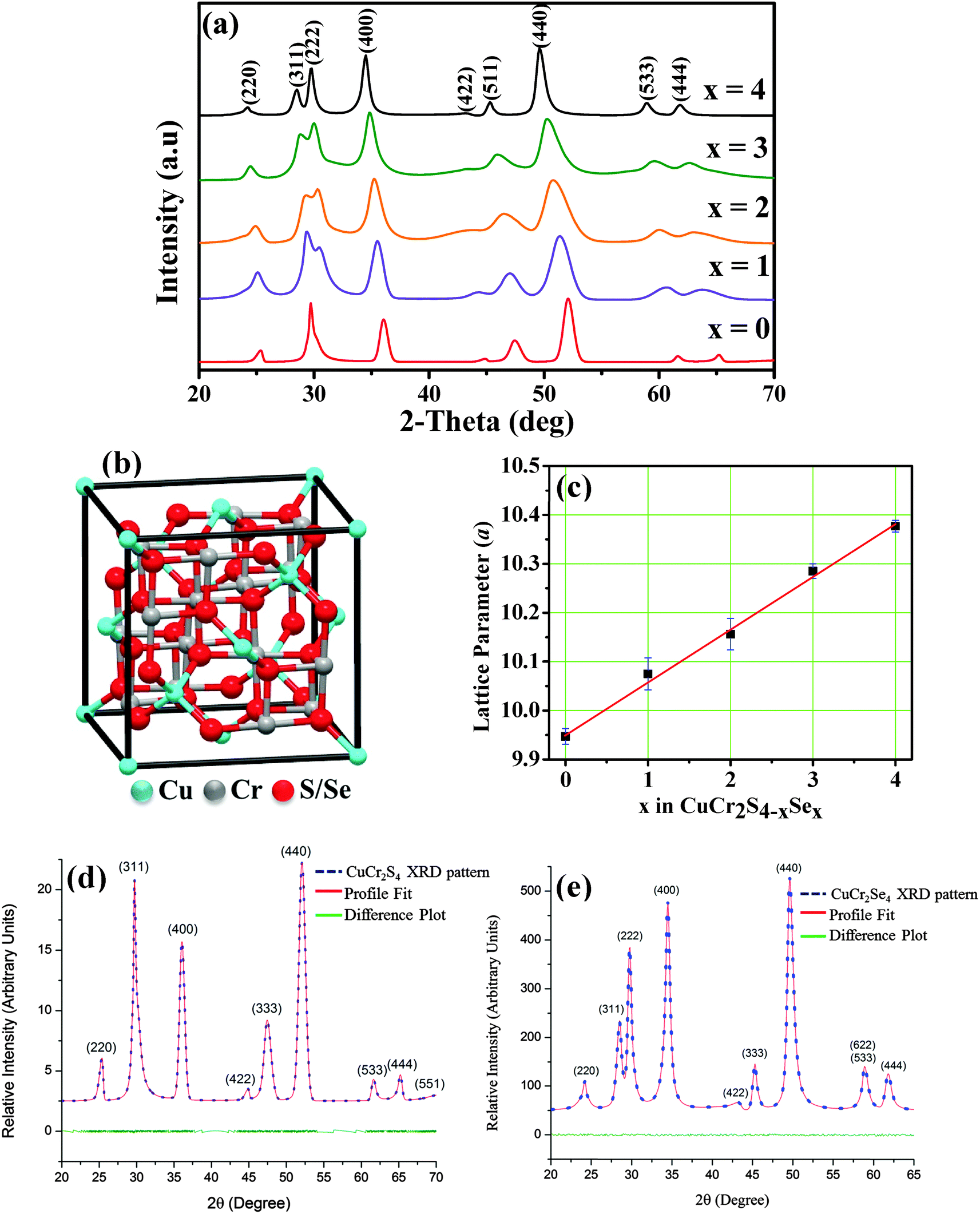 | ||
| Fig. 1 (a) XRD patterns of CuCr2S4−xSex (0 ≤ x ≤ 4) nanocrystals, (b) crystal structure of CuCr2S/Se4, (c) Vegard's plot. (d) and (e) Rietveld refinements showing good match with the experimental XRD data for CuCr2S4 and CuCr2Se4 nanocrystals. | ||
| CuCr2S4−xSex nanocrystals (x) | SEM-EDX data (% at.) Cu![[thin space (1/6-em)]](https://www.rsc.org/images/entities/char_2009.gif) :Cr:Se:S :Cr:Se:S |
Lattice constant (a) (Å) | Ave. particle size (TEM) (nm) | Ave. crystallite size (XRD) (nm) |
|---|---|---|---|---|
| 0 | 12.8:28.1:0.0:59.1 |
9.947 ± 0.016 | 21.0 ± 2.4 | 11.0 ± 0.8 |
| 1 | 12.6:29.2:13.9:44.3 |
10.075 ± 0.033 | 14.6 ± 3.0 | 7.0 ± 1.2 |
| 2 | 11.2:28.3:29.7:30.8 |
10.156 ± 0.032 | 16.0 ± 2.8 | 6.6 ± 0.7 |
| 3 | 11.3:26.7:40.8:21.2 |
10.285 ± 0.015 | 15.6 ± 2.5 | 8.5 ± 0.6 |
| 4 | 13.2:28.3:58.5:0.0 |
10.377 ± 0.012 | 12.0 ± 1.4 | 9.0 ± 0.6 |
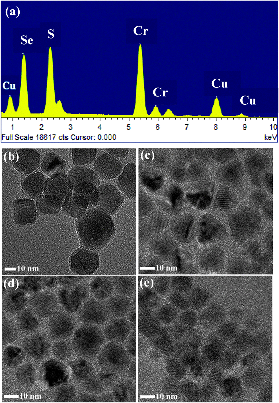 | ||
| Fig. 2 (a) EDX spectrum of CuCr2S4−xSex (x = 2) nanocrystals. TEM images of CuCr2S4−xSex nanocrystals (b) x = 0, (c) x = 1, (d) x = 2, and (e) x = 4. | ||
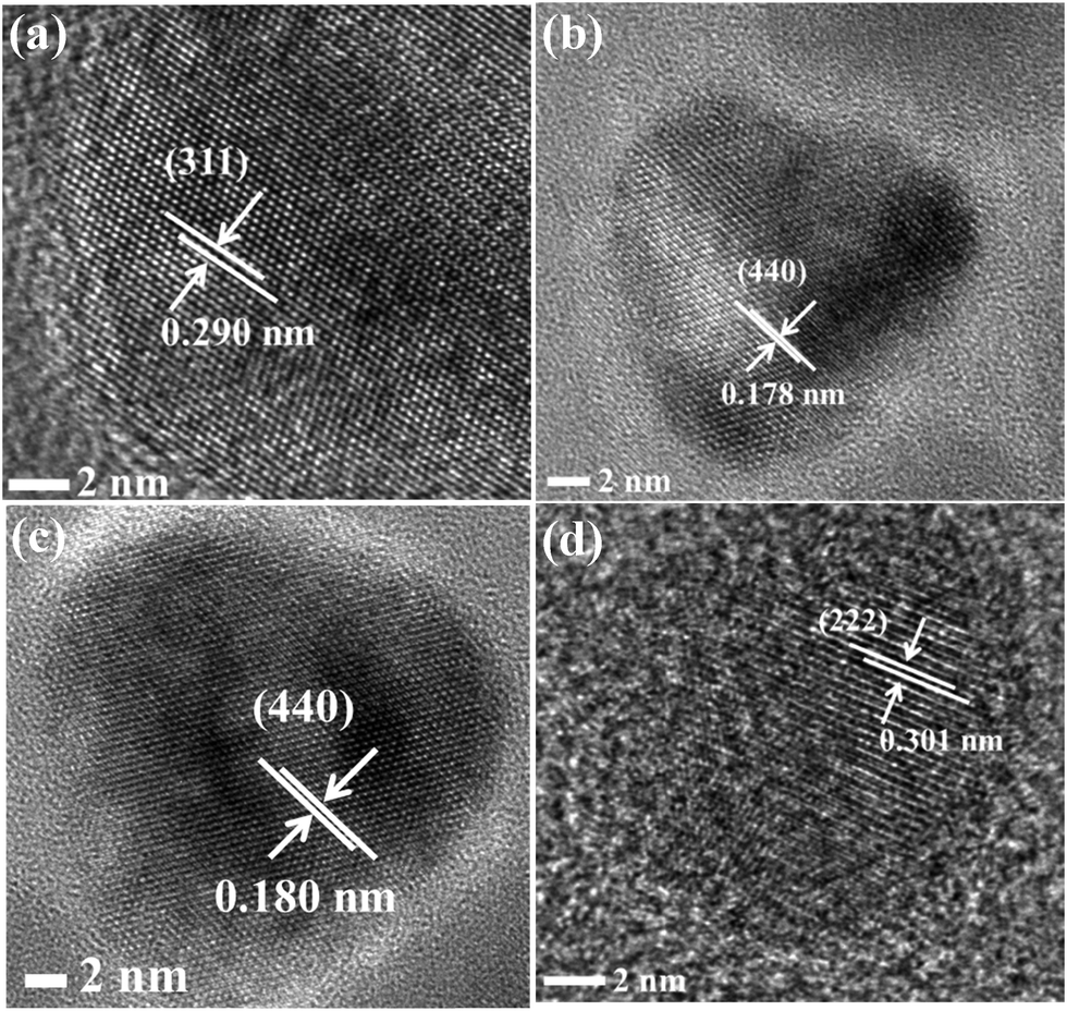 | ||
| Fig. 3 HRTEM images of CuCr2S4−xSex nanocrystals (a) x = 0, (b) x = 1, (c) x = 2, and (d) x = 4. | ||
We obtained shape and size information on the CuCr2S4−xSex (0 ≤ x ≤ 4) nanocrystals from transmission electron microscope images. TEM images of the nanocrystals are shown in Fig. 2(b)–(e). Cube-like nanocrystals of the end members CuCr2S4 and CuCr2Se4 are observed, while irregular to nearly pyramid-shaped nanocrystals are seen for the mixed CuCr2S4−xSex (1 < x < 3) compositions. The lateral dimensions of the nanocrystals, as estimated from the average of a large number of particles, are 21.0 ± 2.4 nm for x = 0, 14.6 ± 3 nm for x = 1, 16.0 ± 2.8 nm for x = 2, 15.6 ± 2.5 nm for x = 3, and 12 ± 1.4 nm for x = 4. These particles sizes are larger than the crystallite sizes estimated from powder X-ray diffraction (Table 1), suggesting that the individual nanocrystals may not be entirely single crystalline. High resolution transmission electron microscope (HRTEM) images of the nanocrystals are shown in Fig. 3(a)–(d). These images indicate that the nanocrystals are highly crystalline and exhibit well-defined lattice fringes. The distance between crystalline fringes for CuCr2S4 nanocrystals is measured to be 0.29 nm, corresponding to the (311) planes of cubic spinel. While the lattice fringe distances for CuCr2S4−xSex (1 < x < 3) nanocrystals are between 0.178 nm and 0.182 nm for the (440) planes, indicating a systematic lattice expansion on substitution of sulfur with selenium. The CuCr2Se4 nanocrystals exhibit (222) crystal planes that are separated by 0.301 nm. It is interesting to note that the morphology of CuCr2S4−xSex (1 < x < 3) nanocrystals is different from that of the end members, which is also reflected in the crystalline lattice fringe distances as a consequence of different growth directions.
In order to investigate the magnetic properties of the nanocrystals such as saturation magnetization, superparamagnetic blocking temperature, and Curie temperature, we have carried out measurements using a variable temperature vibrating sample magnetometer (VSM). The effect of selenium substitution on the saturation magnetization and coercivity has been analyzed by measuring the magnetization (M) as a function of applied magnetic field (H) at 5 and 300 K. The M–H curves at 300 K for different composition CuCr2S4−xSex (0 ≤ x ≤ 4) nanocrystals display superparamagnetic behavior with distinct “S” shape curves for the higher selenium content nanocrystals, as seen in Fig. S4 (ESI†). However, measurements at 5 K (Fig. 4(a)) indicate ferromagnetic behavior for all compositions, with coercivity values ranging between 250 and 550 Oe, signifying soft-ferromagnetic characteristics (Fig. 4(b)). Additionally, the loops exhibit magnetization saturation at field values around 2 Tesla for all samples except for the CuCr2S4 nanocrystals. The latter being in agreement with our previous observation.20,34 The magnetization measured at 2 Tesla increases systematically from 32.0 emu g−1 for x = 0 to 37.6 emu g−1 for x = 3, followed by an unexpected drop in value for pure CuCr2Se4 nanocrystals. The magnetization for CuCr2S4 nanocrystals is close to what we have reported earlier.20 However, the value for CuCr2Se4 nanocrystals is significantly lower than what we obtained for such nanocrystals synthesized using a different method. Notably, the average size of CuCr2Se4 nanocrystals is substantially smaller than the mixed composition nanocrystals.24,35 Materials at reduced dimensions can have more number of atoms at the surface than in the core, with the surface atoms having uncompensated dangling bonds due to inadequate passivation. The dangling bond spins are likely to couple antiferromagnetically with spins of the core atoms, leading to a reduced magnetization. Moreover, twin boundaries and point defects at cation and anion sites can contribute towards diluting the number of spins.
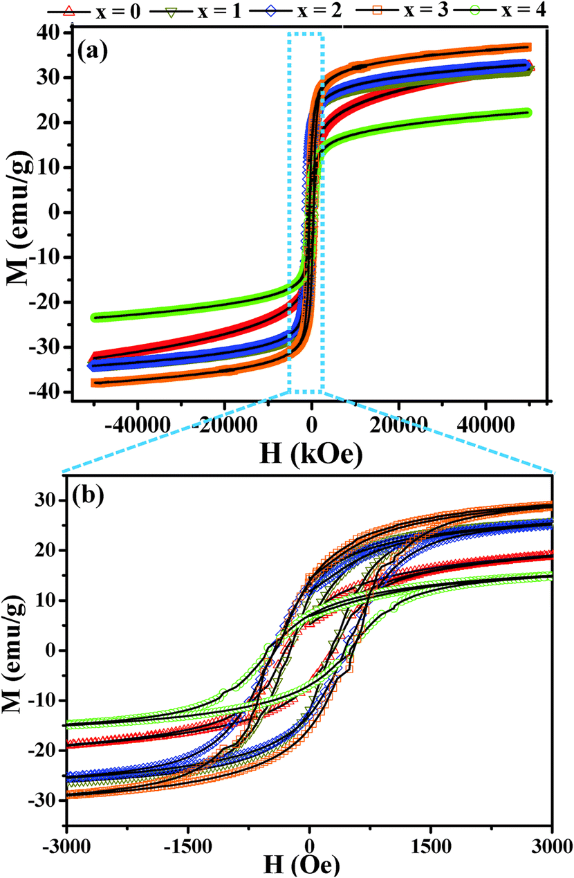 | ||
| Fig. 4 (a) Magnetization (M) versus magnetic field (H) measurements on CuCr2S4−xSex (0 ≤ x ≤ 4) nanocrystals at 5 K. (b) Expanded M–H loops measured at 5 K. | ||
For determining the superparamagnetic blocking temperature of the different composition nanocrystals, we have performed field-cooled (FC) and zero-field-cooled (ZFC) measurements at different applied fields between 50 and 1000 Oe. In ZFC measurements, the spins are frozen in random orientations at a low temperature and by increasing the temperature in the presence of an applied field the spins are aligned along the field direction. However, at higher temperatures the thermal energy competes by aiding in flipping the spin direction. The temperature at which the spin disorientation occurs is referred to as the blocking temperature (TB). The blocking temperature is determined by the magnetic anisotropy and volume of the material. From the coercivity values it can be noted that CuCr2S4−xSex (0 ≤ x ≤ 4) nanocrystals have low anisotropy and therefore their size has a significant influence on the blocking temperature. The ZFC curves are observed to be qualitatively similar for all the CuCr2S4−xSex (0 ≤ x ≤ 4) nanocrystals. Representative FC–ZFC plots for CuCr2S4−xSex (x = 3) nanocrystals are given in Fig. 5(a). In ZFC curve at 50 Oe field, a broad feature centered around 170 K can be observed, which is lower than the bifurcation temperature where the ZFC curve deviates from FC curve. With increasing applied field, the broad peak becomes more prominent and this peak along with the bifurcation point shift to lower temperatures. In an ideal case, nanocrystals with very narrow size dispersion show the peak and bifurcation point at the same temperature in FC–ZFC measurements, corresponding to the superparamagnetic blocking temperature (TB). However, for our nanocrystals we observe the peak and bifurcation point at different temperatures, suggesting a fairly broad size distribution as confirmed from TEM images in Fig. 2. In this case, we can refer the peak to an ensemble average blocking temperature and the bifurcation point as the largest blocking temperature. Despite the size distribution, we observed a systematic shift in both temperatures to higher values with increasing selenium content in the nanocrystals. The largest nanocrystal blocking temperature for all compositions of CuCr2S4−xSex (0 ≤ x ≤ 4) nanocrystals at different applied field values is plotted in Fig. 5(b).
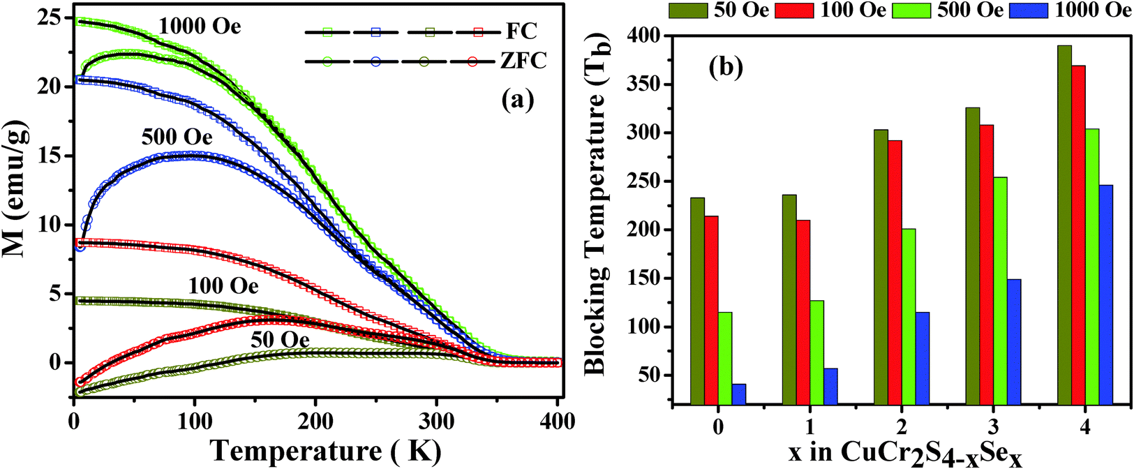 | ||
| Fig. 5 (a) Magnetization (M) as a function of temperature for field-cooled (FC) and zero-field-cooled (ZFC) measurements at 1000 Oe, 500 Oe, 100 Oe and 50 Oe for CuCr2S4−xSex (x = 3). (b) Graph showing comparison of superparamagnetic blocking temperature (TB) of CuCr2S4−xSex (0 ≤ x ≤ 4) at different measurement fields. | ||
Further, to study the effect of anion substitution on Curie transition temperature (TC) in the CuCr2S4−xSex (0 ≤ x ≤ 4) nanocrystals, we have carried out magnetization (M) versus temperature (T) measurements with an applied field of 2 Tesla. We observe an increase in the transition temperature with increasing selenium content (Fig. 6(a)). The temperature at which the magnetization value approaches zero are measured to be 340 K for x = 0; 320 K for x = 1; 350 K for x = 2; 370 K for x = 3 and over 400 K for x = 4 (Table 1). The values for CuCr2S4 and CuCr2Se4 nanocrystals are in agreement with our previous reported results and are somewhat lower than the bulk TC values.20,24,25,36 Moreover, the observed lowering of Curie temperature (320 K) for x = 1 and subsequent systematic increase of TC for higher selenium content samples is similar to the trend reported for bulk CuCr2S4−xSex (0 ≤ x ≤ 4).25 This behavior has been attributed to the existence of antiferron (disrupted ferromagnetic ordering) regions in the mixed chalcospinels.25 We have also carried out isothermal measurements of the magnetization versus applied magnetic field for more accurate determination of the transition temperatures. Representative isothermal plot for CuCr2S4−xSex (x = 2) is given in Fig. 6(b). Based on the isothermal measurements near the transition temperature, we have determined the TC for the different composition samples by using the Arrott plot method (isothermal plots of M2vs. H/M),37 as shown in Fig. 6(c). The Curie temperature determined using this method is in good agreement with those from M–T measurements.
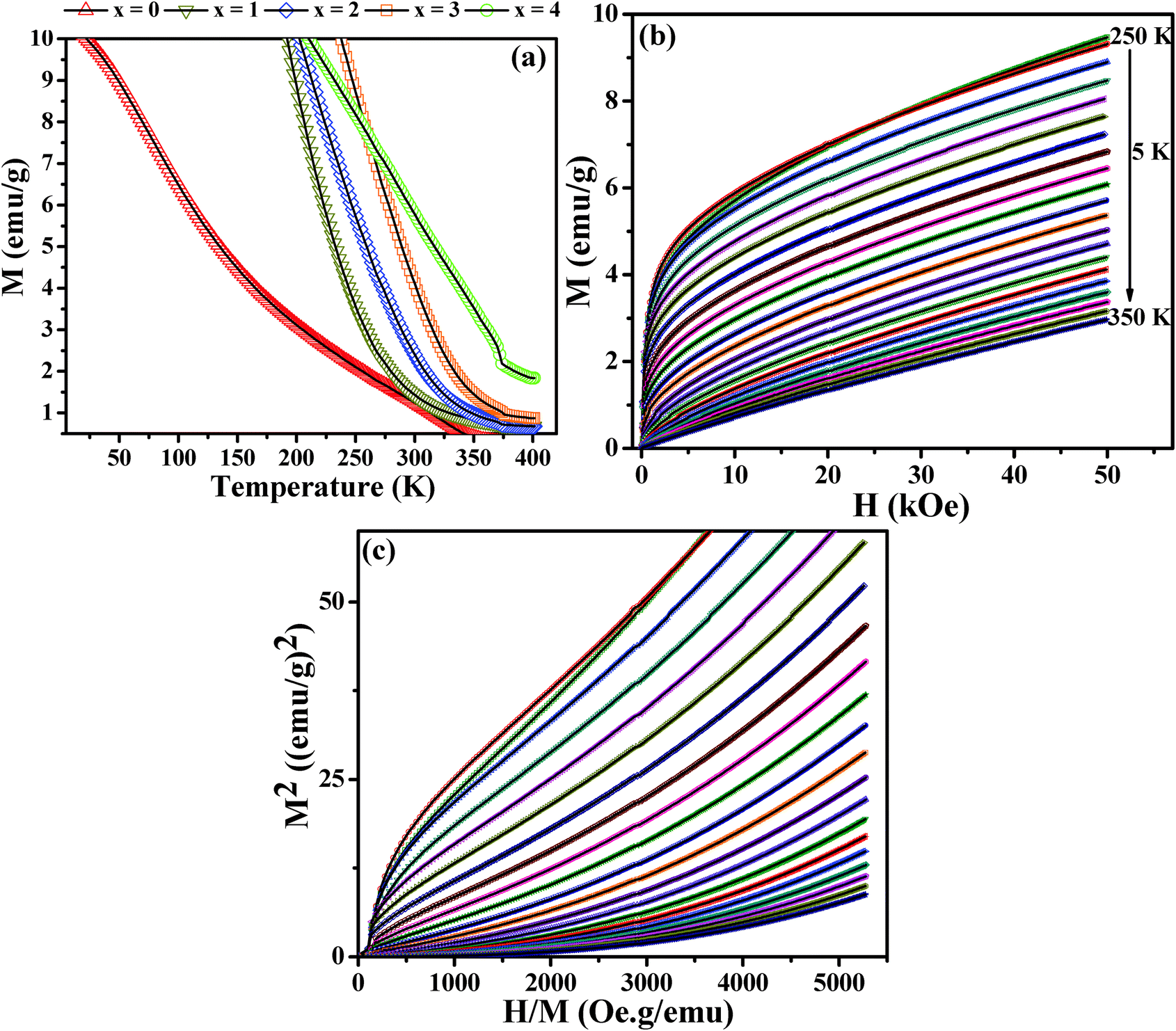 | ||
| Fig. 6 (a) Magnetization (M) versus temperature (T) measurements on CuCr2S4−xSex (0 ≤ x ≤ 4) nanocrystals with applied field of 20 kOe. Representative (b) isothermal and (c) Arrott plots for CuCr2S4−xSex (x = 2) nanocrystals. | ||
To help understand the variations in the magnetic properties with composition, we have carried out detailed band structure calculations both for the bulk and with reduced dimensions. We began by investigating the bulk properties of the CuCr2S4−xSex (0 ≤ x ≤ 4). We have previously published PBE+U calculations including CuCr2S4 as the end case for CoxCu1−xCr2S4.22 We will not discuss the x = 0 case in depth here but rather focus on how it differs from the substituted systems. Fig. 7 contains detailed views of the densities of states for the five systems in the vicinity of the Fermi level. Unsurprisingly, the plots are qualitatively quite similar due to the isovalent substitution, but we can observe several trends in the electronic structure as a function of Se content. We first consider the band gaps (always falling above the Fermi level, of course), noting that the majority and minority gaps both decrease with x but at different rates. The majority gap separates hybridized p–d states from the empty Cr eg states suggesting a charge transfer picture in which the size of the gap is primarily determined by an energy scale Δ that is related to the electronegativity of the anion (as given by the gap characterization picture of Zaanen, Sawatzky, and Allen38). Due to the empty minority Cr states, the energy difference between the occupied t2g and unoccupied eg states will be given mostly by the crystal field splitting rather than the intraorbital U. This description is borne out by the gap trend: the majority gap decreases steadily with x, falling to 50% of the CuCr2S4 value in CuCr2Se4.
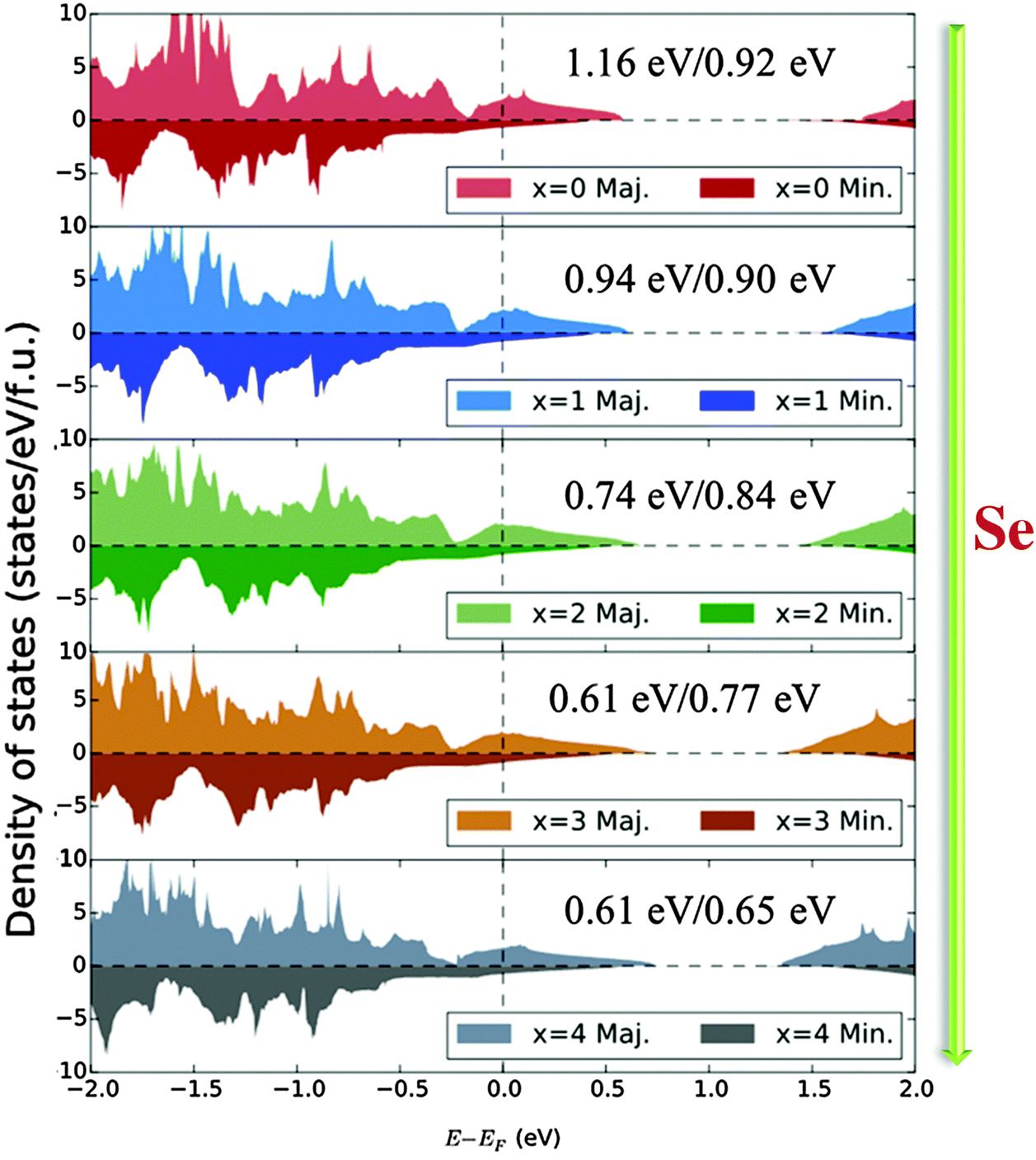 | ||
| Fig. 7 GGA+U densities of states for bulk CuCr2S4−xSex with x = 0 (top left) through x = 4 (bottom). The size of the gap (above the Fermi level) and the spin polarization decrease with x, while the minority “gap” becomes larger than that in the majority channel above x = 1. | ||
The minority valence band is dominated by the anionic p states, while the states above the gap are Cr d, whose position is determined both by U and the Hund's J (3.4 eV and 0.9 eV, respectively). This gap should be less affected by changes to the anion, and indeed the dependence of the size of the gap on x is weaker than in the majority channel, particularly for x ≤ 2. The difference in doping dependence (and in dependence on the strength of interactions in the B-site ion) gives one some control over not only the absolute but the relative size of the gaps: the minority gap becomes the larger one between x = 1 and x = 2. This potential for tunability has been noted in the theoretical band structures of CdCr2Te414 and the ferrites NiFe2O439 and CoFe2O4.40
Although the cell moment in our calculations follows the same trend as the magnetization in the nanocrystals – increasing through x = 3 and then dropping somewhat in CuCr2Se4, we find that the magnetization decreases monotonically with x from 100.6 emu g−1 at x = 0 to 63.4 emu g−1 at x = 4. We note that these are all much larger than the corresponding measurements, but as we discuss below, the computed magnetization does decrease in the finite systems.
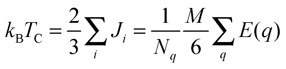
We have estimated the Curie temperature by comparing the energy of ferromagnetic and antiferromagnetic Cr magnetic orientations and computing TC within both the mean-field- (MFA) and random-phase-approximations (RPA). Intra-B-site antiferromagnetism is necessarily frustrated (spinels typically exhibit antiferromagnetic order between the tetrahedrally coordinated A sites and the octahedrally coordinated B sites when both are magnetic), so we have chosen a reasonable configuration as our AF case. TC is given by
 | (1) |
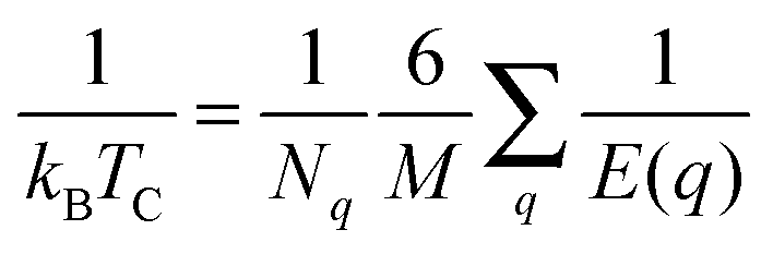 | (2) |
| CuCr2S4−xSex nanocrystals (x) | Saturation magnetization at 5 K emu g−1:emu mol−1:μB per Cr |
Coercivity Oe at 5 K | Curie temp. (TC) K | Calculated Curie temp. (TC) K | ||
|---|---|---|---|---|---|---|
| Nanocrystals | Bulk25 | MFA | RPA | |||
| 0 | 32.0:11503:0.43 |
300 | 340 | 377 | 606 | 404 |
| 1 | 33.0:9563:0.52 |
250 | 320 | 310 | — | |
| 2 | 33.6:13023:0.58 |
440 | 350 | 369 | 586 | 398 |
| 3 | 37.6:16287:0.73 |
440 | 370 | 392 | — | |
| 4 | 23.0:11012:0.49 |
540 | >400 | 437 | 656 | 450 |
We have also investigated fully confined nanostructures, considering 1 × 1 × 1 and 2 × 2 × 2 nanocrystals (hereafter referred to as 1 nm and 2 nm, respectively, roughly their length on each side) with 15 Å of vacuum on all sides. In order to better understand the size dependence of the electronic and magnetic properties, we have also considered 2 × 1 × 1 and 2 × 2 × 1 systems. It is not possible to achieve fully symmetrical surface termination while simultaneously maintaining stoichiometry and avoiding disorder in the interior of the nanocrystals – i.e. by only rearranging surface ions. For the 1 nm nanocrystals, we chose two terminations: one in which we did not alter the atomic positions from the bulk, yielding 3 Cu-terminated faces and 3 Cr–S/Se terminated faces, and one in which we attempted to symmetrize the surfaces as much as possible, yielding 4 opposing Cu-terminated faces and 2 opposing Cr–S/Se terminated faces (Fig. 8(a) and (b)). We also examined two terminations for the 2 nm nanocrystal: the same bulk-like-terminated structure from the 1 nm system and a fully Cu-terminated structure that is nearly but not entirely symmetrical (Fig. 8(c) and (d)). We find in general that the more symmetrical configurations are lower in energy by close to 200 meV per f.u.
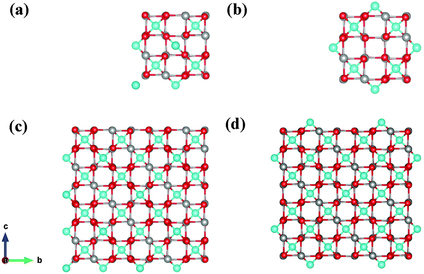 | ||
| Fig. 8 Clusters used to model 1 × 1 × 1 (a and b) and 2 × 2 × 2 (c and d) nanocrystals in our PBE+U calculations. We compared terminations based on the bulk structure (a and c) to those with more symmetrical Cu termination (b and d), finding the latter to be energetically favorable in all cases. | ||
We plot the density of states of the (symmetrically terminated) x = 0 confined systems in Fig. 9. As we discuss below, only the 1 nm system is a true half metal, with a band gap of about 1 eV in the minority channel; the majority valence band extends just beyond the Fermi level, yielding a highly spin-polarized metal. In all four systems, surface Cu 4s states join the Cr 3d states at the bottom of the minority conduction band in the symmetric cell and break free of the conduction band to form localized gap states in the unaltered-bulk-position cell. This is common at surfaces: electrostatic repulsion is reduced at the vacuum interface, reducing the cost of occupying these states. For the same reason, in the occupied anionic p states the energy levels associated with chalcogen sites with broken bonds reduce their energy with respect to those with the full complement. This is likely the cause of the enhanced spin polarization in the finite clusters. We note that the more pronounced peak structure of the 1 nm system is quickly smeared out as we increase the system size and approach the bulk, and there are no qualitative differences in the electronic structure of the 2 × 2 × 1 slab and the 2 × 2 × 2 cubic particles.
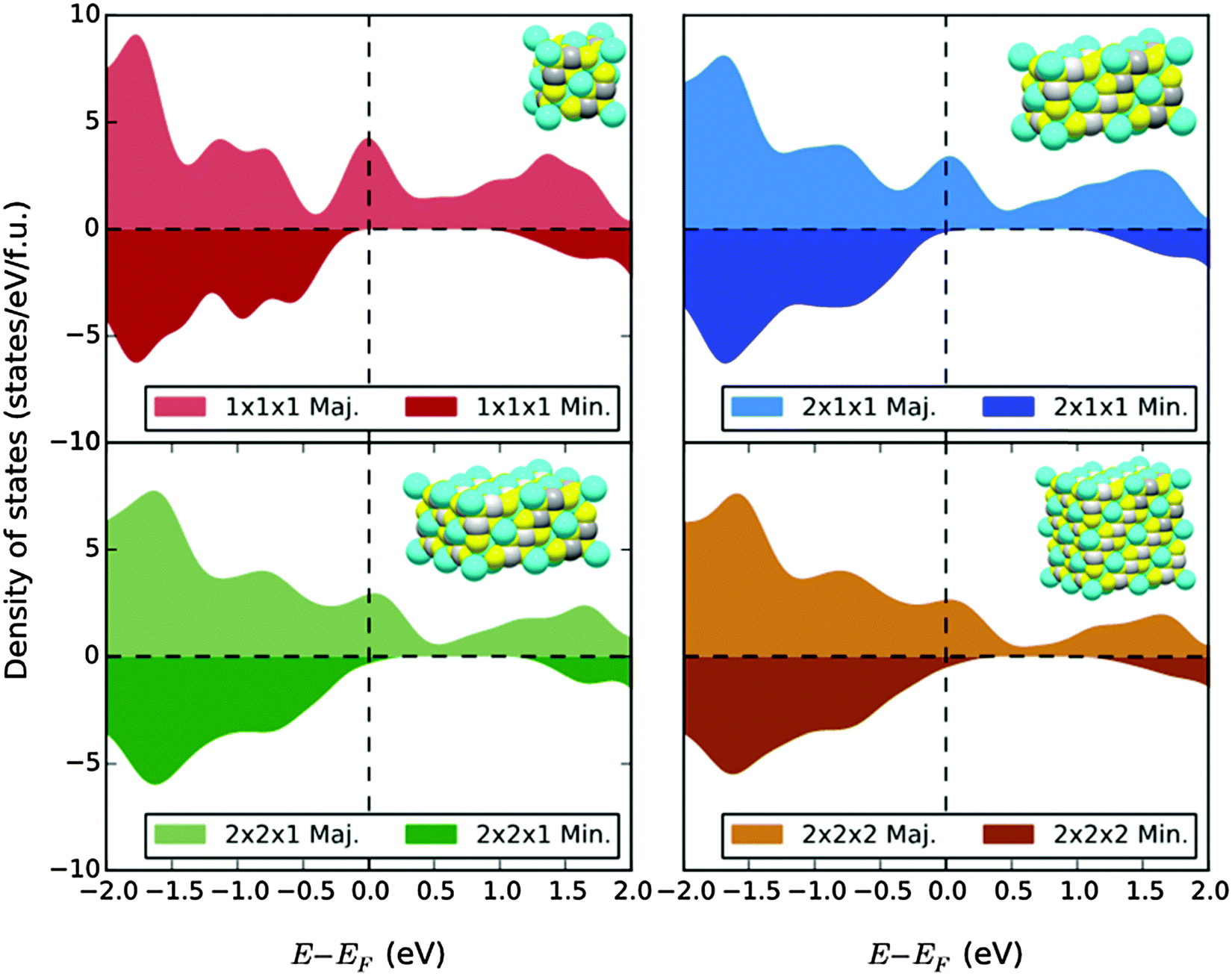 | ||
| Fig. 9 GGA+U densities of states for confined CuCr2S4 nanostructures composed of 56-atom cubic spinel unit cells. In all cases, the spin polarization is increased with respect to the bulk. The 1 × 1 × 1 nanostructure (top left) becomes fully half-metallic, but all larger “particles” retain some minority states at the Fermi level. The 2 × 2 × 2 system (bottom right) has nearly recovered the bulk electronic structure. (Inset: Crystal structures of CuCr2S4 in corresponding size). | ||
The magnetic moment of the confined systems scales with size: for x = 0, the 1 nm and 2 nm particles exhibit magnetizations of 86.2 emu g−1 and 94.1 emu g−1, respectively, the latter of which has already nearly recovered the bulk value. At x = 4, the magnetization of the 1 nm system is 58.1 emu g−1, a similar reduction. Here, the decreased magnetization does not arise from a partially nonmagnetic surface23 but primarily from enhanced opposing moments induced throughout the Cu and S/Se sites. We note that the more symmetrically terminated structures tend to have larger magnetizations.
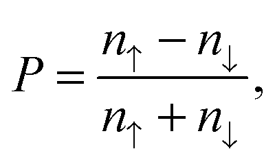
We can define the spin polarization P as
 | (3) |
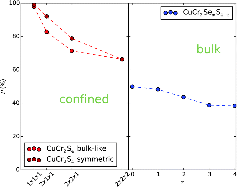 | ||
| Fig. 10 Spin polarization from GGA+U calculations for confined CuCr2S4 systems (as a function of number of cubic unit cells) and for bulk CuCr2S4−xSex (0 ≤ x ≤ 4) (as a function of x). The surface termination does not affect the polarization of the cubic particles. However, in the rod-like and slab-like structures symmetric termination (which is the lower in energy) increases the polarization by about 10%. In both cases, polarization decreases quickly with system size. | ||
Conclusion
Nanocrystals of CuCr2S4−xSex (0 ≤ x ≤ 4) have been synthesized over the entire composition using a mixture of 1-dodecanethiol and diphenyldiselenide as chalcogen agents and chlorides of copper and chromium as metal precursors. Systematic changes in the lattice parameter and elemental composition confirm formation of CuCr2S4−xSex (0 ≤ x ≤ 4) nanocrystals. Depending on selenium content, the nanocrystals vary in size from 12 ± 1.4 nm to 21 ± 1.4 nm. The magnetic transition temperature of the nanocrystals increases with increasing selenium content. Similarly, the saturation magnetization and coercivity values measured at 5 K are found to steadily increase up to x = 3. Band structure calculations using density functional theory suggest ferromagnetic ordering over the entire composition range with calculated magnetization values and Curie transitions temperatures trend consistent with the experimental results. The spin polarization calculated for bulk CuCr2S4−xSex (0 ≤ x ≤ 4) decreases from 50% to 38% with increasing selenium content. Interestingly, the calculation predicts a systematic increase in polarization value for the nanocrystals, with complete opening-up of a gap at the Fermi level in the minority spin channel at reduced dimensions.Acknowledgements
Synthesis, X-ray, TEM, SEM and magnetic characterization work was done at the University of Alabama, supported by the National Science Foundation under Grant No. CHE-1508259. Some TEM analysis was performed at the Center for Integrated Nanotechnologies, an Office of Science User Facility operated for the U.S. Department of Energy (DOE) Office of Science. Los Alamos National Laboratory, an affirmative action equal opportunity employer, is operated by Los Alamos National Security, LLC, for the National Nuclear Security Administration of the U.S. Department of Energy under contract DE-AC52-06NA25396.References
- S. A. Wolf, D. D. Awschalom, R. A. Buhrman, J. M. Daughton, S. von Molnár, M. L. Roukes, A. Y. Chtchelkanova and D. M. Treger, Science, 2001, 294, 1488–1495 CrossRef CAS PubMed.
- H. C. Koo, J. H. Kwon, J. Eom, J. Chang, S. H. Han and M. Johnson, Science, 2009, 325, 1515–1518 CrossRef CAS PubMed.
- I. Žutić, J. Fabian and S. Das Sarma, Rev. Mod. Phys., 2004, 76, 323–410 CrossRef.
- J. S. Moodera, L. R. Kinder, T. M. Wong and R. Meservey, Phys. Rev. Lett., 1995, 74, 3273–3276 CrossRef CAS PubMed.
- R. A. De Groot, F. M. Mueller, P. G. Van Engen and K. H. J. Buschow, Phys. Rev. Lett., 1983, 50, 2024–2027 CrossRef CAS.
- J. H. Park, E. Vescovo, H. J. Kim, C. Kwon, R. Ramesh and T. Venkatesan, Nature, 1998, 392, 794–796 CrossRef CAS.
- M. Jourdan, J. Minár, J. Braun, A. Kronenberg, S. Chadov, B. Balke, A. Gloskovskii, M. Kolbe, H. J. Elmers, G. Schönhense, H. Ebert, C. Felser and M. Kläui, Nat. Commun., 2014, 5, 3974 CAS.
- Y. Guo, F. R. Shen and X. Y. Chen, Appl. Phys. Lett., 2012, 101, 012410 CrossRef.
- C. P. Sun, C. L. Huang, C. C. Lin, J. L. Her, C. J. Ho, J. Y. Lin, H. Berger and H. D. Yang, Appl. Phys. Lett., 2010, 96, 2010–2012 Search PubMed.
- G. Catalan and J. F. Scott, Nature, 2007, 434, 364–367 Search PubMed.
- J. Bertinshaw, C. Ulrich, A. Günther, F. Schrettle, M. Wohlauer, S. Krohns, M. Reehuis, A. J. Studer, M. Avdeev, D. V. Quach, J. R. Groza, V. Tsurkan, A. Loidl and J. Deisenhofer, Sci. Rep., 2014, 4, 6079 CAS.
- M. Park, S. Kwon, S. Youn and B. Min, Phys. Rev. B: Condens. Matter Mater. Phys., 1999, 59, 10018–10024 CrossRef CAS.
- S. Bordács, I. Kézsmárki, K. Ohgushi and Y. Tokura, New J. Phys., 2010, 12, 053039 CrossRef.
- H. Sims, K. Ramasamy, W. H. Butler and A. Gupta, Appl. Phys. Lett., 2013, 103, 192402 CrossRef.
- K. G. Nikiforov, Prog. Cryst. Growth Charact. Mater., 1999, 39, 1–104 CrossRef CAS.
- Y. H. A. Wang, A. Gupta, M. Chshiev and W. H. Butler, Appl. Phys. Lett., 2008, 92, 173–176 Search PubMed.
- Y. H. A. Wang, A. Gupta, M. Chshiev and W. H. Butler, Appl. Phys. Lett., 2009, 94, 173–176 Search PubMed.
- P. K. Baltzer, H. W. Lehmann and M. Robbins, Phys. Rev. Lett., 1965, 15, 493 CrossRef CAS.
- J. B. Goodenough, Solid State Commun., 1967, 5, 577–580 CrossRef CAS.
- K. Ramasamy, D. Mazumdar, Z. Zhou, Y.-H. A. Wang and A. Gupta, J. Am. Chem. Soc., 2011, 133, 20716–20719 CrossRef CAS PubMed.
- K. Ramasamy, D. Mazumdar, R. D. Bennett and A. Gupta, Chem. Commun., 2012, 48, 5656–5658 RSC.
- K. Ramasamy, H. Sims, R. K. Gupta, D. Kumar, W. H. Butler and A. Gupta, Chem. Mater., 2013, 25, 4003–4009 CrossRef CAS.
- D. S. Negi, B. Loukya, K. Ramasamy, A. Gupta and R. Datta, Appl. Phys. Lett., 2015, 106, 182402 CrossRef.
- Y. H. A Wang, N. Bao, L. Shen, P. Padhan and A. Gupta, J. Am. Chem. Soc., 2007, 129, 12408–12409 CrossRef PubMed.
- L. I. Koroleva, J. Exp. Theor. Phys., 1994, 79, 153–162 Search PubMed.
- J. P. Perdew, K. Burke and M. Ernzerhof, Phys. Rev. Lett., 1996, 77, 3865 CrossRef CAS PubMed.
- A. I. Liechtenstein, V. I. Anisimov and J. Zaanen, Phys. Rev. B: Condens. Matter Mater. Phys., 1995, 52, R5467 CrossRef CAS.
- G. Kresse and J. Hafner, Phys. Rev. B: Condens. Matter Mater. Phys., 1993, 47, 558 CrossRef CAS.
- G. Kresse and J. Hafner, Phys. Rev. B: Condens. Matter Mater. Phys., 1994, 49, 14251 CrossRef CAS.
- G. Kresse and J. Furthmüller, Phys. Rev. B: Condens. Matter Mater. Phys., 1996, 54, 11169 CrossRef CAS.
- G. Kresse and J. Furthmüller, Comput. Mater. Sci., 1996, 6, 15 CrossRef CAS.
- P. E. Blöchl, Phys. Rev. B: Condens. Matter Mater. Phys., 1994, 50, 17953 CrossRef.
- G. Kresse and D. Joubert, Phys. Rev. B: Condens. Matter Mater. Phys., 1999, 59, 1758 CrossRef CAS.
- A. I. Pankrats, A. M. Vorotynov, V. I. Tugarinov, S. M. Zharkov, D. A. Velikanov, G. M. Abramova, G. M. Zeer, K. Ramasamy and A. Gupta, J. Appl. Phys., 2014, 116, 054302 CrossRef.
- C.-R. Lin, C.-L. Yeh, S.-Z. Lu, I. S. Lyubutin, S.-C. Wang and I. P. Suzdalev, Nanotechnology, 2010, 21, 235603 CrossRef PubMed.
- I. Nakatani, H. Nose and K. Masumoto, J. Phys. Chem. Solids, 1978, 39, 743–749 CrossRef CAS.
- R. L. Hadimani, Y. Melikhov, J. E. Snyder and D. C. Jiles, J. Magn. Magn. Mater., 2008, 320, 696–698 CrossRef.
- J. Zaanen, G. A. Sawatzky and J. W. Allen, Phys. Rev. Lett., 1985, 55, 418 CrossRef CAS PubMed.
- Q.-C. Sun, H. Sims, D. Mazumdar, J. X. Ma, B. S. Holinsworth, K. R. O'Neal, G. Kim, W. H. Butler, A. Gupta and J. L. Musfeldt, Phys. Rev. B: Condens. Matter Mater. Phys., 2012, 86, 205106 CrossRef.
- B. S. Holinsworth, D. Mazumdar, H. Sims, Q.-C. Sun, M. K. Yurtisigi, S. K. Sarker, A. Gupta, W. H. Butler and J. L. Musfeldt, Appl. Phys. Lett., 2013, 103, 082406 CrossRef.
Footnote |
| † Electronic supplementary information (ESI) available: Experimental and simulated XRD patterns for the different compositions, EDX elemental mapping, and M–H data at 300 K. See DOI: 10.1039/c5tc04448k |
| This journal is © The Royal Society of Chemistry 2016 |