
 Open Access Article
 This Open Access Article is licensed under a
 Creative Commons Attribution 3.0 Unported Licence
Poly(methyl methacrylate)-grafted ZnO nanocomposites with variable dielectric constants by UV light irradiation
Kenichi
Hayashida
*a and
Yasuhiro
Takatani
b
aMaterials and Processing Dept. II, Toyota Central R&D Labs., Inc., Nagakute, Aichi 480-1192, Japan. E-mail: e1440@mosk.tytlabs.co.jp
bMaterials Analysis and Evaluation Dept., Toyota Central R&D Labs., Inc., Nagakute, Aichi 480-1192, Japan
First published on 29th March 2016
Abstract
A series of poly(methyl methacrylate)-grafted ZnO nanoparticles (PMMA–ZnO) were synthesized using a surface-initiated polymerization technique and the optical and dielectric properties of PMMA–ZnO were studied. The dielectric constant εr′ of PMMA–ZnO thin films was highly increased by irradiation of UV light. It is indicated that electrons in the ZnO nanoparticles are excited from a valence band to a conductive band by absorption of UV light, resulting in a large increase in εr′ owing to Maxwell–Wagner polarization of the resultant free electrons. On the other hand, the dissipation factor (tan![[thin space (1/6-em)]](https://www.rsc.org/images/entities/char_2009.gif) δ) of PMMA–ZnO is very low and almost constant during UV irradiation because PMMA–ZnO is electrically insulated by the grafted PMMA chains on the ZnO nanoparticles. Also, it was confirmed that due to the grafted PMMA chains, PMMA–ZnO nanocomposites exhibited low light scattering in addition to strong absorption of UV light. The low light scattering of PMMA–ZnO would enhance the absorption efficiency of UV light and therefore contribute to the large increase in εr′ for PMMA–ZnO. Thus, PMMA–ZnO is a promising material for high sensitivity and low loss UV light sensors using the change in εr′.
δ) of PMMA–ZnO is very low and almost constant during UV irradiation because PMMA–ZnO is electrically insulated by the grafted PMMA chains on the ZnO nanoparticles. Also, it was confirmed that due to the grafted PMMA chains, PMMA–ZnO nanocomposites exhibited low light scattering in addition to strong absorption of UV light. The low light scattering of PMMA–ZnO would enhance the absorption efficiency of UV light and therefore contribute to the large increase in εr′ for PMMA–ZnO. Thus, PMMA–ZnO is a promising material for high sensitivity and low loss UV light sensors using the change in εr′.
Introduction
Dielectric materials are usually used to store electrical energy as capacitors.1 Among dielectric materials, polymer materials have the advantage of high flexibility, lightness, and processability although the very low dielectric constant εr′ of polymer materials (εr′ = 2–3) strongly impedes improvement of the capacitance C of capacitors. Because of the high εr′ of ceramic materials (εr′ > 100), polymer/ceramic composite materials have been much developed over the last few decades. BaTiO3, one of the ferroelectric metal oxides, has been most widely used for enhancement of εr′.2–10 On the other hand, for other dielectric applications such as variable capacitors, pressure sensors, and touch sensors, a change of C for these systems is important, and high εr′ is not always required.11–17 The distance between two electrodes d and/or the area of the electrodes S are varied by physical operations, changing the C for the systems: C = ε0εr′S/d, where ε0 is the permittivity of vacuum. Also, C for a system can be changed when the εr′ of a dielectric material is varied by a stimulus. For example, if the εr′ of a polymer material could be changed by irradiation of light, the polymer material can be used not only for a variable capacitor but also for a light sensor. However, no polymer material with a variable εr′ by light has been reported so far.Here, we suggest a composite system where semiconductor particles are incorporated in a polymer matrix. It is known that the conductivity of some semiconductors is strongly enhanced by absorption of light because electrons are excited from a valence band to a conductive band.18 Therefore, during light irradiation, the polymer/semiconductor composite should exhibit a high εr′ owing to Maxwell–Wagner polarization of the resultant free electrons.19 Unfortunately, it is expected that the dielectric loss of the composite simultaneously becomes very large owing to leak current by the free electrons. Generally, for polymer/inorganic particle composite systems, three-dimensional networks of inorganic particles are formed in the polymer matrix because interaction between the inorganic particles is stronger than that between the inorganic particles and the matrix polymer.9,20 For the polymer/semiconductor composite under light irradiation, therefore, the large leak current would be caused through the conductive networks of semiconductor particles. If the individual semiconductor particles are isolated and uniformly distributed in the polymer matrix, the composite should be electrically insulated to be a low-loss dielectric material. A successful method of insulation would be polymer grafting on the semiconductor particles. It has been reported that even carbon nanotubes with very high conductivity can be insulated by polymer grafting.21–23
In order to obtain a large εr′ change Δεr′ for the polymer/semiconductor composite, it is desirable that the intrinsic εr′ of the semiconductor is small enough in addition to high conductivity during light irradiation. The larger Δεr′ provides better sensitivity of the light sensor. Furthermore, in terms of absorption efficiency of light for the composite, the smaller diameter of the semiconductor particles is desirable because of low scattering of light by the particles. Based on the above, ZnO is one of the most promising candidates for semiconductors with a variable εr′. ZnO exhibits strong absorption of ultraviolet (UV) light,24,25 and the εr′ of pure ZnO is as low as about 10.26 In addition, a variety of ZnO nanoparticles are commercially and inexpensively available.24,25
In this study, poly(methyl methacrylate) (PMMA) was grafted on ZnO nanoparticles using a surface-initiated atom transfer radical polymerization (SI-ATRP) technique.27 The optical and dielectric properties of the PMMA-grafted ZnO nanocomposites (PMMA–ZnO) were compared to those of conventional nanocomposites prepared by blending PMMA with the initiator-modified ZnO nanoparticles (PMMA/ZnO). We demonstrated that PMMA–ZnO exhibits a large Δεr′ by irradiation of UV light with a low dissipation factor (tanδ). To the best of our knowledge, this is the first report on polymer/semiconductor composites with a variable εr′ by light irradiation although many studies have been reported on the dielectric properties of polymer/semiconductor composites such as polymer/ZnO composites.28–37
Experimental
Sample preparation
ZnO nanoparticles with an average diameter of 15 nm were obtained from Kanto Denka Kogyo (Japan). The density of the ZnO nanoparticles was determined to be 5.22 g cm−3 using an ultrapycnometer (UPY-2, Quantachrome). Procedures for modification of the ZnO nanoparticles were as follows (Fig. 1): | ||
| Fig. 1 Synthesis procedure of poly(methyl methacrylate)-grafted ZnO particles (PMMA–ZnO). (a) Preparation of ATRP initiator-modified ZnO particles (ZnO–Br). (b) Surface-initiated ATRP of methyl methacrylate using ZnO–Br. | ||
Amine-modification of the ZnO nanoparticles: trimethoxy[3-(methylamino)propyl]silane (840 μl, 4.3 mmol) was added to the ZnO nanoparticles (10 g) homogeneously dispersed in dimethylformamide (DMF) (97 ml) containing a small amount of water (0.5 ml). The dispersion was sonicated and kept at 50 °C for 6 h. The amine-modified ZnO nanoparticles (ZnO–NHMe) were purified by 3 cycles of centrifugation and redispersion in acetonitrile (AN).
Immobilization of ATRP initiators on the ZnO nanoparticles: p-(bromomethyl)benzyl 2-bromoisobutylate (BBnBiB)27 (1.0 g, 2.9 mmol) and 1,8-bis(dimethylamino)naphthalene (0.60 g, 2.8 mmol) were added to ZnO–NHMe (16 g) dispersed in AN (95 ml). The mixture was sonicated and kept at 40 °C for 12 h. The initiator-modified ZnO nanoparticles (ZnO–Br) were purified by 3 cycles of centrifugation and redispersion in DMF.
SI-ATRP from the ZnO nanoparticles: the following is an example. N,N-Dimethylacetamide (90 ml) was added to ZnO–Br (16.8 g) and CuBr (14.3 mg, 100 μmol) in a N2 atmosphere. After sonication of the mixture, 2,2′-bipyridyl (46.8 mg, 300 μmol) in methyl methacrylate (60 ml) was added, and the dispersion was kept at 60 °C for 2.5 h. The resultant core–shell nanoparticles (PMMA–ZnO) were precipitated in methanol and freeze-dried by 1,4-dioxane.
PMMA/ZnO nanocomposites were prepared by blending ZnO–Br with PMMA. First, ZnO–Br and the PMMA matrix were added to 1,4-dioxane and homogeneously dispersed by sonication. The dispersion was quickly frozen in liquid nitrogen, and then freeze-dried under vacuum. Subsequently, the preliminary mixed PMMA/ZnO nanocomposites were further kneaded in a molten state. Thus-obtained PMMA/ZnO and PMMA–ZnO nanocomposites were molded into disk-like specimens with a diameter of 33 mm and a thickness of ∼0.52 mm by compression at 120–140 °C.
Measurements
The ZnO contents in PMMA/ZnO and PMMA–ZnO were determined by thermogravimetry (TG). The sample taken in a platinum pan was heated from room temperature to 600 °C at a rate of 10 °C min−1 under an air flow (200 ml min−1) using a thermobalance (Thermo Plus TG 8120, Rigaku). The volume fraction of ZnO ΦZnO for PMMA/ZnO and PMMA–ZnO was calculated using a density of 5.22 g cm−3 for the ZnO nanoparticles (the residue after TG measurement) and of 1.19 g cm−3 for the organic components (the weight loss during the TG measurement).SEM images of the modified ZnO nanoparticles were obtained using an SEM (S-5500, Hitachi) operated at an accelerating voltage of 1 kV. The cross-section of the molded samples that had been flattened with the argon ion beam using a cross section polisher38 was observed at an accelerating voltage of 2 kV.
Transmission spectra of the disk-like specimens were obtained using a UV-vis spectrophotometer (UV-3600, Shimadzu), where the sample was scanned in the wavelength λ range of 300–800 nm at a resolution of 2 nm.
Complex permittivity of the disk-like specimen was recorded in the frequency range of 102–106 Hz using an LCR meter (E4980A, Agilent) operated at 2 V, where two gold electrodes with a diameter of 27 mm were deposited on the top and bottom of the specimens. In the case of dielectric measurements under UV light irradiation, a thin film of the sample (1–30 μm) was formed from γ-butyrolactone solution using spin-coating on an indium tin oxide (ITO) electrode supported by a glass substrate as shown in Fig. 2. The values of capacitance and tanδ at 1 kHz were measured after the UV irradiation for 3 min using an LCR meter (IM3523, Hioki) operated at 2 kV. The film thickness was calculated using the capacitance of the thin film and the obtained εr′ for the corresponding disk-like specimen. UV intensity was changed in the range of 0.3–2.2 mW cm−2 by varying the distance between the UV lamp (SLUV-4, AS ONE) and the sample. The actual UV intensity was measured using a UV light meter (UV-340C, CUSTOM).
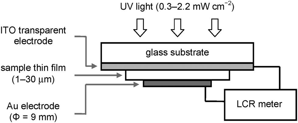 | ||
| Fig. 2 Experimental set-up for dielectric measurements under UV light irradiation at 365 nm. | ||
Results and discussion
Sample preparation and characterization
ATRP-initiator modified ZnO nanoparticles (ZnO–Br) were synthesized as shown in Fig. 1a, where the ZnO nanoparticles with an average diameter of 15 nm were used. In the first step, amine-functionalized ZnO nanoparticles (ZnO–NHMe) were prepared using a silane coupling reagent containing an aliphatic amine group. In the second step, ZnO–NHMe was reacted with an ATRP initiator with a benzyl bromide structure (BBnBiB),17 and the ATRP-initiator moiety was introduced on the ZnO surface (ZnO–Br). Methyl methacrylate was polymerized from ZnO–Br, and PMMA chains were grafted on the ZnO nanoparticles (PMMA–ZnO) as shown in Fig. 1b. Four kinds of core–shell nanoparticles with various PMMA chain lengths were synthesized as listed in Table 1. The volume fraction of ZnO ΦZnO for PMMA–ZnO was calculated using TG results (Fig. 3). Also, the grafting of the PMMA chains was recognized by high resolution SEM images in Fig. 4. After the grafting, the diameter of the core–shell nanoparticles becomes much larger than before.| Sample | Φ ZnO | PMMA shell thicknessb [nm] |
|---|---|---|
| a Calculated using a density of 5.22 g cm−3 for the ZnO nanoparticles and of 1.19 g cm−3 for the organic components. b Calculated from the average diameter of the ZnO nanoparticles (15 nm) and ΦZnO. | ||
| PMMA/ZnO | 0.054 | — |
| 0.105 | — | |
| 0.173 | — | |
| 0.239 | — | |
| PMMA–ZnO | 0.051 | 13 |
| 0.107 | 8.2 | |
| 0.172 | 6.0 | |
| 0.233 | 4.7 | |
 | ||
| Fig. 3 TG curves of (a) ZnO, (b) ZnO–Br, and (c) PMMA–ZnO with ΦZnO = 0.11 in an air flow. | ||
 | ||
| Fig. 4 High resolution SEM images of modified ZnO nanoparticles. (a) ZnO–Br. (b) PMMA–ZnO with ΦZnO = 0.11. | ||
Conventional nanocomposites (PMMA/ZnO) were also prepared by blending the ZnO–Br nanoparticles with PMMA, and designed to have the same ΦZnO as PMMA–ZnO. The two types of nanocomposite samples were molded by hot pressing. The dispersivity of the ZnO nanoparticles in the molded specimens was observed by SEM. Fig. 5 shows SEM images of the two types of nanocomposites with ΦZnO = 0.11. For PMMA/ZnO, the ZnO nanoparticles are inhomogeneously dispersed and form agglomerates with a submicron size. In contrast, the dispersivity of the ZnO nanoparticles is surprisingly good for PMMA–ZnO. In the PMMA–ZnO system, the ZnO nanoparticles are forced to be isolated and uniformly dispersed by the grafted PMMA shells.
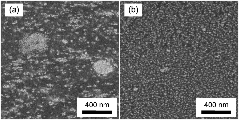 | ||
| Fig. 5 SEM images of cross-sections of two types of composites with ΦZnO = 0.11. (a) PMMA/ZnO. (b) PMMA–ZnO. | ||
Optical and dielectric properties of the molded samples
The difference in dispersivity of the ZnO nanoparticles between the two types of nanocomposites strongly influences light transmittance T. Fig. 6 shows the transmission spectra of the two types of nanocomposites in the λ range of 300–800 nm. Even at ΦZnO = 0.05, PMMA/ZnO exhibits almost zero T in the overall λ range. This is because the inhomogeneity of PMMA/ZnO causes intensive scattering of light. In contrast, PMMA–ZnO exhibits high transparency in the λ range of 400–800 nm in spite of the large thickness of ∼0.52 mm. The relatively low transparency in the lower λ range (400–600 nm) would be due to light scattering by the individual ZnO nanoparticles rather than absorption by the ZnO nanoparticles. On the other hand, almost zero T at less than 400 nm must be mainly attributed to absorption by the ZnO nanoparticles. According to the literature, ZnO has a wide band gap of 3.2 eV18 and therefore absorbs UV light less than 390 nm.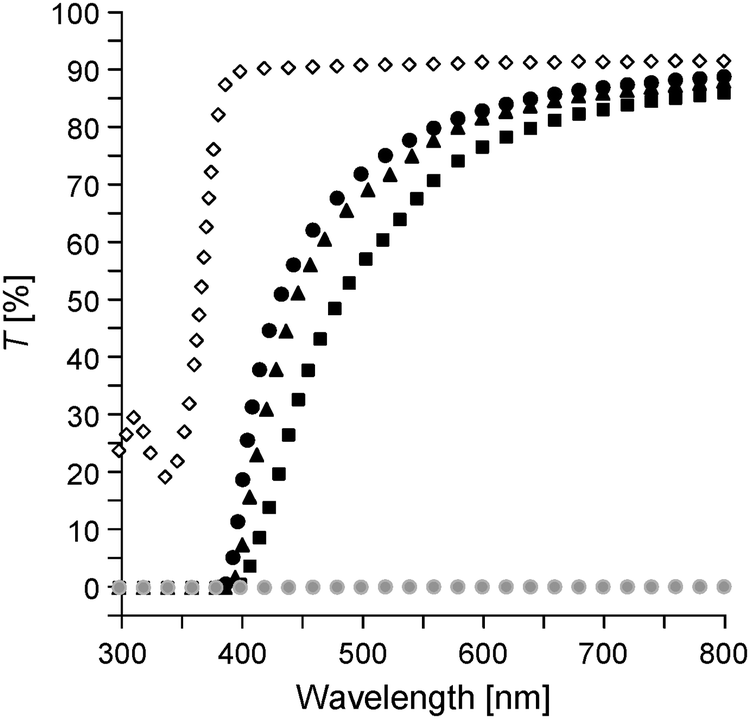 | ||
| Fig. 6 Transmission spectra of PMMA (diamonds) and two types of composites with ΦZnO = 0.05 (circles), ΦZnO = 0.11 (triangles), and ΦZnO = 0.23 (squares). Gray symbols, PMMA/ZnO; black symbols, PMMA–ZnO. The thickness of the specimens is around 0.52 mm. | ||
For dielectric measurements, gold electrodes were deposited on the molded specimens by sputter coating. In Fig. 7, εr′ and tanδ of the two types of nanocomposites at 1 kHz are plotted as a function of ΦZnO. Because of the low εr′ of ZnO (εr′ ≈ 10),26 both the nanocomposites have relatively low εr′s in comparison with PMMA/BaTiO3 composites.4,8,9 In addition, PMMA–ZnO has a smaller εr′ than PMMA/ZnO, resulting from the better dispersivity of the ZnO nanoparticles for PMMA–ZnO. The same phenomenon has already been reported for a PMMA/BaTiO3 composite system, and a detailed explanation is provided.9 Moreover, Wang and Tan have also demonstrated that a composite with agglomerated particles exhibited slightly higher εr′ than that with well-dispersed particles using a simulation method.39
 | ||
| Fig. 7 (a) Dielectric constant εr′ and (b) dissipation factor (tanδ) of PMMA (diamonds) and two types of composites at 1 kHz as a function of ΦZnO. Gray circles, PMMA/ZnO; black circles, PMMA–ZnO. | ||
Dielectric properties of the thin samples during UV light irradiation
As mentioned above, PMMA–ZnO is a promising material for UV light sensors using Δεr′ because of the strong absorption of UV light, low light scattering, and relatively low εr′. To demonstrate the potential for the capacitive UV light sensor, we set up a dielectric measurement system under UV light irradiation as shown in Fig. 2. In this measurement system, in order to irradiate UV light effectively on the sample, a transparent electrode made of ITO was used. The thickness of the sample was designed to be 1–30 μm using spin-coating from γ-butyrolactone solution. For the spin-coating of PMMA–ZnO, γ-butyrolactone was the best among general purpose solvents such as toluene, chloroform, tetrahydrofuran and DMF, which gave a clear and smooth thin film coated on the transparent ITO electrode. Fig. 8 shows εr′ and tanδ of the PMMA–ZnO thin films with ΦZnO = 0.17 at 1 kHz after UV light irradiation. As the UV light intensity becomes strong, the εr′ of PMMA–ZnO is highly increased. It is indicated that by absorption of UV light, electrons in the ZnO nanoparticles are excited from a valence band to a conductive band,18 resulting in large Δεr′ owing to Maxwell–Wagner polarization of the resultant free electrons.19 In addition, the εr′ of the PMMA–ZnO thin film becomes lower as the thickness is larger, suggesting that a thickness over 1 μm is too large for UV light to penetrate into the inside of the PMMA–ZnO thin films because UV light is strongly absorbed by the ZnO nanoparticles. Although we also tried to prepare PMMA–ZnO thin films with a thickness less than 1 μm, the reproducibility of the dielectric properties was poor probably because the thickness was excessively inhomogeneous. On the other hand, the tanδ of PMMA–ZnO is very low and almost constant as shown in Fig. 8b. This is because PMMA–ZnO is electrically insulated by the grafted PMMA chains on the ZnO nanoparticles. The ideal thickness of the PMMA shell is calculated from ΦZnO and the average diameter of the ZnO nanoparticles, and is listed in Table 1. The thick PMMA shell over 5 nm would prevent tunneling conduction between the ZnO nanoparticles by the free electrons according to an impedance analysis reported before.22 In this dielectric measurement, a PMMA/ZnO thin film with ΦZnO = 0.17 was also prepared, and the dielectric properties under UV light irradiation were evaluated in the same manner. During UV light irradiation with an intensity of 2.2 mW cm−2, the tanδ of the PMMA/ZnO thin film was over 10 which was out of the range of the used LCR meter. This extremely large dielectric loss is due to leak current by the free electrons.
 | ||
| Fig. 8 (a) Dielectric constant εr′ and (b) tanδ of PMMA–ZnO with ΦZnO = 0.17 at 1 kHz as a function of UV light intensity. The thickness of the PMMA–ZnO thin films is calculated to be 11 μm (circles), 4.2 μm (triangles), 2.0 μm (diamonds), and 1.0 μm (squares). | ||
Fig. 9 shows dielectric properties of PMMA–ZnO thin films with a thickness of about 1 μm at 1 kHz after UV irradiation with an intensity of 2.2 mW cm−2. The increase rate for the εr′ of PMMA–ZnO after UV irradiation R was calculated by the following equation: R = Δεr′/εr′0, where εr′0 is the εr′ of PMMA–ZnO before UV irradiation. Δεr′/εr′0 is more than 10% when ΦZnO > 0.1, which is large enough for the capacitive UV light sensor. Furthermore, the tanδ of PMMA–ZnO is less than 0.12 as shown in Fig. 9b although the tanδ value is increased when ΦZnO > 0.1. These results demonstrate that PMMA–ZnO has a high sensitivity and a low dielectric loss for the capacitive UV light sensor.
 | ||
| Fig. 9 Dielectric properties of PMMA–ZnO thin films with a thickness of about 1 μm at 1 kHz as a function of ΦZnO after UV irradiation with an intensity of 2.2 mW cm−2. (a) Increase rate for εr′ of PMMA–ZnO. The εr′ change Δεr′ is normalized by the εr′ before UV irradiation εr′0. (b) tanδ of PMMA–ZnO. | ||
For the application of a UV light sensor, the response speed of εr′ is also important. Fig. 10 shows the response speed of the εr′ of the PMMA–ZnO thin film with ΦZnO = 0.23 to UV irradiation with various intensities. The εr's are sharply increased right after UV irradiation and saturated in a few minutes during UV irradiation. When UV light turns off, the increased εr's are relaxed to the initial value in about 20 minutes. Owing to the low response speed for UV light irradiation, we suggest that the PMMA–ZnO thin films are used for a sunlight sensor that controls outdoor illumination for which no quick response is required. Because the UV intensity in sunlight is around 3 mW cm−2, PMMA–ZnO should have a sufficient sensitivity for sunlight. In fact, we have experimentally confirmed that PMMA–ZnO had a good sensitivity for sunlight. Further investigation on the capacitive UV light sensor using PMMA–ZnO is in progress.
 | ||
| Fig. 10 Response of εr′ at 1 kHz to UV irradiation with various intensities of 0.4 mW cm−2 (circles), 0.8 mW cm−2 (triangles), 1.3 mW cm−2 (diamonds), and 2.2 mW cm−2 (squares) for PMMA–ZnO with ΦZnO = 0.23. The thickness of the PMMA–ZnO thin film is 1.1 μm. | ||
Conclusion
In summary, a dielectric constant εr′-variable material with low dielectric loss was produced using polymer-grafted ZnO nanoparticles. In this study, a series of poly(methyl methacrylate)-grafted ZnO nanoparticles (PMMA–ZnO) were synthesized using a surface-initiated polymerization technique. The εr′ of PMMA–ZnO thin films was highly increased by irradiation of UV light. It is indicated that electrons in the ZnO nanoparticles are excited from a valence band to a conductive band by absorption of UV light, resulting in a highly increased εr′ owing to Maxwell–Wagner polarization of the resultant free electrons. On the other hand, the dissipation factor (tanδ) of PMMA–ZnO is very low and almost constant during UV irradiation because PMMA–ZnO is electrically insulated by the grafted PMMA chains on the ZnO nanoparticles. Also, it was confirmed that due to the grafted PMMA chains, PMMA–ZnO nanocomposites exhibited low light scattering in addition to strong absorption of UV light. The low light scattering of PMMA–ZnO would enhance the absorption efficiency of UV light and therefore contribute to the large increase in εr′ for PMMA–ZnO. Thus, PMMA–ZnO is a promising material for high sensitivity and low loss UV light sensors using the change in εr′.
References
- W. J. Sarjeant, J. Zirnheld, F. W. MacDougall, J. S. Bowers, N. Clark, I. W. Clelland, R. A. Price, M. Hudis, I. Kohlberg, G. McDuff, I. McNab, S. G. Parler Jr and J. Prymak, in Handbook of Low and High Dielectric Constant Materials and Their Applications, ed. H. S. Nalwa, Academic Press, London, 1999, vol. 2, ch. 9, pp. 423–491 Search PubMed.
- P. Kim, S. C. Jones, P. J. Hotchkiss, J. N. Haddock, B. Kippelen, S. R. Marder and J. W. Perry, Adv. Mater., 2007, 19, 1001–1005 CrossRef CAS.
- H. M. Jung, J.-H. Kang, S. Y. Yang, J. C. Won and Y. S. Kim, Chem. Mater., 2010, 22, 450–456 CrossRef CAS.
- L. Xie, X. Huang, C. Wu and P. Jiang, J. Mater. Chem., 2011, 21, 5897–5906 RSC.
- Y. Song, Y. Shen, H. Liu, Y. Lin, M. Li and C.-W. Nan, J. Mater. Chem., 2012, 22, 16491–16498 RSC.
- K. Hayashida and Y. Matsuoka, Carbon, 2013, 60, 506–513 CrossRef CAS.
- D. Wang, T. Zhou, J.-W. Zha, J. Zhao, C.-Y. Shi and Z.-M. Dang, J. Mater. Chem. A, 2013, 1, 6162–6168 CAS.
- K. Brandt, C. Neusel, S. Behr and G. A. Schneider, J. Mater. Chem. C, 2013, 1, 3129–3137 RSC.
- K. Hayashida, Y. Matsuoka and Y. Takatani, RSC Adv., 2014, 4, 33530–33536 RSC.
- Y. Feng, W. L. Li, Y. F. Hou, Y. Yu, W. P. Cao, T. D. Zhang and W. D. Fei, J. Mater. Chem. C, 2015, 3, 1250–1260 RSC.
- S. C. B. Mannfleld, B. C.-K. Tee, R. M. Stoltenberg, C. V. H.-H. Chen, S. Barman, B. V. O. Muir, A. N. Sokolov, C. Reese and Z. Bao, Nat. Mater., 2010, 9, 859–864 CrossRef PubMed.
- C. Metzger and E. Fleisch, Appl. Phys. Lett., 2008, 92, 013506 CrossRef.
- J. Li, J. Liang, L. Li, F. Ren, W. Hu, J. Li, S. Qi and Q. Pei, ACS Nano, 2014, 8, 12874–12882 CrossRef CAS PubMed.
- S.-J. Woo, J.-H. Kong, D.-G. Kim and J.-M. Kim, J. Mater. Chem. C, 2014, 2, 4415–4422 RSC.
- B. Nie, R. Li, J. Cao, J. D. Brandt and T. Pan, Adv. Mater., 2015, 27, 6055–6062 CrossRef CAS PubMed.
- W. Hu, Z. Ren, J. Li, E. Askounis, Z. Xie and Q. Pei, Adv. Funct. Mater., 2015, 25, 4827–4836 CrossRef CAS.
- Y.-S. Chen, G.-W. Hsieh, S.-P. Chen, P.-Y. Tseng and C.-W. Wang, ACS Appl. Mater. Interfaces, 2015, 7, 45–50 CAS.
- C. Kittel, in Introduction to Solid State Physics, ed. C. Kittel, John Wiley & Sons, New York, 7th edn, 1996, ch. 8, pp. 197–232 Search PubMed.
- A. Schönhals and F. Kremer, in Broadband Dielectric Spectroscopy, ed. F. Kremer and A. Schönhals, Springer-Verlag, Berlin, 2003, ch. 3, pp. 59–98 Search PubMed.
- S. F. Wang and A. A. Ogale, Compos. Sci. Technol., 1993, 46, 93–103 CrossRef CAS.
- K. Hayashida and H. Tanaka, Adv. Funct. Mater., 2012, 22, 2338–2344 CrossRef CAS.
- K. Hayashida, RSC Adv., 2013, 3, 221–227 RSC.
- K. Hayashida and Y. Matsuoka, Carbon, 2015, 85, 363–371 CrossRef CAS.
- A. Moezzi, A. M. McDonagh and M. B. Cortie, Chem. Eng. J., 2012, 185, 1–22 CrossRef.
- A. Kolodziejczak-Radzimska and T. Jesionowski, Materials, 2014, 7, 2833–2881 CrossRef CAS.
- N. H. Langton and D. Matthews, Br. J. Appl. Phys., 1958, 9, 453–456 CrossRef CAS.
- K. Hayashida, H. Tanaka and O. Watanabe, Polymer, 2009, 50, 6228–6234 CrossRef CAS.
- Z.-M. Dang, L. Z. Fan, S.-J. Zhao and C.-W. Nan, Mater. Sci. Eng., B, 2003, 99, 386–389 CrossRef.
- J. I. Hong, P. Winberg, L. S. Shadler and R. W. Siegel, Mater. Lett., 2005, 59, 473–476 CrossRef CAS.
- S. C. Tjong and G. D. Liang, Mater. Chem. Phys., 2006, 100, 1–5 CrossRef CAS.
- G.-S. Wang, Y. Deng, Y. Xiang and L. Guo, Adv. Funct. Mater., 2008, 18, 2584–2592 CrossRef CAS.
- H. Smaoui, L. E. L. Mir, H. Guermazi, S. Agnel and A. Toureille, J. Alloys Compd., 2009, 477, 316–321 CrossRef CAS.
- D. Ghosh, P. S. Sardar, M. Biswas, A. Mondal and N. Mukherjee, Mater. Chem. Phys., 2010, 123, 9–12 CrossRef CAS.
- G.-S. Wang, ACS Appl. Mater. Interfaces, 2010, 2, 1290–1293 CAS.
- S. Vural, S. Koytepe, T. Seckin and I. Adiguzel, Mater. Res. Bull., 2011, 46, 1679–1685 CrossRef CAS.
- W. Wu, X. Huang, S. Li, P.-K. Jiang and T. Tanaka, J. Phys. Chem. C, 2012, 116, 24887–24895 CAS.
- A. S. Roy, S. Gupta, S. Sindhu, A. Parveen and P. C. Ramanurthy, Composites, Part B, 2013, 47, 314–319 CrossRef CAS.
- N. Erdman, R. Campbeli and S. Asahina, Microsc. Today, 2006, 14, 22–25 Search PubMed.
- Y. U. Wang and D. Q. Tan, J. Appl. Phys., 2011, 109, 104102 CrossRef.
| This journal is © The Royal Society of Chemistry 2016 |