
Solution processed vertically stacked ZnO sheet-like nanorod p–n homojunctions and their application as UV photodetectors†
WonBae
Ko
a,
SangHyo
Lee
a,
NoSoung
Myoung
b and
JinPyo
Hong
*a
aResearch Institute of Convergence of Basic Science, Novel Functional Materials and Device Laboratory, Department of Physics, Hanyang University, Seoul 133-791, Korea. E-mail: jphong@hanyang.ac.kr
bAdvanced Photonics Research Institute (APRI), Gwangju Institute of Science & Technology (GIST), Gwangju 500-712, Korea
First published on 16th November 2015
Abstract
One long-standing goal in the development of one-dimensional nanostructured electronic devices is to facilitate the ongoing trend of miniaturization so as to enable ultralow power operation. Zinc oxide (ZnO) nanostructures, which have a direct and wide bandgap, are a central component in numerous electronic and optoelectronic applications. Here, we address vertically stacked ZnO sheet-like nanorod (SLNR) p–n homojunctions composed of single-crystalline undoped (n-type) and Li-doped (p-type) ZnO SLNRs by a multi-step solution-based hydrothermal route. Precise control of the molar concentration represented one of the basic factors in ensuring that the p–n homojunctions possessed appropriate densities and suitable morphologies. An extensive analysis of the luminescence features was carried out in order to identify p-type conduction in the Li-doped ZnO SLNRs. In addition, the SLNR-based p–n homojunctions exhibited distinct electrical features that validated their potential use as ultraviolet photodetectors, thereby spurring progress in the development of practical optoelectronics.
Introduction
One-dimensional (1D) ZnO semiconductor nanostructures, including ZnO nanowires (NWs) and nanorods (NRs), have been the focus of immense interest as one of the most reliable building blocks in current electronic and optoelectronic nanodevice applications. The widespread utilization of ZnO may be attributed to the desirable physical properties of the material, such as a wide direct band gap of 3.37 eV and a large exciton binding energy of approximately 60 meV at room temperature.1–7 To exploit such features, a variety of synthesis techniques, including molecular beam epitaxy (MBE), metalorganic chemical vapor deposition (MOCVD), and hydrothermal methods, have been employed to fabricate high-quality well-aligned 1D ZnO nanostructures.8–11 Among the various synthesis routes, the solution-based hydrothermal method has emerged as a promising alternative for use in simple, cost-effective large-scale fabrication processes. Solution-based procedures can be carried out at low temperature (<90 °C), and they allow for easy control of dopants so as to facilitate the development of various doped 1D ZnO nanostructures. However, one significant obstacle to the fabrication of suitable 1D p-type ZnO frames is the intrinsic n-type conductivity initially present in undoped ZnO during growth.12,13 Consequently, much effort has been devoted to the synthesis of 1D p-type ZnO nanostructures via the incorporation of various dopants to enhance semiconductor properties.14–16 It is widely believed that n-type conductivity behavior is dominant in undoped ZnO NWs and NRs due to the presence of intrinsic defects such as Zn interstitials, oxygen vacancies and hydrogen incorporation.17 Therefore, Li was selected for this study as a suitable candidate for the p-type doping of ZnO because Li has a small binding energy and Li is highly soluble in ZnO host materials. Furthermore, of the group I elements, Li has the smallest ionic radius (0.76 Å) for substitution into zinc sites (LiZn). The ionic radius of Li is also quite similar to that of Zn (0.74 Å), and thus, Li functions as a shallow acceptor in a substantial number of Zn sites.18 However, Li may easily occupy interstitial positions (Lii) due to its small ionic radius, thereby producing shallow donor states in ZnO.19–21 As a result, proper manipulation of the conduction type in various Li-doped ZnO nanostructures remains a challenge because of the presence of unintended defects introduced during growth. While numerous reports have been published on the successful use of dopants from group I (Li, Na, K), group V (N, P, As) and a mixture of doping elements to fabricate p-type ZnO NWs,18,22–25 the growth or design of vertically oriented ZnO sheet-like nanorod (SLNR) building blocks, which would provide new opportunities for future practical electronic devices, has not yet been demonstrated. Since the p–n photodetectors are expected to have several advantages, such as low dark current, fast responding speed and working without applied bias with respect to metal–semiconductor–metal (MSM) devices,23,26 the p–n photodetectors are becoming one of the most suitable building blocks for future optoelectronic applications.In this study, a hydrothermal synthesis procedure was employed to grow vertically stacked undoped ZnO (n-type)/Li-doped ZnO (p-type) SLNRs with designed physical properties. Control of the molar concentration and post-annealing conditions has a significant effect on the structural/optical features of p-type Li-doped ZnO SLNRs, as well as the electrical performance of the resulting in situ grown p–n homojunctions. The nature of the underlying conduction type after Li doping and high-temperature annealing is discussed through luminescence measurements, thereby providing valuable information on the design, fabrication, and optimization of future ZnO SLNR-based optoelectronic devices.
Experimental section
Synthesis of undoped ZnO NWs and SLNRs
To prepare pristine ZnO NWs on a 200 nm-thick SiO2 substrate, a 30 nm-thick ZnO thin film seed layer was first deposited onto the substrates by radio frequency (RF) plasma sputtering at room temperature. The deposited seed layer with a highly oriented, columnar morphology was then immersed in DI water containing a mixture of 0.025 M zinc nitrate hexahydrate (Zn(NO)3·6H2O, Sigma-Aldrich) and an equivalent molar concentration of hexamethylenetetramine (HMTA, Sigma-Aldrich). Here, the substrate was floated face down on the solution surface and allowed to react in a convection oven at 90 °C for 4 h. The choice of zinc nitrate and HMTA molar concentrations is a basic factor that governs the transformation between NWs and SLNRs. Therefore, to produce undoped ZnO SLNRs, a relatively high molar concentration of 0.15 M zinc nitrate and HMTA was employed (Fig. S1 in the ESI†).Synthesis of Li-doped ZnO SLNRs and p–n homojunctions
To synthesize Li-doped ZnO SLNRs, significant quantities of a 0.15 M lithium nitrate (Li(NO3), Sigma-Aldrich) solution were added to the previously described aqueous solution so as to introduce Li dopants during the growth. The as-grown Li-doped ZnO SLNRs were then heated to 600 °C in air for 10 min in order to activate Li dopants within the ZnO SLNRs. For the preparation of a ZnO p–n homojunction, the substrate was placed into a fresh solution containing the Li source for continued growth after processing the first n-type layer. As a result, multi-layer ZnO SLNRs with a thickness of ∼2 μm were obtained (Fig. 1d).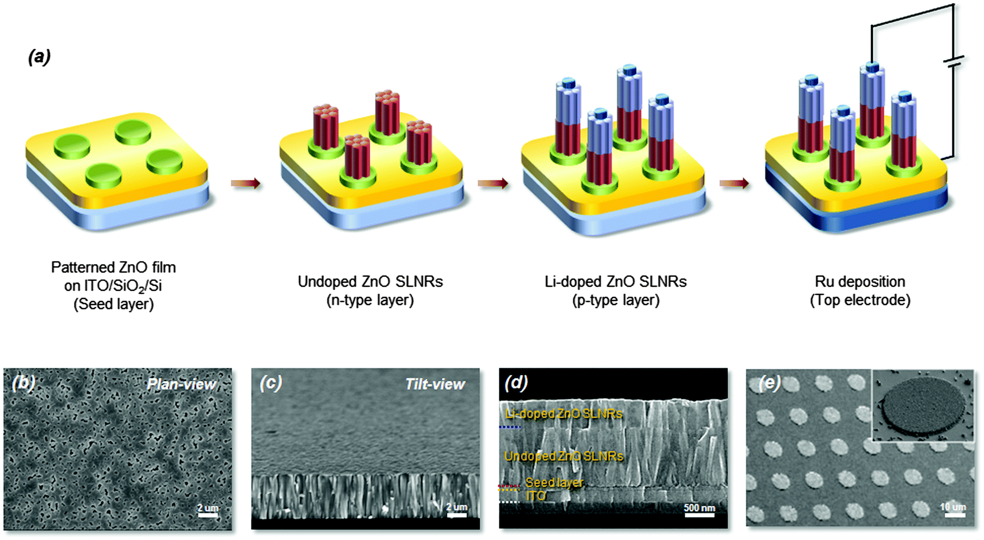 | ||
| Fig. 1 (a) Schematic flowchart of the fabrication process to produce ZnO SLNR p–n homojunctions (from left to right): patterned RF-sputtered ZnO seed layer, chemically grown undoped ZnO SLNRs (n-type), Li-doped ZnO SLNRs (p-type), and p–n homojunctions, respectively. Indium tin oxide (ITO) and ruthenium (Ru) were selected as electrodes to ensure ohmic contact with the undoped ZnO and Li-doped ZnO SLNRs, respectively. (b) Top-view SEM image of the ZnO seed layer, (c) tilted-view SEM image of the undoped ZnO SLNRs, (d) cross-sectional SEM image of vertically stacked ZnO SLNR p–n homojunctions, and (e) top-view SEM image of the patterned p–n homojunctions; a single patterned p–n homojunction is displayed in the inset. | ||
Characterization
The crystalline structure and morphology of undoped ZnO and as-grown/annealed Li-doped SLNRs were examined by field-emission scanning electron microscopy (FE-SEM, Hitachi S-4800), high-resolution X-ray diffractometry (HR-XRD, Rigaku), and high-resolution transmission electron microscopy (HR-TEM, JEOL JEM-2100F). To validate the luminescence properties for p-type conduction, photoluminescence (PL) spectroscopy was performed from 10 to 300 K using a 325 nm He–Cd laser line. Time-resolved photoluminescence (TRPL) spectroscopy was also conducted at 10 K using a mode-locked Ti:Sapphire layer (Chameleon Ultra II, Coherent Inc.) operating at 350 nm with a 150 fs pulse duration and a repetition rate of 80 MHz, with the 2nd harmonic produced by β-BaBO4 crystal in order to clearly elucidate the recombination dynamics from the observed emission features of the ZnO SLNRs. To evaluate the operation of the ZnO SLNR p–n homojunctions, indium tin oxide (ITO) and ruthenium (Ru) were selected as electrodes to ensure ohmic contact with the undoped ZnO and annealed Li-doped ZnO SLNRs, respectively; both electrodes were deposited via RF sputtering. The I–V characteristics of the structures were recorded using a Keithley 4200-SCS electrometer under dark and UV illumination conditions. A UV lamp (365 nm) was employed as the UV illumination source in order to evaluate the UV detection capabilities of the ZnO SLNR p–n homojunctions.Results and discussion
Shown in Fig. 1a is a schematic flowchart of the synthesis procedure (including electrode deposition) to produce ZnO SLNR p–n homojunctions on typical SiO2/Si substrates for potential UV photodetector applications. The ZnO SLNRs were fabricated via a simple hydrothermal process at low temperature without the use of additives such as polyethylenimine (PEI) or ammonium hydroxide (see above). For a comparison, undoped ZnO NWs were initially prepared on a ZnO thin film seed layer by hydrothermal synthesis (SEM images in Fig. S1 of the ESI†). The undoped ZnO NWs have a diameter of approximately 80 nm and grow preferentially in the c-axis direction (i.e., normal to the substrate) when the ZnO seed layer is not subjected to a thermal treatment. In our previous work, control of the ZnO seed layer conditions was found to have a profound impact on both the structural features of the synthesized ZnO NWs (e.g., morphology, grain size) and the in situ annealing process.27,28 In contrast, Fig. 1b and c display representative ZnO SLNRs with a relatively large diameter of 550 nm and a hexagonal (0001) sheet-like shape with flat and dense configurations. It is well known that, to meet the demands of vertically stacked ZnO p–n homojunctions, well-aligned, clean interfaces and morphologies must be established between the p–n junctions. In this work, precise manipulation of the ZnO SLNR morphology was achieved by adjusting the relative molar concentration of the ZnO source (see Fig. S2 in the ESI†). Ultimately, the proper concentration of zinc nitrate and HMTA for the development of SLNR p–n homojunctions was experimentally determined to be 0.15 M. Fig. 1d presents cross-sectional SEM images showing the well-faceted hexagonal SLNR homojunction end planes of ZnO segments; the ZnO SLNR layer, seed layer, and ITO film (bottom electrode) are denoted by blue, red, and yellow lines, respectively. As evident in the figure, continuous multi-step growth of ZnO SLNRs was carried out to enhance the electrical performance of the p–n homojunctions. In addition, the device size of the p–n homojunctions was defined through a typical photolithography process, producing periodic arrays with a spacing of approximately 10 μm (Fig. 1e). To produce p-type ZnO SLNRs, Li atoms were incorporated into the ZnO host material as p-type dopant sources for possible substitution of Zn cations during growth. The amphoteric behaviors of Li dopants in the ZnO lattice have been described in previous reports. In such cases, Li occupies octahedral sites (LiOi) in the empty cages of the ZnO wurtzite structure and subsequently acts as a donor, thereby maintaining or improving the initial n-type behavior of the material. However, when Li acts as an acceptor after being successfully substituted for Zn (LiZn), the Li-doped ZnO shows p-type conduction characteristics.20,21 Thus, post-annealing in the temperature range of 450–600 °C was employed for n- to p-type conduction conversion of the ZnO after Li doping.29 Undoped, as-grown Li-doped, and annealed Li-doped ZnO SLNRs were then systematically analyzed to gain insight into the designed physical properties.To clearly observe the crystalline features of the fabricated nanostructures, HR-TEM analyses were conducted with the assistance of a focused ion beam pre-treatment. The resulting images obtained for undoped, as-grown Li-doped, and annealed Li-doped ZnO SLNRs are shown in Fig. 2a–c, respectively; fast Fourier transform images corresponding to the areas highlighted by red rectangular boxes are displayed as insets. All of the ZnO SLNRs exhibit well-oriented single crystal wurtzite structures along the [0001] direction without obvious defects. However, the magnitude of the c-axis lattice constant in the as-grown Li-doped sample increased from 5.20 Å (the reference value corresponding to bulk ZnO) to 5.34 Å. Such an increase can primarily be attributed to the presence of Li atoms, which reside inside the cages of the ZnO wurtzite structure as interstitial dopants or defects.30 It is widely believed that Li atoms prefer to occupy the LiOi site in the empty cages of the ZnO wurtzite structure, while occupation at tetrahedral interstitial sites is not favorable (LiTi) since the formation energy of LiOi (Ef = −0.209 eV) is 0.62 eV lower than that of LiiT (Ef = −1.47 eV) in the nucleation process.31 In contrast, the c-axis lattice constant of the annealed Li-doped SLNRs decreased from 5.34 to 5.29 Å after post-annealing, reflecting the migration of Li atoms into the crystal lattice via thermal diffusion, followed by Li substitution of Zn (LiZn). To obtain indirect evidence of Li doping after post-annealing, electron energy loss spectroscopy (EELS) data were acquired for annealed Li-doped ZnO SLNRs using a 200 kV scanning transmission electron microscopy (STEM) system. Fig. 2d shows the Li-K edge peak (black line) extracted from the background signal (red line) at 60 eV, thus confirming the existence of Li within the ZnO SLNRs. The relatively weak intensity of the Li-K edge peak may be due to the low Li concentration provided during the doping process.32 Displayed in Fig. 2e are representative HR-XRD patterns for undoped (lower panel), as-grown Li-doped (middle panel), and annealed Li-doped (upper panel) ZnO SLNRs. All samples exhibit a single (002) diffraction peak at 34.4°, thereby demonstrating the presence of wurtzite phases preferentially oriented along the c-axis (in agreement with the SEM and TEM findings). Micro-Raman (μ-Raman) spectroscopy measurements were also carried out using a laser wavelength of 632.8 nm (Fig. S3 in the ESI†). All samples display representative E2 (high) and E2 (low) Raman active modes at 436 cm−1 and 100 cm−1, respectively; no additional lines or line splitting was noted in the spectra. The table at the bottom of Fig. S3 (ESI†) provides a summary of the full width at half maximum (FWHM) values for undoped, as-grown Li-doped, and annealed Li-doped ZnO SLNRs. The FWHM of the non-polar E2 (high) and E2 (low) modes gives information on the compressive strain in the samples due to Li incorporation.21 From the obtained results, it is expected that post-annealing allowed for lattice relaxation in the Li-doped ZnO SLNRs. This supports our previous assumption that Li occupies the empty cages of the wurtzite structure through thermal diffusion from interstitial (Lii) to substitutional (LiZn) sites. The results are also in agreement with the c-axis lattice constant variations observed in the TEM measurements.
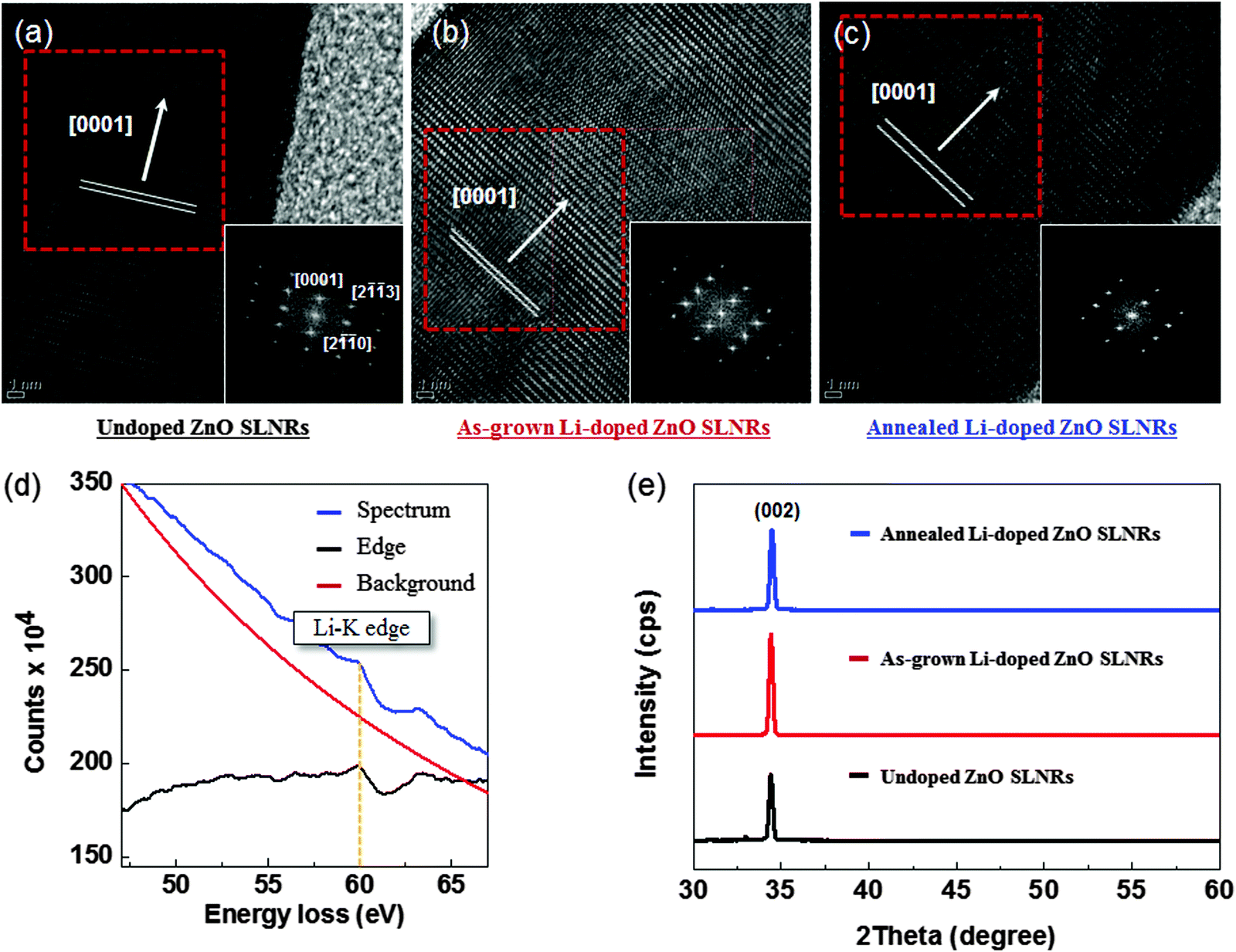 | ||
| Fig. 2 HR-TEM images obtained for (a) undoped, (b) as-grown Li-doped, and (c) annealed Li-doped ZnO SLNRs. The insets in (a)–(c) are the corresponding fast Fourier transform images. (d) EELS spectra of the annealed Li-doped ZnO SLNRs; a Li-K edge peak is clearly evident at 60 eV. The background signal was extrapolated from log polynomial law fitting. (e) HR-XRD patterns obtained for undoped (bottom, black line), as-grown Li-doped (middle, red line), and annealed Li-doped ZnO SLNRs (top, blue line); highly single crystalline (002) peaks are observed for all specimens. | ||
To gain further insight into the effect of Li-doping on the ZnO SLNRs, low-temperature PL data were obtained at 10 K using a 325 nm He–Cd laser. Representative PL spectra for undoped, as-grown Li-doped, and annealed Li-doped ZnO SLNRs are presented in Fig. 3a. Strong near-band-edge (NBE) electron transitions are observed at 3.352, 3.353, 3.360, and 3.364 eV, indicating the growth of high-quality ZnO SLNRs via hydrothermal processing. The undoped and as-grown Li-doped samples also exhibit peaks at 3.352 and 3.360 eV due to donor-bound exciton (DBX) recombination, while the annealed Li-doped sample displays peaks at 3.353 eV and 3.364 eV due to acceptor-bound exciton (ABX) and free exciton (FX) emissions, respectively.33 The strong DBX emission and weak FX emission responses of the undoped ZnO SLNRs suggest n-type conduction behavior. However, no LO phonon replicas associated with weak exciton–phonon coupling strength were detected for any of the ZnO SLNR specimens.34 A closer observation of the data reveals a blue shift in the NBE emission from the as-grown Li-doped ZnO SLNRs. It is likely linked with the presence of high free electron carrier densities provided by Li doping in the as-grown state.35,36 In contrast, post-annealing produces clear ABX emission and strong FX emission, suggesting acceptor behavior due to the substitution of Li for Zn atoms (LiZn). Upon examining the PL spectra in the visible region (Fig. S4 of the ESI†), the undoped ZnO SLNRs showed deep level emission (DLE) at 1.998 eV. Such a result can mainly be attributed to the presence of singly ionized oxygen vacancies (VO+).37 It is well-known that oxygen vacancies are native donor defects that contribute to the n-type conductivity of undoped ZnO. By adding Li dopants, DLE emission was gradually suppressed (Fig. S4 of the ESI†), indicating a reduction in structural defects and oxygen vacancies. It should be noted that no yellow emission associated with oxygen vacancies was observed in the annealed Li-doped ZnO SLNRs. This means that Li-related acceptors compensated donor defects (VO), and thus, the annealed Li-doped SLNRs show p-type conductivity. Post-annealing was conducted at 500, 550, and 600 °C (Fig. S5 of the ESI†), and distinct PL emission peaks arising from acceptor behavior were only observed at 600 °C. This implies that, for our particular case, Li dopants may only be activated above 600 °C. To gain additional insight into the luminescence features of annealed Li-doped ZnO SLNRs, low-temperature PL spectra were acquired at 10 K; the results are presented in Fig. 3b. The four peaks observed at 3.364, 3.353, 3.305, and 3.218 eV are associated with FX emission, ABX emission, free electron to acceptor transitions (e,A), and donor-to-acceptor pair (DAP) transitions, respectively.33,38,39 The acceptor energy of the Li dopant was estimated from the (e,A) transition at 3.305 eV using the expression E(e,A) = Eg(T) − EA + kBT/2,39 where Eg and EA are the band gap and acceptor energy levels, respectively, and kB is Boltzmann's constant. Since the thermal energy term can be neglected at 10 K, EA was estimated to be 132 meV when E(e,A) = 3.305 eV and Eg = 3.437 eV.40 Furthermore, the activation energy corresponding to the ABX emission peak was estimated to be 13 meV (Fig. S6 in the ESI†). The relationship between the acceptor energy level (EA) and the activation energy (EABXa) was consistent with Haynes rule. The shallow acceptor energy level of 132 meV and estimated activation energy level of 13 meV indicate that the Li dopants act as desirable acceptors in the ZnO SLNRs.
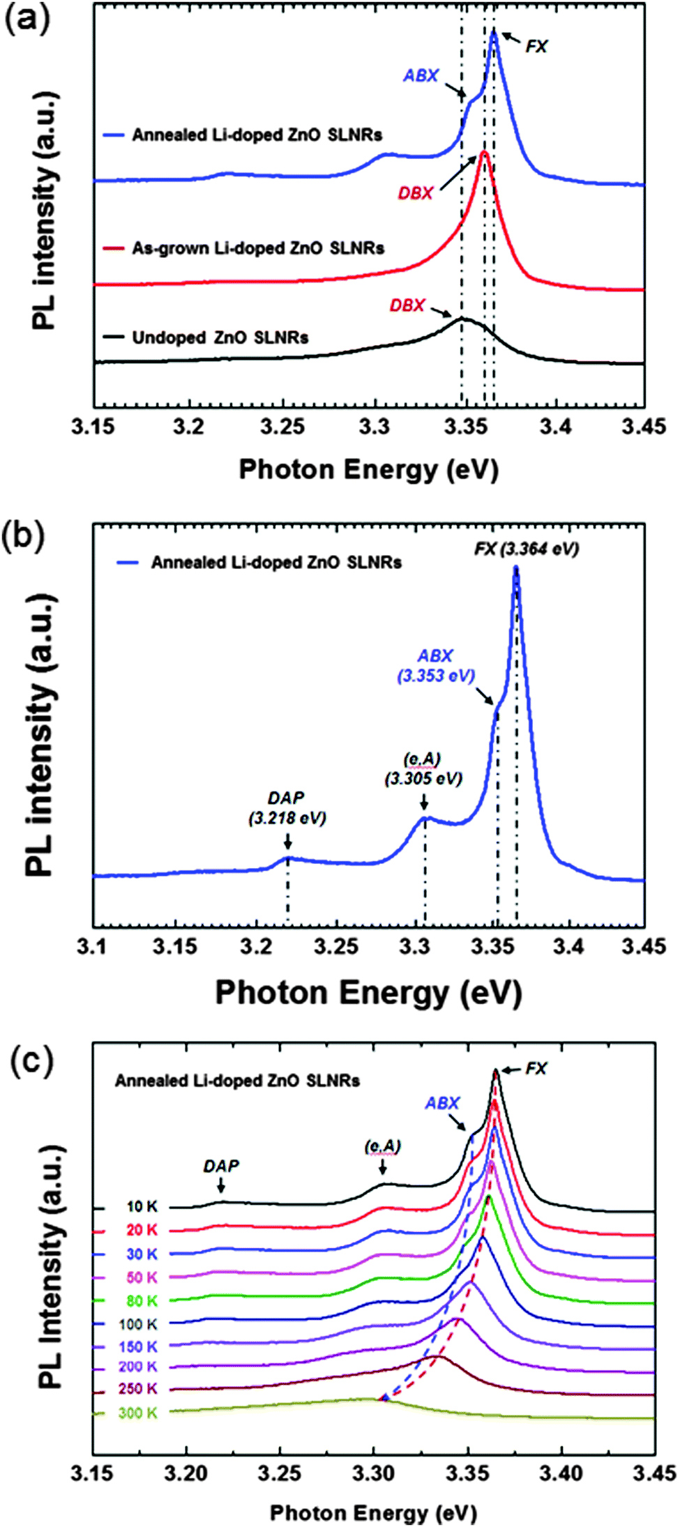 | ||
| Fig. 3 (a) Representative cryo-PL spectra of undoped, as-grown Li-doped, and annealed Li-doped ZnO SLNRs recorded at 10 K using a 325 nm source. (b) PL spectra of annealed Li-doped ZnO SLNRs, providing clear evidence that acceptor-bound excitonic emissions are responsible for p-type conduction. (c) Temperature-dependent PL spectra of annealed Li-doped p-type ZnO SLNRs in the range of 10 to 300 K. | ||
To further examine the structural features of the annealed Li-doped ZnO SLNRs, temperature-dependent PL measurements were conducted from 10 to 300 K; the results are shown in Fig. 3c. The ABX emission intensity rapidly decreases with a rise in temperature, and then disappears entirely at ∼150 K. FX emission is dominant at room temperature and exhibits a gradual redshift at higher temperatures. It should be noted that the FWHM of the emission increased with temperature, a finding that can be ascribed to exciton diffusion between different localized states at high temperatures.41,42 Enhanced emission efficiency may arise from enhanced crystalline or optical quality by preventing the migration of excitons toward non-radiative defects. This is the reason why the luminescence features of Li-doped ZnO improved significantly after the post-annealing treatment. Meanwhile, the photon energy from FX and ABX emission for the annealed Li-doped ZnO SLNRs decreases monotonically as the temperature increases. Such a trend can be well fitted by Varshini's equation (Fig. S7 of the ESI†).43
As detailed in the above discussion of the PL results, the migration of excitons toward non-radiative defects was prevented in the annealed Li-doped ZnO SLNRs, leading to an enhancement in the emission efficiency. To further exploit the nature of the recombination dynamics for the annealed Li-doped sample, TRPL measurements were conducted at 10 K using a 350 nm Ti:Sapphire laser as an excitation source and a picosecond streak camera (C11200, Hamamatsu Photonics); the results were subsequently fitted with the observed exponentials. Shown in Fig. 4a are the PL spectra of undoped and as-grown/annealed Li-doped samples. It is apparent that the spectra of the undoped and as-grown Li-doped samples are dominated by DBX emission, while the scan for the annealed Li-doped ZnO SLNRs is governed by FX, ABX, and (e,A) emissions. The time-resolved PL spectral plot used to determine exciton lifetimes is given in Fig. 4b. As evident in the figure, the undoped and as-grown Li-doped ZnO SLNRs exhibit fast DBX decay times of 75.8 and 71.8 ps, respectively. According to previous reports on undoped ZnO thin films,44 a fast recombination time of less than 74 ps is associated with the non-radiative recombination of non-radiative defects in ZnO, including vacancy complexes that include Zn vacancies.45 Therefore, as-grown Li-doped ZnO SLNRs displaying similarly short lifetimes are more likely to maintain non-radiative recombination centers when compared to undoped SLNRs. However, the annealed Li-doped ZnO SLNRs exhibit a much faster FX lifetime of about 40 ps. Bauer et al. reported a short time constant of several tens of ps in ZnO nanocrystals due to direct radiative recombination of FX.46 In addition, the radiative recombination lifetimes of (e,A) emissions, as determined by fitting bi-exponential decay curves, were found to be τ1 = 81 ps and τ2 = 822 ps. The longer lifetime of the annealed Li-doped ZnO SLNRs reflects a reduction in defects that serve as carrier traps. The table at the bottom of Fig. 4 summarizes the lifetimes of each peak observed for all samples.
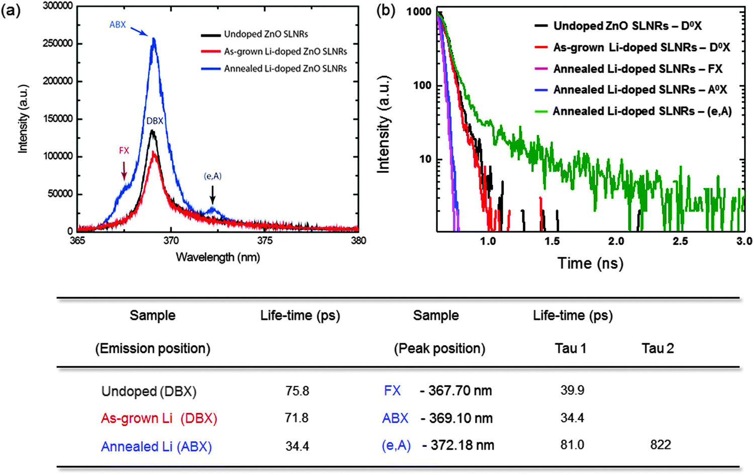 | ||
| Fig. 4 (a) PL spectra of undoped (black), as-grown Li-doped (red), and annealed ZnO (blue) SLNRs exposed to a 350 nm Ti:Sapphire excitation source; data were collected at 10 K. (b) Time-resolved PL responses of undoped ZnO (black line for DBX), as-grown Li-doped (red line for DBX), and annealed Li-doped ZnO SLNRs (purple line for FX, blue line for ABX, and green line for (e,A)). At the bottom of the figure is a table summarizing the time-resolved data observed for undoped, as-grown Li-doped, and annealed Li-doped ZnO SLNRs at 10 K. The lifetime of bound-exciton and acceptor-related emissions in the annealed Li-doped ZnO SLNRs provides evidence for the thermal activation of Li dopants upon annealing. | ||
In order to determine whether p-type conduction in the annealed Li-doped SLNRs can be generalized so as to extend the applicability of the structures, vertically stacked ZnO SLNR p–n homojunctions were constructed, and their electrical responses were recorded by scanning the voltage bias from −10 to +10 V. The I–V curves reflect typical rectifying behavior with a turn-on voltage of about 3.2 V, consistent with the electrical features observed for a ZnO-based diode with a band gap energy of 3.37 eV at room temperature. A high breakdown voltage of over 10 V was also noted. The I–V characteristics tested during a reversal in the polarity of the applied bias reflected the fact that the rectifying behavior arose from p–n homojunctions (not shown). The plots in the insets of Fig. 5 reveal linear I–V curves for both the ITO/n-ZnO SLNRs and Ru/p-ZnO SLNRs, thus confirming the formation of ohmic contacts. Semi-logarithmic I–V plots obtained under both forward and reverse biases are given in Fig. 5b. The forward current at +10 V and the reverse leakage current at −10 V are 1.29 × 10⁻³ A and 3.64 × 10⁻⁶ A, respectively, while the rectification ratio (defined as I(10 V)/I(−10 V)) was found to be 3.54 × 10². In addition, the ideality factors for the ZnO SLNR p–n homojunction diode were determined to be 2.5 in the low voltage regime (0 V < V < 1 V) and 10.3 in the high voltage regime (>1 V). The rectifying characteristics observed for the p–n homojunction diode are in good agreement with the results obtained from other p–n ZnO homojunction diodes containing high-quality p-type ZnO nanorods.47,48 This implies the presence of p-type conduction in the annealed Li-doped SLNRs of this study. It should be noted that all patterned p–n homojunction cells in Fig. 1e exhibit similar I–V behaviors, current levels, and rectification features (not shown).
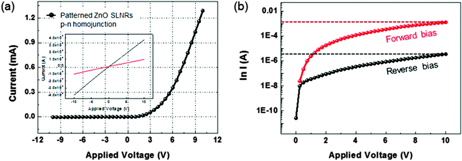 | ||
| Fig. 5 (a) I–V response of the vertically stacked ZnO SLNR p–n homojunctions; the turn-on voltage for an estimated junction area of ∼78.5 μm2 was approximately 3.2 V, while a high breakdown voltage of over 10 V was observed. (b) Semi-logarithmic I–V outputs revealing the presence of rectifying behavior in the ZnO SLNR p–n homojunctions under both forward and reverse biases; the rectification ratio was about 3.54 × 10² at 10 V. | ||
The I–V features of the vertically stacked ZnO SLNR p–n homojunctions measured under dark and illuminated (365 nm) conditions are displayed in Fig. 6; a schematic illustration of the homojunction device is provided in the inset. The ZnO homojunction device area, which was re-defined to allow for more effective light absorption, was approximately 100 μm × 20 μm. The p–n homojunction possesses a built-in potential so that electron–hole pairs generated by UV light in the depletion region can be dissociated. This in turn leads to the evolution of photocurrent. The charge carriers generated in the depletion region increased the conductivity of the p–n homojunction device, as demonstrated by the fact that both the forward and reverse currents increased with light illumination. Since the width of the depletion region is increased under reverse bias, the depletion capacitance is also decreased. Therefore, the responding speed and photo-gain of the photodetector can be enhanced. Consequently, the photogain, defined as the photocurrent divided by the dark current, was ∼5.4 at −10 V (reverse bias) and ∼1.2 at +10 V (forward bias) during testing with a light intensity of 25 mW cm−2.
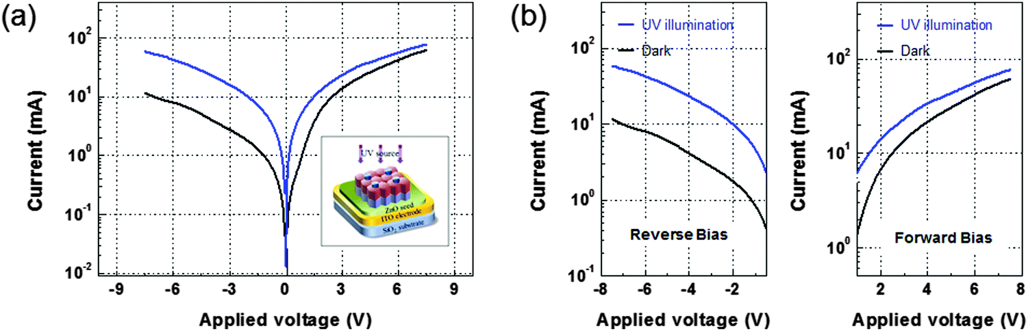 | ||
| Fig. 6 (a) I–V characteristics under dark conditions and after UV exposure and excitation of the vertically stacked ZnO SLNR p–n homojunctions; a schematic illustration of the homojunction device is shown in the inset. (b) Enlarged view of the I–V characteristics under both forward and reverse bias conditions. | ||
Conclusions
In summary, the growth of ZnO SLNRs and their resulting structural/electrical features, which are highly dependent on suitable doping and post-annealing, were investigated. The findings from detailed structural analyses provide evidence for the substitution of Zn by Li according to a thermally induced diffusion process during post-annealing. Such a scenario contributes to p-type conduction behavior. In addition, vertically stacked p–n homojunctions for potential optoelectronic device applications were prepared by a solution-based hydrothermal approach involving the multi-step growth of Li-doped (p-type) and undoped (n-type) ZnO SLNRs. The ZnO SLNR p–n homojunctions exhibited distinct electrical features that validated their use as possible UV photodetectors. We anticipate that the ability to control p-type conduction via hydrothermal doping will spur progress in the development of practical optoelectronic nanodevices.Acknowledgements
This work was supported by a grant from the National Research Foundation of Korea (NRF) funded by the Ministry of Education (NRF, No. 2013R1A1A2060350).Notes and references
- C. Soci, A. Zhang, B. Xiang, S. A. Dayeh, D. P. R. Aplin, J. Park, X. Y. Bao, Y. H. Lo and D. Wang, Nano Lett., 2007, 7, 1003–1009 CrossRef CAS PubMed.
- M. A. Zimmlar, T. Voss, C. Ronning and F. Capasso, Appl. Phys. Lett., 2009, 94, 241120 CrossRef.
- K. Y. Kim, J. U. Lee, S. Park, S. W. Kim, Z. L. Wang and J. M. Baik, ACS Nano, 2015, 9, 6394–6400 CrossRef CAS PubMed.
- M. S. M. Salifullah, K. R. V. Subramanian, D. J. Kang, D. Anderson, W. T. S. Huck, G. A. C. Jones and M. E. Welland, Adv. Mater., 2005, 17, 1757 CrossRef.
- J. J. Park, S. H. Lee, J. H. Lee and K. J. Yong, Adv. Mater., 2013, 25, 6423–6429 CrossRef CAS PubMed.
- H. E. Unalan, P. Hiralal, D. Kuo, B. Parekh, G. Amaratunga and M. Chhowalla, J. Mater. Chem., 2008, 18, 5909–5912 RSC.
- M. Y. Choi, D. Choi, M. J. Jin, I. S. Kim, S. H. Kim, J. Y. Choi, S. Y. Lee, J. M. Kim and S. W. Kim, Adv. Mater., 2009, 21, 2185–2189 CrossRef CAS.
- Y. W. Heo, B. S. Kang, L. C. Tien, D. P. Norton, F. Ren, J. R. La Roche and S. Pearton, Appl. Phys. A, 2005, 80, 497–499 CrossRef CAS.
- W. Lee, M. C. Jeong and J. M. Myoung, Acta Mater., 2004, 52, 3949 CrossRef CAS.
- L. E. Greene, M. Law, D. H. Tan, M. Montano, J. Goldberger, G. Somorjai and P. D. Yang, Nano Lett., 2005, 5, 1231 CrossRef CAS PubMed.
- J. J. Wu, H. I. Wen, C. H. Tseng and S. C. Liu, Adv. Funct. Mater., 2004, 14, 806 CrossRef CAS.
- W. J. Lee, J. Kang and K. Chang, Phys. Rev. B, 2006, 73, 024117 CrossRef.
- C. H. Park, S. B. Zhang and S. H. Wei, Phys. Rev. B: Condens. Matter Mater. Phys., 2002, 66, 073202 CrossRef.
- G. D. Yuan, W. J. Zhang, J. S. Jie, X. Fan, J. A. Zapien, Y. H. Leung, L. B. Lue, P. F. Wang, C. S. Lee and S. T. Lee, Nano Lett., 2008, 8, 2591–2597 CrossRef CAS PubMed.
- B. Xiang, P. W. Wang, X. Z. Zhang, S. A. Dayeh, D. P. R. Aplin, C. Soci, D. P. Yu and D. L. Wang, Nano Lett., 2007, 7, 323–328 CrossRef CAS PubMed.
- M. T. Chen, M. P. Lu, Y. J. Wu, J. H. Song, C. Y. Lee, M. Y. Lu, Y. C. Chang, L. J. Chou, Z. L. Wang and L. J. Chen, Nano Lett., 2010, 10, 4387–4393 CrossRef CAS PubMed.
- C. G. Van de Walle, Phys. Rev. Lett., 2000, 85, 1012 CrossRef CAS PubMed.
- J. S. Lee, S. N. Cha, J. M. Kim, H. W. Nam, S. H. Lee, W. B. Ko, K. L. Wang and J. P. Hong, Adv. Mater., 2011, 23, 4183–4187 CrossRef CAS PubMed.
- L. P. Carlos, D. Stefan, R. W. Markus, G. Melanie, H. Axel and P. Sebastian, CrystEngComm, 2014, 16, 1525–1531 RSC.
- M. D. McCluskey and S. J. Jokela, J. Appl. Phys., 2009, 106, 07110 CrossRef.
- M. G. Wardle, J. P. Goss and P. R. Briddon, Phys. Rev. B: Condens. Matter Mater. Phys., 2005, 71, 155205 CrossRef.
- P. Ruankham, T. Sagawa, H. Sakaguchi and S. Yoshikawa, J. Mater. Chem., 2011, 21, 9710 RSC.
- H. Shen, C. X. Shan, B. H. Li, B. Xuan and D. Z. Shen, Appl. Phys. Lett., 2013, 103, 232112 CrossRef.
- G. D. Yuan, W. J. Zhang, J. S. Jie, X. Fan, J. A. Zapien, Y. H. Leung, L. B. Luo, P. F. Wang, C. S. Lee and S. T. Lee, Nano Lett., 2008, 8, 2591 CrossRef CAS PubMed.
- G. Braunstein, A. Muraview, H. Saxena, N. Dhere, V. Richter and R. Kalish, Appl. Phys. Lett., 2005, 87, 192103 CrossRef.
- F. Sun, C. X. Shan, S. P. Wang, B. H. Li, Z. Z. Zhang, C. L. Yang and D. Z. Shen, Mater. Chem. Phys., 2011, 129, 27 CrossRef CAS.
- W. B. Ko, S. H. Lee, J. S. Lee and J. P. Hong, J. Nanosci. Nanotechnol., 2012, 12, 6036–6039 CrossRef CAS PubMed.
- K. Panita, H. Mati, B. Kanittha, S. Nuttapun, P. Panida, K. Wiyong, S. Armote, W. Jutaphet, P. Sirapat, P. Supanit and K. Annop, Phys. Status Solidi A, 2015, 212, 394–400 CrossRef.
- B. K. Meyer, N. Volbers, A. Zeuner, S. Lautenschlager, J. Sann, A. Hoffmann, U. Haboeck, MRS symposia Proceedings No. 891, Materials Research Society, Pittsburgh, 2006.
- C. L. Tsai, M. S. Wang, Y. H. Chen, H. C. Chang, C. J. Liu, C. T. Lee, Y. T. Shih, H. J. Huang and Y. U. Lin, J. Appl. Phys., 2010, 107, 113717 CrossRef.
- A. Carvalho, A. Alkauskas, A. Pasquarllo, A. K. Tagantsev and N. Setter, Phys. Rev. B: Condens. Matter Mater. Phys., 2009, 80, 195205 CrossRef.
- F. Wang, J. Graetz, M. S. Moreno, C. Ma, L. Wu, V. Volkov and Y. Zhu, ACS Nano, 2011, 5, 1190–1197 CrossRef CAS PubMed.
- A. Teke, U. Ozgur, S. Dogan, X. Gu and H. Morkoc, Phys. Rev. B: Condens. Matter Mater. Phys., 2004, 70, 195207 CrossRef.
- R. Chen, Q. Ye, T. He, V. D. Ta, Y. J. Ying, Y. Y. Tay, T. Wu and H. Sun, Nano Lett., 2013, 13, 734–739 CrossRef CAS PubMed.
- T. Sakai, T. Kakeno, T. Ikari, S. Shirakata, T. Sakemi, K. Awai and T. Yamamoto, J. Appl. Phys., 2006, 99, 043508 CrossRef.
- S. C. Jain, J. M. McGregor and D. J. Roulston, J. Appl. Phys., 1990, 68, 3747 CrossRef CAS.
- M. K. Partra, K. Manzoor, M. Manoth, S. R. Vadera and N. Kumar, J. Lumin., 2008, 128, 267 CrossRef.
- O. Kobayashi, F. Sankey and J. D. Dow, Phys. Rev. B: Condens. Matter Mater. Phys., 1983, 28, 946 CrossRef.
- M. Schirra, R. Schneider, A. Resiser, G. M. Prinz, M. Feneberg, J. Biskupek, U. Kaiser, C. E. Krill, K. Thonke and R. Sauer, Phys. Rev. B: Condens. Matter Mater. Phys., 2008, 77, 125215 CrossRef.
- D. K. Hwang, H. S. Kim, J. H. Lin, J. Y. Oh, J. H. Yang, S. J. Park, K. K. Kim, D. C. Look and Y. S. Park, Appl. Phys. Lett., 2005, 86, 151917 CrossRef.
- H. D. Sun, M. Hetterich, M. D. Dawson, Y. A. Egorov, D. Bernklau and H. Riechert, J. Appl. Phys., 2002, 92, 1380 CrossRef CAS.
- R. Chen, S. Phann, H. D. Sun, Q. Zhuang, M. R. Godenir and A. Krier, Appl. Phys. Lett., 2009, 95, 261905 CrossRef.
- Y. P. Varshini, Physica, 1967, 34, 149–154 CrossRef.
- U. Ozgur, A. Teke, C. Liu, S. J. Cho, H. Morkoc and O. Everitt, Appl. Phys. Lett., 2004, 84, 3223 CrossRef CAS.
- T. Koida, S. F. Chichibu, A. Uedono, A. Tsukazaki, M. Kawasaki, T. Sota, Y. Segawa and H. Koinuma, Appl. Phys. Lett., 2003, 82, 532 CrossRef CAS.
- C. Bauer, G. Boschloo, E. Mukhtar and A. Hagfeldt, Chem. Phys. Lett., 2004, 387, 176 CrossRef CAS.
- H. M. Chiu, Y. T. Chang, W. W. Wu and J. M. Wu, ACS Appl. Mater. Interfaces, 2014, 6, 5183–5191 CAS.
- Y. Yang, X. W. Sun, B. K. Tay, G. F. You and S. T. Tan, Appl. Phys. Lett., 2008, 93, 253107 CrossRef.
Footnote |
| † Electronic supplementary information (ESI) available. See DOI: 10.1039/c5tc02977e |
| This journal is © The Royal Society of Chemistry 2016 |