Structure engineering of a core/shell Si@Ta3N5 heterojunction nanowires array for photoelectrochemical water oxidation

Ping Wang*ab and Jae Sung Lee*b
aSchool of Materials Science and Technology, University of Shanghai for Science and Technology, Shanghai, 200093, P. R. China. E-mail: ping.wang@usst.edu.cn
bSchool of Energy & Chemical Engineering, Ulsan National Institute of Science & Technology (UNIST), Ulsan, 689798, South Korea. E-mail: jlee1234@unist.ac.kr

Received 29th September 2016 , Accepted 28th October 2016

First published on 28th October 2016


Abstract

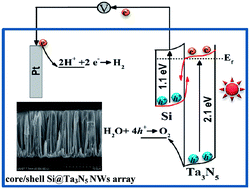
Structure-tuned core/shell n-Si@n-Ta3N5 nanowires array heterojunction photoanodes were prepared on a wafer scale by electroless metal-assisted etching of an Si wafer, spin coating of a Ta(OC2H5)5 sol precursor solution, and ammonia treatment to convert it to Ta3N5. The length of the Si NWs and the thickness of the Ta3N5 shell were critical variables to control the high photoelectrochemical water splitting performance of the photoanode. The photocurrent density of the optimum core/shell Si@Ta3N5 nanowires array was 2.5 times higher than that of the planar Si@Ta3N5 composite at 1.23 VRHE under 1 sun illumination. The Ta3N5 nanoshell served as a protection layer to significantly improve the chemical stability of the Si photoelectrode, and acted as a component to form a heterojunction with Si to promote the transport and separation of photoexcited charge carriers.


Introduction

Photoelectrochemical (PEC) water splitting using semiconductor photocatalysts offers an attractive path to directly solve energy and environmental problems by conversion of solar energy into hydrogen fuel.1–3 A large number of semiconductor materials have been explored as photoelectrodes or powdered photocatalysts,4,5 the solar-to-hydrogen (STH) conversion efficiencies of these traditional materials are still not high enough. Nanostructuring of semiconductor materials, especially into one dimensional (1D) nanostructures has been a popular strategy to obtain enhanced solar energy conversion efficiency because of improved light attenuation, promoted transport and separation of photoexcited charge carriers, and abundant surface reaction sites.6,7

Silicon (Si) has been extensively studied in the electronics and photovoltaic (PV) industries, because of its abundance in the earth's crust and a small band gap energy (Eg = ∼1.12 eV) suitable for efficient visible light harvesting.8 But for PEC cell applications, the use of Si remains a major challenge as strong reflection of incident light from the water–silicon substrate interface due to the high reflective index of Si and rapid formation of a thin insulating oxide layer in aqueous solutions resulting in surface passivation. Moreover, due to its high valence band maximum energy, it is thermodynamically impossible to oxidize water spontaneously and a high anodic bias is needed to overcome the high overpotential loss for the water oxidation process. In order to address these fundamental issues, proper design of black Si nanowires (NWs) array-based heterojunction semiconductor has been proposed by covering the Si NWs surface with a desired semiconductor.9 In 2009, Yang and the co-workers prepared n- or p-type Si/n-TiO2 NWs array, demonstrating that n-Si/n-TiO2 showed a larger photocurrent and open circuit voltage than p-Si/n-TiO2 NWs array, and 2.5 times photocurrent enhancement compared to planar Si/TiO2 structure due to their low reflectance and high surface area.10 In 2011, Shi et al. reported the photoconversion efficiency for the as-prepared Si/ZnO NWs array reaches 0.38% upon exposure to the illumination with a light intensity of 10 mW cm−2, which is higher than those of the planar bilayer structure of Si/ZnO (0.19%) and the pure planar ZnO (0.09%).11 In 2012, Yang and the co-workers found the photocurrent enhancement by 5 times on the case of hierarchical Si/InGaN NWs array compared to the photocurrent density of InGaN grown on planar Si. It was attributed to single phase InGaN nanowires grown vertically on the sidewalls of Si wires acting as a high surface area photoanode for solar water splitting.9,12 Most recently, successful results on the Si/NiOx NWs photoanode system have also been obtained.13 In the cases, it was demonstrated that architecture of n/n nanowire heterojunctions not only suppressed the surface corrosion and reflection of Si, but also provided a junction photovoltage and thus markedly promoted the charge separation for photo-oxidation of water.14 On the other hand, in the on-going search for suitable photoanode materials, tantalum nitride (Ta3N5) as a new n-type semiconductor has attracted an increasing amount of attention as a promising water splitting photocatalyst, because it has a band gap of ∼2.1 eV capable of absorbing a large portion of the incident solar spectrum (up to 600 nm) and suitable band positions for water splitting reaction.15 However, it is unstable in the highly oxidative environments of water oxidation,16,17 and no studies are reported on its nanowire array geometry.

Herein, with these design principles in mind, we prepared for the first time a n/n type core/shell Si@Ta3N5 NWs array for PEC water oxidation. The influences of the length of Si nanowire core and the thickness of Ta3N5 shell were detailed investigated on the structural and optical properties of the Si@Ta3N5 NWs array. The results demonstrated that the nanostructure heterojunction is of great importance to enhance the PEC water oxidation performance. The structure-optimized core/shell Si@Ta3N5 NWs array exhibited 2.5 times higher photocurrent density that of a planar Si@Ta3N5 composite. The enhanced performance of the core/shell Si@Ta3N5 NWs array was attributed to its 1D nanostructure, which greatly enhanced the surface area and light attenuation, and promoted the transport and separation of photoexcited charge carriers.

Experimental

Fabrication of core/shell Si@Ta3N5 nanowires array

Scheme 1 shows an illustrative synthetic scheme for fabrication of core/shell Si@Ta3N5 NWs array. First, vertically aligned n-type Si NWs array on the silicon wafers were prepared by metal-assisted chemical etching of a polished Si(100) wafer (P doped, TEST, 1–30 Ω cm, 675 μm) at room temperature (RT) according to a procedure reported previously.10,18,19 The wafer (4 × 3 cm2) was ultrasonically degreased in acetone (J. T. Baker) and ethanol (Baker Analyzed reagent) each for 10 min at RT, and then was chemically oxidized in a boiled H2SO4/H2O2 solution (3[thin space (1/6-em)]:[thin space (1/6-em)]1, Sigma-Aldrich) for 10 min. After each cleaning step, the wafer was rinsed with excess deionized water. The cleaned Si wafer piece was then immersed in 10% HF solution for 5 min to remove the thin oxide layer on the surface, and into the aqueous etching solution containing 0.04 M AgNO3 (99.0%, Sigma-Aldrich) and 5 M HF (48–51%, J. T. Baker) at RT for a designed etching time. After washing the resulting Ag dendrites and crystals on Si NWs surface in a concentrated HNO3 bath (69%, Sigma-Aldrich) for at least 30 min, large-area vertically aligned Si NWs could be observed on the dark silicon substrate surface. The length of the Si NWs can be tuned by the etching time and the as-prepared Si NWs samples with different etching times of 15, 30 and 60 min are designed as nSi15, nSi30, and nSi60, respectively.
image file: c6ra24263d-s1.tif
Scheme 1 An illustrative synthetic scheme for fabrication of core/shell Si@Ta3N5 NWs array.

Core/shell Si@Ta3N5 NWs array was obtained via a facial spinning coating deposition of a Ta(OC2H5)5 sol precursor solution. The sol precursor solutions of (0.2–1 M) were prepared by mixing Ta(OC2H5)5 (99.98%, Sigma-Aldrich) with 1 mL C2H5OH and 50 μL CH3COOH (99.7%, Sigma-Aldrich) and vigorously stirring for 1 h. Before coating, the obtained Si NWs array was chemically etched in 50[thin space (1/6-em)]:[thin space (1/6-em)]1 HF solution (containing one part of 49% HF and 50 parts of deionized water) to remove oxide layer for 1 min. Then, 100 μl of the prepared precursor solution was dropped at the center of the Si NWs array substrate and spin-coated at 3000 rpm for 30 s. The spin coating process was repeated two times and then dried at 80 °C for 2 h. Next, the coated Si NWs array samples were further treated in an alumina tube furnace in NH3 (99.99995%) with a flow rate of 100 mL min−1 at ∼900 °C for 6 h to form Ta3N5. The resulting samples were denoted using etching time and concentrations of Ta(OC2H5)5 sol precursor solution (0.2–1 M). Thus, nSi60-1/4 indicates nSi60 NWs coated by 1 M of Ta(OC2H5)5 sol precursor solution for 4 times. As a reference, a planar Si/Ta3N5 composite structure was synthesized in a three-step process involving RF magnetron sputtering of Ta metal, thermal oxidation and then nitridation. Briefly, a desired thickness of Ta metal was deposited by RF magnetron sputtering on Si silicon wafers. The deposited Si wafers were inserted into a hot oven held at 550 °C for 5 min in air and then, nitridated in the alumina tube furnace under the same experimental conditions as above.

Characterization

The X-ray diffraction (XRD) patterns of all samples were recorded with a X-ray diffractometer (X'Pert PRO MPD, PANalytical) with a monochromated Cu Kα (λ = 0.1541 nm) radiation at 40 kV and 30 mA, and the data were collected from 10° to 80° (2θ). The film samples were examined in scanning electron microscopes (SEM) using a field emission (FE)-SEM (JEOL JSM-7401F, JEOL). High-resolution transmission electron microscopy (HRTEM), high resolution aberration-corrected scanning transmission electron microscopy (STEM) and energy dispersive X-ray spectroscopy (EDS) were performed on a JEOL JEM-2100F/CESCOR electron microscope equipped with a field-emission gun operating at 200 kV. For TEM measurements, the samples were prepared by dispersing the scratched powders from the film as a slurry in ethanol, which were dispersed and dried on a porous carbon film on a Cu grid.

Photoelectrochemical measurements

PEC measurements were carried out in a standard three-electrode configuration, where the prepared films, Pt mesh rod and Ag@AgCl electrode acted as working, counter and reference electrodes, respectively. Aqueous 0.5 M Na2SO4 (pH 6.5), 0.1 M potassium phosphate (KPi, pH 7.0) and 1 M NaOH (pH 13.6) solutions were tested as electrolytes. All electrochemical data were recorded by using a potentiostat (IviumStat, Ivium Technologies). The scan rate for the current (I)–voltage (V) curve was 10 mV s−1. A 300 W xenon lamp was used as a solar simulator (Oriel 91160) with an AM 1.5G filter calibrated with a reference cell certified by the National Renewable Energy Laboratories, USA. The measured potentials vs. Ag/AgCl were converted to the reversible hydrogen electrode (RHE) scale, according to the Nernst equation (ERHE = EAg/AgCl + 0.059 pH + EoAg/AgCl), where ERHE is the converted potential vs. RHE, EAg/AgCl is the experimentally measured potential against the Ag/AgCl reference electrode and EoAg/AgCl = 0.1976 V at 25 °C. The applied bias photon-to-current efficiency (ABPE) was calculated from the IV curves using the following equation:20,21 ABPE = I(1.23 − V)/Jlight, where V is the applied bias vs. RHE, I is the photocurrent density at the measured bias, and Jlight is the incident light intensity of 100 mW cm−2 (AM 1.5G).

Results and discussion

Synthesis and characterization of core/shell Si@Ta3N5 NWs array films

Fig. 1 shows the normalized X-ray diffraction patterns (XRD) of the pristine nSi30 NWs sample, the as-synthesized core/shell Si@Ta3N5 NWs array films with different lengths of nSi NWs and thicknesses of Ta3N5 shell, and the Si/Ta3N5 planar composite film. The diffraction reflections from Si substrate can be clearly observed in the XRD patterns of all samples. The strongest diffraction peak at 2θ ≈ 69.2° corresponds to the Si(400) planes of Si, indicating a strong orientation along the c axis of Si substrate. The additional small peaks at 2θ ≈ 33.0° and 65.9° can be indexed as Si(200) and Si(332) planes, respectively, and the diffraction peak appeared at 2θ ≈ 61.7° can be assigned to Si(004) plane as a result of the Cu Kβ radiation diffracted from the Si(400) planes.22,23 Other peaks observed for the core/shell Si@Ta3N5 nanowire arrays films can be indexed only as a single orthorhombic Ta3N5 phase, which corresponds exactly to the standard XRD pattern (JCPDS 19-1291 card). It is worthy to note that no obvious shift of the diffraction peaks is observed, and the Si-barrier species (SiO2 and Si3N4, etc.) are not distinctly identified. It was demonstrated that the possible nitridation of Si NWs can be greatly suppressed once the Ta3N5 shell is formed on the surface during ammonia treatment and acts as a dense protection layer.24 With the increased concentration of the spin-coated Ta(OC2H5)5 sol precursor from 0.2 M to 1 M, the XRD peak intensity of the obtained Ta3N5 phase increased gradually in the samples of nSi15-0.2, nSi15-0.5 and nSi15-1. Similarly, the longer Si NWs resulted in an increased amount of tantalum ethoxide sol precursors coated on the Si NWs surface, as reflected on the stronger peak intensities of the Ta3N5 phase. No Ta3N5 phase was observed in the XRD pattern of the planar Si/Ta3N5 composite film, probably below the detection limit of the XRD analysis.
image file: c6ra24263d-f1.tif
Fig. 1 Normalized X-ray diffraction patterns (XRD) of the representative nSi30 NWs sample, the as-synthesized core/shell Si@Ta3N5 NWs array, and the Si/Ta3N5 planar composite film, respectively.

Fig. 2 shows representative cross-sectional SEM images of (a) nSi15, (b) nSi30 and (c) nSi60 samples, respectively. After etching in the AgNO3/HF etching solution for 15, 30 and 60 min, respectively, the lengths of the formed Si NWs array on the Si wafer substrate were ca. 3.2, 6.0 and 11.9 μm for the nSi15, nSi30 and nSi60 samples, respectively, demonstrating that the length of the Si NWs can be easily controlled by the etching time with an etching rate of ca. 0.2 μm min−1. The estimated diameters of the as-synthesized Si NWs are in a few nanometers to submicrometer range. As seen in the surface and cross-sectional SEM images in Fig. 2d–i, several individual Si@Ta3N5 core/shell NWs form clusters of NWs arrays. Each Si NW surface was tightly covered by a Ta3N5 layer. The surface and cross-sectional SEM images of nSi15-0.2, nSi15-0.5 and nSi15-1 samples in Fig. S1 in the (ESI) revealed that a higher concentration of Ta(OC2H5)5 sol precursors resulted in a thicker Ta3N5 shell, which is consistent with the above XRD results. Therefore, the results demonstrated that the dimensions of core/shell Si@Ta3N5 NWs can be readily controlled by adjusting the synthetic conditions. A representative cross-sectional SEM image of the Si/Ta3N5 planar composite film is presented in Fig. S2.


image file: c6ra24263d-f2.tif
Fig. 2 Representative cross-sectional SEM images of (a) nSi15, (b) nSi30 and (c) nSi60 NWs array, and representative cross-sectional and surface SEM images of (d and e) nSi15-0.5, (f and g) nSi30-0.5 and (h and i) nSi60-0.5 NWs array, respectively.

Fig. 3 shows representative low-magnification TEM and HRTEM images of the as-synthesized nSi60-0.5 sample. As seen in Fig. 3a, the nSi60-0.5 sample is composed mainly of the nanowires with diameters of tens of nanometers. It also contains submicrometer debris scratched from the bottom of slightly etched Si wafer. Fig. 3b shows the HRTEM lattice image of a single nanowire with a core/shell structure. The Ta3N5 shell perfectly covered the Si core and a smooth interface is formed between the Ta3N5 and Si. The (110) atomic planes of the Ta3N5 with lattice spacing of ∼0.36 nm can be clearly identified. The observed structure was further confirmed by HAADF-STEM-EDX mappings. As shown in Fig. 4, HAADF-STEM image and corresponding EDX elemental mapping of the as-synthesized nSi60-0.5 (Fig. 4a–d) reveals that Ta and N elements are homogenously distributed in the outer region of the observed nanowire. The Si element mapping shows the distribution of low concentration of Si in the outer region of the observed nanowires in addition to the high Si concentration core of the nanowire, which is also revealed by the element-sensitive EDS line scan (position indicated by lines in (a)) in Fig. 4e. The result indicates that due to self-diffusion of Si during the thermal annealing,25–27 some Si atoms have diffused into in the Ta3N5 shell. In contrast, there is no diffusion of Ta or N atoms into the Si NWs core.


image file: c6ra24263d-f3.tif
Fig. 3 Representative TEM (a) and HRTEM images (b) of the as-synthesized nSi60-0.5 sample.

image file: c6ra24263d-f4.tif
Fig. 4 STEM/EDX elemental mapping of the as-synthesized nSi60-0.5 sample: (a) HAADF-STEM image, (b–d) EDS mapping images of Si, Ta and N elements, respectively. (e) Element-sensitive EDS line scan image (position indicated by a line in (a) giving relative atomic concentrations for Si, Ta and N elements).

The UV-visible absorption spectra of the as-prepared prototypical samples (nSi30, nSi60 and nSi60-0.5) are shown in Fig. S3. The as-prepared Si NWs array have good light absorption ability, due to its favourable hierarchical structure and low energy gap, and the long Si NWs of nSi60 have more light-trapping effect than the short Si NWs of nSi30 as the reflectance decreases with increasing wire length, which are in good agreement with the reported results.28,29 More importantly, it can be seen that compared with the single nSi60 NWs array alone, incorporation of Ta3N5 to nSi NWs in nSi60-0.5 samples significantly increased light absorption, exhibiting excellent absorption capacity to the sunlight spectrum the range of 300–800 nm. It can be attributed to the beneficial effect of core/shell Si@Ta3N5 hierarchical structure as dual band-gap light absorber. As a result, a certain fraction of the reflected light would fall upon another area of the nanosystem in such a NW array structure and be harvested more efficiently, instead of being lost to free space.

Effect of Si NWs core length

Fig. 5a presents photocurrent (I)–potential (V) curves for the Si@Ta3N5 NWs array with different length of Si NWs core and the planar Si/Ta3N5 photoanode for comparison in 0.5 M Na2SO4 electrolyte (pH 6.5). In the dark, all the electrodes show negligible currents. The longer Si NWs exhibit higher photocurrents in the following order: nSi60-0.5 > nSi30-0.5 > nSi15-0.5. The results can be attributed to the higher surface area and the larger amount of active sites on longer Si NWs. More importantly, the PEC performance of the Si@Ta3N5 NWs array is much higher than that of the planar Si/Ta3N5 film. The highest photocurrent density was achieved with nSi60-0.5 (55 μA cm−2), which was 2.5 times higher than that of the planar Si/Ta3N5 composite (26 μA cm−2) at 1.23 VRHE, stressing the importance of the heterojunction structure between the Si core and Ta3N5 shell for high performance. The higher light absorption and surface area of the Si/Ta3N5 NWs array structure can account for the higher photocurrent density compared to the planar film. Accordingly, the ABPE for the nSi60-0.5 photoanode is above 0.005% in the potential range of 0.75–1.1 VRHE and reaches a maximum value of 0.076% at 0.94 VRHE (Fig. 5b). Moreover, it should be noted that ABPE of the nSi60-0.5 photoanode is also much higher compared with the planar Si/Ta3N5 photoanode.
image file: c6ra24263d-f5.tif
Fig. 5 (a) Photocurrent densities of the Si@Ta3N5 NWs array and the planar Si@Ta3N5 composite photoanodes in 0.5 M Na2SO4 electrolyte (pH 6.5) under AM 1.5G solar simulator irradiation (100 mW cm−2), scanning rate: 50 mV s−1. (b) The corresponding applied bias photon-to-current efficiency (ABPE).

Effect of Ta3N5 shell thickness

The photocurrent (I)–potential (V) curves for the as-prepared Si@Ta3N5 NWs array with different Ta3N5 shell thickness in 0.5 M Na2SO4 electrolyte (pH 6.5) are shown in Fig. 5a. It can be observed that the thickness of the Ta3N5 shell in those NWs array samples have a great impact on the photocurrent density. The larger thickness of the Ta3N5 shell covering Si NWs gives the higher photocurrent: nSi15-1 > nSi15-0.5 > nSi15-0.2. On the contrary, formation of much thicker Ta3N5 shell in nSi60-1/4 sample led to greatly deteriorated performance, probably because the limited light penetration resulted in disabling the function of Si component.

Effect of different electrolytes

The photocurrent density behavior of nSi60-0.5 in different electrolytes is shown in Fig. 6. The photocurrent density of the nSi60-0.5 photoanode in electrolyte of 1.0 M NaOH (pH 13.6) was much higher than those in 0.1 M KPi (pH 7.0) and 0.5 M Na2SO4 (pH 6.5). This suggests that the Si@Ta3N5 NWs array photoanode in NaOH electrolyte is rather effective for improving the PEC performance. That's to say, more electrons and holes are used for water oxidation and reduction in alkali electrolyte.
image file: c6ra24263d-f6.tif
Fig. 6 Linear sweep voltammetric (LSV) scans of nSi60-0.5 in electrolyte of 0.1 M KPi (pH 7.0) and 1.0 M NaOH (pH 13.6) under chopped AM 1.5G solar simulator irradiation (100 mW cm−2).

To gain further insight into the PEC performance of as-prepared Si@Ta3N5 NWs array and the planar Si/Ta3N5 photoanodes, the linear sweep voltammetry (LSV) was performed at a voltage scan speed of 10 mV s−1 under chopped AM 1.5G solar simulator irradiation, as shown in Fig. 7. The results solidly confirmed the same trend of Si@Ta3N5 NWs array in the enhanced PEC performance by tuning and optimizing nanowires array structure, as similar to those shown in Fig. 5a. In order to examine the stability of as-prepared Si@Ta3N5 NWs array and the planar Si/Ta3N5 photoanodes, the amperometric photocurrent–time studies at 1.23 VRHE under AM 1.5G solar simulator irradiation were conducted, as illustrated in Fig. S4. Due to the transient effect in power excitation,30 a spike in photoresponse was observed upon light illumination, and then the photocurrent quickly returned to the steady state, of which the values are equivalent to the photocurrents at 1.23 VRHE in IV curves in Fig. 5a. It is indicated that the Si@Ta3N5 NWs array photoanodes are relatively stable in the photo-oxidation process. In short, the results presented above demonstrate that Ta3N5 shell has at least three functions: (i) serves as a protection layer to improve the chemical stability of the Si surface to avoid the formation of a passivation SiO2 layer, (ii) provides a junction photovoltage to reduce overpotential, and (iii) acts as an active component to reduce the oxygen evolution onset potential on its surface.


image file: c6ra24263d-f7.tif
Fig. 7 LSV scans of the Si@Ta3N5 NWs array and planar Si/Ta3N5 photoanodes in 0.5 M Na2SO4 electrolyte (pH 6.5) under chopped solar light irradiation (AM 1.5G, 100 mW cm−2), scanning rate: 10 mV s−1.

Comparison of the PEC performance of Si NWs-based heterojunction composite photoanodes

Table 1 shows a comparison of heterojunction Si NWs based photoanodes composite performance among the as-prepared Si/Ta3N5 in the study with the previous efforts on Si/NiOx and Si/InGaN NWs array reported in literature under comparable measurement conditions (under 1 sun at 1.23 VRHE). The obtained photocurrents are generally small, probably due to their energetics and kinetics of charge carrier transport and recombination (will be discussed in detail later). Nevertheless, the photocurrent of the Si/Ta3N5 is comparable to that of Si/NiOx in 0.5 M Na2SO4 electrolyte, and 2–3 times higher than that achieved for Si/InGaN which exhibits the lowest photocurrent of 33 μA cm−2. Thus it can be clearly seen that the combination of Si with Ta3N5 is able to convert the absorbed photons into current more effectively.
Table 1 Comparison of PEC performance of Si NWs heterojunction photoanodes
Si NWs electrode Light sourcea Electrolyte Photocurrentb (μA cm−2) Ref.
a 1 sun irradiation (100 mW cm−2 with AM 1.5G filter).b Measured at 1.23 VRHE.
Si/InGaN 1 sun 0.5 M Na2SO4 (pH = 3) 33 11
Si/NiOx 1 sun 0.5 M Na2SO4 (pH = ∼7) ∼60 13
Si/Ta3N5 1 sun 0.5 M Na2SO4 (pH = 6.5) 55 The work
1 M NaOH (pH = 13.6) 82


Proposed charge separation mechanism

Fig. 8 illustrates an energy diagram and a proposed charge separation mechanism for the core/shell n-Si@n-Ta3N5 heterojunction photoanode. At the interface between n-Si and n-Ta3N5, electrons from n-Ta3N5 and holes from n-Si would recombine. This will improve the charge separation between electrons from n-Si and holes from n-Ta3N5, and increase the photovoltage between them. Hence, water oxidation takes place on the n-Ta3N5 surface and electrons flow through n-Si NWs for charge collection. To complete the circuit, the photogenerated electrons in-Si/n-Ta3N5 core/shell photoanode move through an external circuit to the counter electrode, where the water reduction takes place. To achieve the current-matching of the two materials in n-Si/n-Ta3N5 core/shell photoanode, the balance is needed by optimization of n-Si/n-Ta3N5 core/shell structure that gives the largest photocurrent.
image file: c6ra24263d-f8.tif
Fig. 8 Schematic energy band diagram for Si@Ta3N5 core/shell NWs array and a tentative charge flow under illumination in a PEC water splitting cell.

The band gap of Ta3N5 is approximately 2.1 eV,31,32 which is estimated to have a theoretical photocurrent of ca. 12.9 mA cm−2 for water splitting under AM1.5 illumination. However, the measured photocurrent of nSi60-0.5 (55 μA cm−2), is only 0.4% of the maximum photocurrent. Among many potential limiting factors, we suppose that the Si/Ta3N5 interface in the n-Si@n-Ta3N5 heterojunction structure is likely to be the main barrier. According to the charge transfer model in Fig. 8, the interface should become the sites for electron–hole recombination process. Yet, typical semiconductor–semiconductor interfaces are not so efficient for this function unless a stable and smooth ohmic contact is provided.33 By build-up of a thin conducting TiO2 interlayer, it have recently been demonstrated to be a promising way for providing efficient semiconductor–semiconductor interfaces.34 In addition, it is believed that a higher photocurrent performance could be obtained by further improving the efficiency of the charge transport within Ta3N5 nanowires and charge transfer at the semiconductor/electrolyte interface. There is still much room to improve the photocurrent through better synthetic control and modification of the Ta3N5 shell.

Conclusions

In conclusion, architecture of efficient core/shell Si@Ta3N5 NWs array photoanode has been achieved by tuning length of Si nanowires and thickness of Ta3N5 shell. The formation of favorable core/shell NWs array and n/n type heterojunction significantly improve the light absorption capacity, surface area and charge separation efficiency. The photocurrent density of the Si@Ta3N5 photoanode with the optimized structure exhibited 2.5 times higher than that of the planar Si/Ta3N5 thin film and possessed good stability for photoelectrochemical water oxidation. The results demonstrated that n/n heterojunction nanowires array is a promising strategy to fabricate an efficient photoelectrode for solar water splitting.

Acknowledgements

This work was supported by Brain Korea Plus Program of Ministry of Education, Climate Change Response project (2015M1A2A2074663, 2015M1A2A2056824), Korean Centre for Artificial Photosynthesis (NRF-2011-C1AAA0001-2011-0030278), the Basic Science Grant (NRF-2015R1A2A1A10054346) funded by MISIP, and Project No. 10050509 funded by MOTIE of Republic of Korea. P. W. thanks the support from Shanghai Pujiang Talent Program of Shanghai Science and Technology Committee (16PJ1407700), and the National Natural Science Foundation of China (51402193, 51572173, 51602197 and 11402149).

Notes and references

  1. M. Gratzel, Nature, 2001, 414, 338 CrossRef CAS PubMed.
  2. N. S. Lewis, Science, 2007, 315, 798 CrossRef CAS PubMed.
  3. M. G. Walter, Chem. Rev., 2010, 110, 6446 CrossRef CAS PubMed.
  4. X. B. Chen, S. H. Shen, L. J. Guo and S. S. Mao, Chem. Rev., 2010, 110, 6503 CrossRef CAS PubMed.
  5. F. E. Osterloh, Chem. Mater., 2008, 20, 35 CrossRef CAS.
  6. Y. Tachibana, L. Vayssieres and J. R. Durrant, Nat. Photonics, 2012, 6, 511 CrossRef CAS.
  7. C. Liu, J. Tang, H. M. Chen, B. Liu and P. Yang, Nano Lett., 2013, 13, 2989 CrossRef CAS PubMed.
  8. S. Y. Reece, J. A. Hamel, K. Sung, T. D. Jarvi, A. J. Esswein, J. J. Pijpers and D. G. Nocera, Science, 2011, 334, 645 CrossRef CAS PubMed.
  9. K. Hagedorn, C. Forgacs, S. Collins and S. Maldonado, J. Phys. Chem. C, 2010, 114, 12010 CAS.
  10. Y. J. Hwang, A. Boukai and P. Yang, Nano Lett., 2009, 9, 410 CrossRef CAS PubMed.
  11. M. Shi, X. Pan, W. Qiu, D. Zheng, M. Xu and H. Chen, Int. J. Hydrogen Energy, 2011, 36, 15153 CrossRef CAS.
  12. Y. J. Hwang, C. H. Wu, C. Hahn, H. E. Jeong and P. Yang, Nano Lett., 2012, 12, 1678 CrossRef CAS PubMed.
  13. F. Q. Zhang, Y. Hu, X. M. Meng and K. Q. Peng, RSC Adv., 2015, 5, 88209 RSC.
  14. K. Hagedorn, C. Forgacs, S. Collins and S. Maldonado, J. Phys. Chem. C, 2010, 114, 12010 CAS.
  15. G. Hitoki, A. Ishikawa, T. Takata, J. N. Kondo, M. Hara and K. Domen, Chem. Lett., 2002, 736 CrossRef CAS.
  16. A. Murphy, P. Barnes, L. Randeniya, I. Plumb, I. Grey, M. Horne and J. Glasscock, Int. J. Hydrogen Energy, 2006, 31, 1999 CrossRef CAS.
  17. G. Liu, J. Shi, F. Zhang, Z. Chen, J. Han, C. Ding, S. Chen, Z. Wang, H. Han and C. Li, Angew. Chem., Int. Ed., 2014, 53, 7295 CrossRef CAS PubMed.
  18. K. Q. Peng, J. J. Hu, Y. J. Yan, Y. Wu, H. Fang, Y. Xu, S. T. Lee and J. Zhu, Adv. Funct. Mater., 2005, 16, 387 CrossRef.
  19. K. Peng, Y. Xu, Y. Wu, Y. Yan, S. T. Lee and Z. Jing, Small, 2005, 1, 1062 CrossRef CAS PubMed.
  20. M. G. Walter, E. L. Warren, J. R. Mckone, S. W. Boettcher, Q. Mi, E. A. Santori and N. S. Lewis, Chem. Rev., 2011, 111, 6446 CrossRef.
  21. Q. Jia, K. Iwashina and A. Kudo, Proc. Natl. Acad. Sci. U. S. A., 2012, 109, 11564 CrossRef CAS PubMed.
  22. G. Utlu, N. Artunç, S. Budak and S. Tari, Appl. Surf. Sci., 2010, 256, 5069 CrossRef CAS.
  23. I. Yamada, Y. Hirano, K. Nishimura, Y. Takao, K. Eriguchi and K. Ono, Appl. Phys. Express, 2015, 8, 066201 CrossRef.
  24. P. Chen, R. Zhang, Z. Zhao, D. Xi, B. Shen, Z. Chen, Y. Zhou, S. Xie, W. Lu and Y. Zheng, J. Cryst. Growth, 2001, 225, 150 CrossRef CAS.
  25. H. Bracht, E. E. Haller and R. Clark-Phelps, Phys. Rev. Lett., 1998, 81, 393 CrossRef CAS.
  26. T. Isoda, M. Uematsu and K. M. Itoh, J. Appl. Phys., 2015, 118, 3008 CrossRef.
  27. P. E. Acosta-Alba, O. Kononchuk, C. Gourdel and A. Claverie, J. Appl. Phys., 2014, 115, 134903 CrossRef.
  28. H. J. Syu, S. C. Shiu and C. F. Lin, Sol. Energy Mater. Sol. Cells, 2012, 98, 267 CrossRef CAS.
  29. R. F. Boulanger and S. Seidel, Nanotechnology, 2013, 24, 265402 CrossRef PubMed.
  30. X. Yang, A. Wolcott, G. Wang, A. Sobo, R. C. Fitzmorris, F. Qian, J. Z. Zhang and Y. Li, Nano Lett., 2009, 9, 2331 CrossRef CAS PubMed.
  31. G. Hitoki, A. Ishikawa, T. Takata, J. N. Kondo, M. Hara and K. Domen, Chem. Lett., 2002, 736 CrossRef CAS.
  32. Y. Li, T. Takata, D. Cha, K. Takanabe, T. Minegishi, J. Kubota and K. Domen, Adv. Mater., 2013, 25, 125 CrossRef CAS PubMed.
  33. H. G. Kim, E. D. Jeong, P. H. Borse and S. Jeon, Appl. Phys. Lett., 2006, 89, 064103 CrossRef.
  34. H. Jung, S. Y. Chae, C. Shin, B. K. Min, O. S. Joo and Y. J. Hwang, ACS Appl. Mater. Interfaces, 2015, 7, 5788 CAS.

Footnote

Electronic supplementary information (ESI) available. See DOI: 10.1039/c6ra24263d

This journal is © The Royal Society of Chemistry 2016