
The pressure-induced metallization of monoclinic vanadium dioxide
Huafang Zhanga,
Quanjun Li*a,
Benyuan Chengb,
Zhou Guana,
Ran Liua,
Bo Liua,
Zhenxian Liuc,
Xiaodong Lid,
Tian Cuia and
Bingbing Liu*a
aState Key Laboratory of Superhard Materials, Jilin University, Changchun 130012, China. E-mail: liubb@jlu.edu.cn; liquanjun@jlu.edu.cn; Fax: +86-0431-85168256; Fax: +86-18043176111; Tel: +86-0431-85168256 Tel: +86-18043176111
bChina Academy of Engineering Physics, Mianyang, Sichuan 621900, China
cU2A Beam Line, Carnegie Institution of Washington, Upton, New York 11973, USA
dBeijing Synchrotron Radiation Facility, Institute of High Energy Physics, Chinese Academy of Sciences, 100049, Beijing, China
First published on 24th October 2016
Abstract
In this study, the high-pressure behavior of monoclinic vanadium dioxide (VO2 (M1)) was revisited using infrared reflectivity (IR) spectroscopy, Raman spectroscopy and in situ synchrotron X-ray diffraction (XRD) up to 64.7 GPa. Upon compression, VO2 (M1) follows the expected the structure transition sequence, M1 → M′1 → X, and we found that the structural transition from M′1 to X phase is completed at about 59 GPa. Moreover, our IR data demonstrated that the M′1 phase is a semiconductor within the pressure region of 11.4–43.2 GPa and became metallic with further compression, and that the X phase is metallic. Further analysis suggests that the pressure-induced metallization (PIM) of the M′1 phase is associated with electron–electron correlations, while the PIM from the M′1 to the X phases is relate to structural phase transitions. These results provide further insight into the PIM of VO2 (M1).
Introduction
Vanadium is an important transition metal, which can form various compounds with other elements, such as vanadium oxides and vanadate species, and has been widely applied in steel factories, chemical industry, biological pharmaceuticals and electronic devices.1–5 Recently, vanadium oxide compounds have attracted considerable interest because of their unique metal–insulator transitions (MIT).6–15 Among these compounds, monoclinic VO2 (M1) has attracted much attention, because of the reversible phase transition from VO2 (M1) to tetragonal rutile-type VO2 (R) at about 340 K.6 In R phase, each V atom is in the center of an oxygen octahedron, and the oxygen octahedra are arranged by sharing common octahedral edges. As a result, these V atoms are equally spaced in linear chains along c axis and the separation between V atoms is 2.88 Å. In M1 phase, the V atoms form V–V pairs and each V–V pair tilts away from a axis (derived from the c axis of the rutile structure), which create a short (2.65 Å) and a long (3.12 Å) V–V separation alternating along the a axis. Accompanied with this crystallographic structure transition (SPT), VO2 (M1) show an abrupt and huge change of electric, magnetic and optical properties, which makes VO2 (M1) have promising applications.9,16–18Pressure, another important tuning parameter, has great influence on the properties and structures of substances.19–21 Previous studies have observed evidences of PIM process on VO2 (M1) under pressure.22–25 Below ∼10 GPa, M1 phase clearly shows semiconductor behavior.26–28 Under higher pressure, Arcangeletti at al. carried out high-pressure MIR up to 14 GPa and Raman measurements up to 19 GPa and found that MIR reflectivity R(ω) starts to increase and transmittance T(ω) abruptly decreases to very small values above 10 GPa, accompanied with subtle modification of V ion arrangements, the onset of PIM was suggested.23,24 Later, Mitrano et al. proposed that the structure above 10 GPa (named M′1 phase) has the same crystal symmetry with monoclinic M1 phase by X-ray diffraction up to 20 GPa, and inferred a pressure-induced charge delocalization above 12 GPa by analyzing the axial bulk modulus.22 Recently, Bai et al. have further investigated the PIM and pressure-induced phase transitions of VO2 based on electrical resistivity, XRD and Raman spectroscopy.29 The resistivity drops with increasing pressure and drops faster above 14 GPa, then, becomes nonlinearly dropping upon compressing above 23.3 GPa and levels off at the value of 4 to 6 × 10⁻⁶ Ωm above 37.7 GPa, suggesting sample being metallic above this pressure. From their XRD and Raman measurements, the phase transitions from M1 to M′1, and M′1 to a new monoclinic X occur at about 13.0 and 34 GPa, respectively, and latter transition is not completed up to the highest pressure of 55 GPa. They pointed out that the changes in resistivity at 14 and 23.3 GPa are related to the transition from M1 to M′1, and M′1 to X phase, respectively, M′1 phase is semiconductor under pressure, and X phase is responsible for the metallization under pressure. However, it is clear from their XRD study that the metallization observed at 37.7 GPa occurs in the pressure region where M′1 and X phase coexist, which naturally hinders the recognition of the origin of PIM. Lately, Zhang et al. showed that resistivity in M′1 phase decreases with increasing temperature under pressure by temperature-dependent in situ resistivity measurements up to 18.1 GPa, which illustrated that the M′1 phase is a semiconductor within low pressure region of 10.4–18.1 GPa, unfortunately, corresponding measurements on M′1 phase in high pressure region and on pure X phase is not reported.28 Therefore, investigating the metallicity of M′1 and X phase under high pressure is still an open subject.
IR spectroscopy is a powerful tool for clarifying a phase is metallic or semimetallic, with showing the corresponding IR reflectivity and its pressure insensitivity.30,31 Early studies show that different from electrical resistivity methods, which could bring controversies from grain boundaries and measuring conditions, the IR spectroscopy decisively dependent on the configuration of atom in the structure, giving more detailed information of measured samples.32,33 Recently, the IR spectroscopy has been widely used in characterizing the metallization process under extreme pressure, such as MnO, SiH4, V3O5, and VO2 (A),30,34–37 for VO2 (M1), nevertheless, only the IR measurements within the 0–14 GPa range have been reported,23 there is an complete lack of corresponding IR data under higher pressure. Thus, here, we revisit the PIM of VO2 (M1) up to 61.2 GPa using IR spectroscopy, accompanied with XRD and Raman spectroscopy characterizing corresponding structure transitions. In our IR study, pure sample was used for measuring, which allows us to detect more details of Rsd(ω) spectra, moreover, the deviation of IR measurements was also considered, which ensure the reliability of our data. We find that the semiconductor M′1 phase transforms into a metallic M′1 phase at about 42.3 GPa, and demonstrate that the X phase is metallic. These results provide a further insight into the PIM of VO2 (M1) under pressure.
Experimental
VO2 powder (99.9%) used in the experiment was purchased from Sigma-Aldrich. High-pressure IR, XRD and Raman experiments were carried out by using diamond anvil cells (DACs) with 200 μm culet size. The T301 stainless-steel gaskets were preindented to 40 μm and a center hole of ∼100 μm in diameter was made by a electrical discharge machining machine as a sample chamber. Argon and a 4![[thin space (1/6-em)]](https://www.rsc.org/images/entities/char_2009.gif) :1 methanol–ethanol mixture were used as pressure-transmitting medium for high-pressure XRD and Raman measurements, respectively. The high-pressure IR measurements were carried out using pure sample. The ruby fluorescence technique was used to calibrate pressures for all experiments. The in situ angle-dispersive synchrotron XRD measurements under high pressure were performed at the X17C beamline of National Synchrotron Light Source, Brookhaven National Laboratory (BNL λ = 0.4112 Å) and the 4W2 beamline of Beijing Synchrotron Radiation Facility (BSRF) (λ = 0.6199 Å). High-pressure Raman spectra were recorded on a Renishaw spectrometer with an Ar+ excitation laser (wavelength of 514.5 nm). The IR reflection spectra were collected through a Bruker Vertex 80v FTIR spectrometer and a Hyperion 2000 IR microscope equipped with a liquid nitrogen cooled MCT detector. In addition, recovered sample was characterized using transmission electron microscopy (TEM) (200 kV, HITACHI, H-81001V), and high-resolution transmission electron microscopy (HRTEM) (JEOL JEM-3010).
:1 methanol–ethanol mixture were used as pressure-transmitting medium for high-pressure XRD and Raman measurements, respectively. The high-pressure IR measurements were carried out using pure sample. The ruby fluorescence technique was used to calibrate pressures for all experiments. The in situ angle-dispersive synchrotron XRD measurements under high pressure were performed at the X17C beamline of National Synchrotron Light Source, Brookhaven National Laboratory (BNL λ = 0.4112 Å) and the 4W2 beamline of Beijing Synchrotron Radiation Facility (BSRF) (λ = 0.6199 Å). High-pressure Raman spectra were recorded on a Renishaw spectrometer with an Ar+ excitation laser (wavelength of 514.5 nm). The IR reflection spectra were collected through a Bruker Vertex 80v FTIR spectrometer and a Hyperion 2000 IR microscope equipped with a liquid nitrogen cooled MCT detector. In addition, recovered sample was characterized using transmission electron microscopy (TEM) (200 kV, HITACHI, H-81001V), and high-resolution transmission electron microscopy (HRTEM) (JEOL JEM-3010).
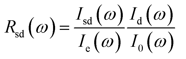
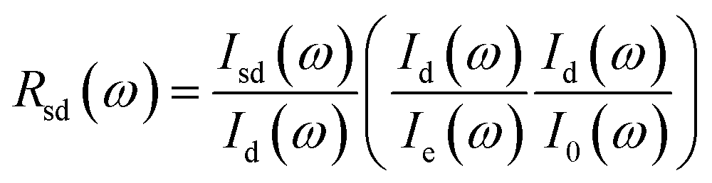
Because the direct contact between the sample and diamond culet, the reflectance from the sample–diamond interface (Rsd(ω)) can be calculated based on:38
 | (1) |
 | (2) |
In practice,  was measured and calculated at ambient pressure before samples loading and the ration of
  was fixed at 0.18. With the assumption of the pressure independent ratio of
 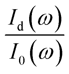 , the reflectance at each pressure can be determined accurately based on the ratio of
  measured at each corresponding pressure, multiply
 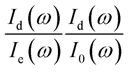 obtained at ambient pressure. The schematic geometry for the Rsd(ω) measurements in a diamond anvil cell is shown in Fig. 1a.
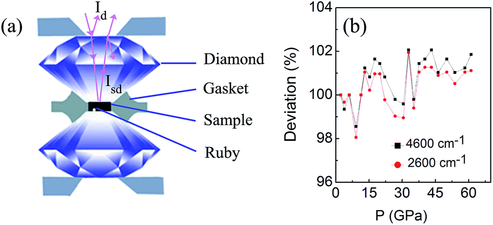 | ||
| Fig. 1 (a) The simplified optical geometry for the Rsd(ω) measurements in diamond anvil cell. (b) The percentage of the deviation calculated from Id(ω) at the point of 2600 cm−1 and 4600 cm−1, respectively. | ||
As a good estimation, the percentage of the deviation of the intensity reflected from the air–diamond interface was calculated as:
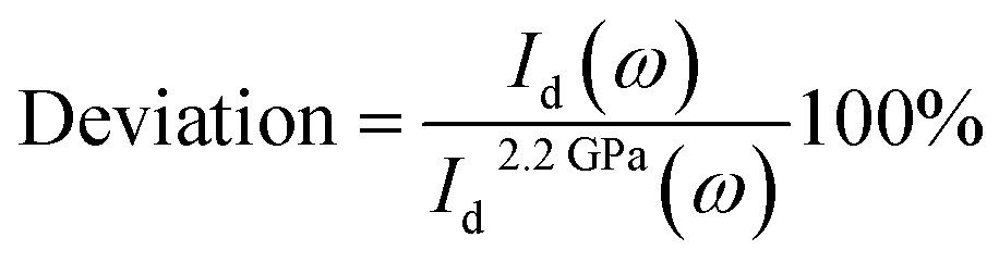 | (3) |
 of measured at each pressure is expected much smaller due to the shorter duration of the measurements.
Results and discussion
Fig. 2 shows the Rsd(ω) spectra for VO2 sample at selected pressures upon compression and their pressure dependence at the point of 1300 cm−1. The data between 1700 cm−1 and 2700 cm−1 were cut out from Rsd(ω) spectra due to the absorption of diamond. At 2.2 GPa, in contrast with that observed in early infrared high-pressure study on VO2, where only a steep rise in reflectivity was observed at low-frequency,23 we find two phonon peaks at about 650 cm−1 and 999 cm−1, which can be attributed to V = O vibrations as observed in the study on VO2 nanoparticles and film at ambient pressure.16,18,39 We suggest the differences mainly result from the amount of sample used in IR measurements. Instead of measuring the reflectivity of a 5 μm thick VO2 slab on KBr pellet as illustrated in reported high-pressure IR study, in this study, the high-pressure IR measurements were carried out using pure sample, which allows us to detect more details of Rsd(ω) spectra. At low pressure, Rsd(ω) gradually increase upon compressing. Above 11.4 GPa, Rsd(ω) starts to increase obviously and the phonon peak at about 999 cm−1 gradually broaden and weaken with increasing pressure, which is related to the structural transition from the M1 to the M′1 as observed in early study.22,29 Above 26.8 GPa, the Rsd(ω) shows a dramatic increase (the pressure dependence of R (1300 cm−1) shows a noticeable change in slope), and the phonon peak at about 999 cm−1 disappears, whereas a new phonon peak at about 800 cm−1 appears. These noticeable changes in Rsd(ω) may correspond with the start of structural transition from M′1 to the high-pressure X phase as observed early study.29 The slightly lower transition pressure from the M′1 to the X phase compared to that in early study may be results from the different pressure-transmitting media used in measurements. With further compressing, in Rsd(ω), the phonon peaks at about 650 cm−1 and 800 cm−1 gradually broaden and weaken, and finally disappears above 43.2 GPa (the phonon peaks indicated by the arrows in Fig. 2 come from measure environments). It worth noting that Rsd(ω) becomes nearly independent of the applied pressure at about Rsd(ω) = 0.55 for ω < 800 cm−1 above 43.2 GPa. As discussed in early study on MnO and MnTe2, the high value of reflectivity and their pressure independence suggest that the origin of the increase carrier is not pressure-dependent semimetallic band overlapping.23,30,37,40 Thus, the disappearance of the phonon peaks, and the high infrared reflectivity and it pressure insensitivity indicate that the VO2 samples above 43.2 GPa is metallic.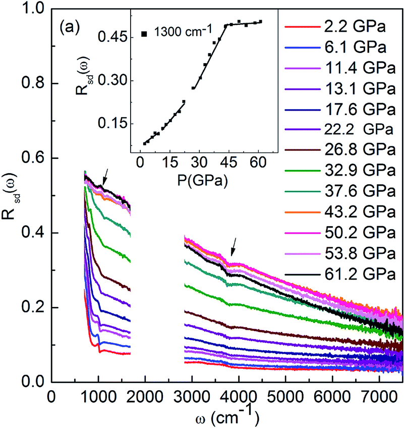 | ||
| Fig. 2 The reflectivity Rsd(ω) at selected pressure collected upon compression. Inset: pressure dependence of reflection at the point of 1300 cm−1. | ||
To further verify the PIM for monoclinic VO2, we presented the transmittance T(ω) spectra as a function of pressure in Fig. 3a. As illustrated above, the data below 1000 cm−1, between 1700 cm−1 and 2700 cm−1 were cut out from T(ω) spectra due to the absorption of diamond and the limit of the measuring range of our MIR detector, respectively. The bump at about 3500 cm−1 is result of the bad compensation of the diamond absorption.24 With increasing pressing, T(ω) gradually decreases up to 11.4 GPa. Upon further compressing, T(ω) starts to decrease more obviously. Compare with the data reported in early study (0–14), T(ω) show similar pressure dependence.23 When applied pressure increased to 20.9 GPa, T(ω) decreases to small values. And there almost no transmitted light in the whole spectrum range above 35.2 GPa (the enlarged spectra in the region of 800–1700 cm−1 is shown in the inset of Fig. 3a). These results indicate that the bandgap decreased to a value less than the minimum measured range 1000 cm−1 (0.12 eV). To follow the variation of bandgap under pressure, we also undertook estimation of the bandgap based on T(ω) spectra. Because of the presence of the bump at about 3500 cm−1 and the interference fringes in spectrum, it would yield relatively great errors in bandgap calculations using the methods employed in early study.6,7 Thus, we use the frequency (ωc), above which T(ω) = 0, to estimate the bandgap. The pressure dependence of ωc is shown in Fig. 3b. The ωc (P = 0) value is about 5270 cm−1 (0.65 eV), obtained by a rough linear extrapolation of the ωc values below 10 GPa in Fig. 3b, which is 0.05 eV larger than the bandgap value of VO2 at ambient pressure reported in early study.36 Therefore, the values of ωc (in eV) subtract 0.05 eV giving the corresponding approximate bandgap values at different pressure (Fig. 3c). Below 10.2 GPa, the band gap is weakly pressure dependent. On further increasing pressure, clear changes on slope at about 10.2 GPa and 25 GPa are observed, which could be related to structure transition from the M1 to M′1, and from M′1 to X phase, respectively. The band gap decrease to approximately 0.13 eV at about 29.6 GPa. Unfortunately we cannot calculate the smaller band gap values under higher pressure due to the limit of the measuring range of our MIR detector. We note that a rough linear extrapolation of the data gives a closed band gap at about 40–45 GPa, suggesting samples being metallic in this pressure range, which agree well with the results observed in our Rsd(ω) study.
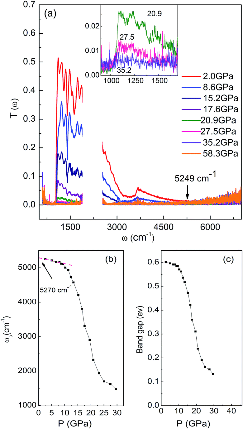 | ||
| Fig. 3 (a) MIR transmittance T(ω) of VO2 at selected pressures collected upon compression. (b) Pressure dependence of ωc. ωc represents the frequency at which T(ω) = 0, for example, P = 2.0 GPa, ωc = 5249 cm−1 (indicated by the arrows in (a)). (c) Pressure dependence of the band gap upon compression. Inset of (a): the enlarged spectrum in the region of 800–1700 cm−1. | ||
To have a better understand about this PIM process, we carried out high-pressure XRD measurements in characterizing the crystal structure transitions upon compression (Fig. 4). With increasing pressure, the expected the structure transition from M1 to M′1, and M′1 to the X phase were observed at about 13.1 GPa and 26.0 GPa, respectively. We note that the peak of the M′1 phase gradually decreases with increasing pressure above 26 GPa, whereas the intensity of the main M′1 phase diffraction line is almost the same as that of X phase at about 47.3 GPa, demonstrating that the M′1 phase is still the dominant phase at the critical pressure P = 43.2 GPa, where samples being metallic. These results indicate that the semiconductor M′1 transforms into a metallic M′1 phase. Goodenough reported a critical V–V separation value (2.93 ± 0.04 Å) for VO2, below which the V–V interaction is strong enough to delocalize the 3d electrons.12 At ambient pressure, a short (2.65 Å) and a long (3.12 Å) V–V separation alternating along a axis of M1 phase, leading to the insulating behavior. The pressure dependence of lattice parameters a, b, c and unit-cell volume are shown in Fig. 5. The a axis continuous decrease with pressure, whereas the b and c axes show noticeable changes in slope at about 13.1 GPa, indicating the anisotropy of M′1 phase. The unit-cell volume exhibits a regular continuous decrease under pressure, which can lead to a gradual decrease in atoms distance, thus, it is likely that the V–V separation become less than the critical value at about 43.2 GPa, resulting in the delocalization of the 3d electrons. These results suggest that the PIM in M′1 phase maybe mainly driven by electron–electron correlation, which agrees with the results reported by Baldini et al.25 and the results observed in our VO2 nanoparticles.41 Further, the structure transition from the M′1 to the X phase is completed above 59.0 GPa, where VO2 samples are metallic, revealing that the X phase is metallic.
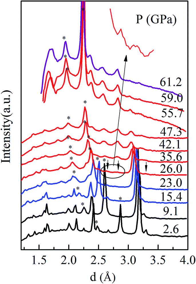 | ||
| Fig. 4 (a) XRD diffraction pattern of VO2 at selected pressures upon compression. Stars indicate diffraction peaks from Ar. | ||
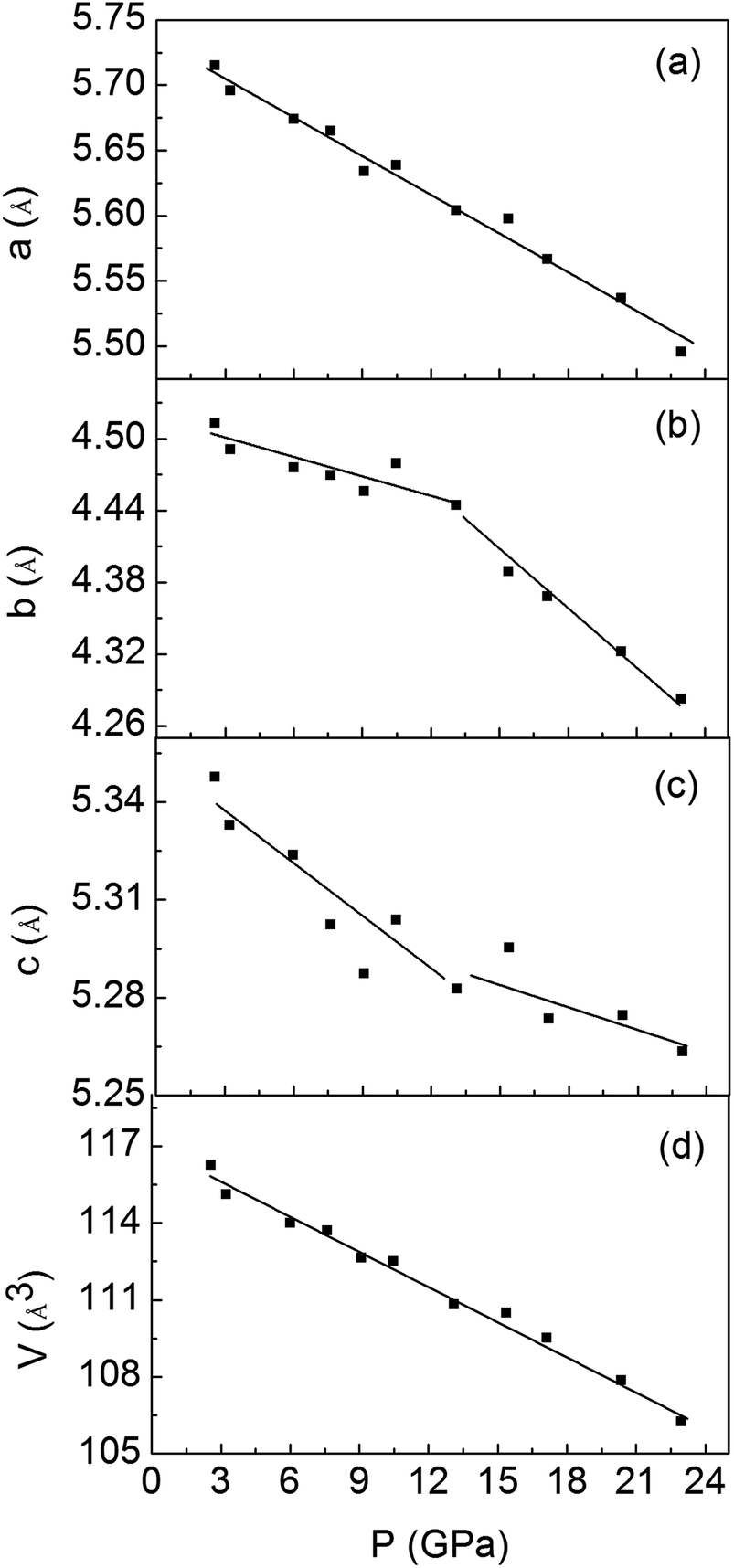 | ||
| Fig. 5 Pressure dependence of lattice parameters a, b, c and unit-cell volume [panels (a), (b), (c) and (d)] for VO2 samples. | ||
To gain further insight into the structure transition and metallization of VO2 (M1) under pressure, we carried out high pressure Raman measurements up to 64.7 GPa shown in Fig. 6a. The spectrum at 3.7 GPa is in full agreement with previous Raman data on VO2 in M1 phase.23 The Raman mode frequencies are plotted as a function of pressure in Fig. 6b. Upon compression to 12.9 GPa, a slight change in slope was observed and two weak Raman peaks disappear, suggesting a structural transition from M1 phase to M′1 phase occurs. These results compare well with our XRD study and early reports on VO2 samples.23,29 It is reported that the Raman modes A and B are associated with the paring and tilting motions of V-ions motion in the dimerized chins.23,24,29 When pressure increased above 27.0 GPa, the Raman modes A and B gradually broaden and weaken, moreover, the Raman modes B displays a sharp slope change (Fig. 6b), suggesting the onset of the structure transition from M′1 to the X phase. The most important evidence is that the Raman modes A and B are still well distinguished up to about 50.5 GPa, demonstrating that the V–V dimers exist up to this pressure. Recently, M. Baldini et al. found that the V–V dimers is not suppressed in M′1 phase by means of high pressure atomic pair distribution function measurements up to 22 GPa, and pointed that the suppression of Peierls distortion is not correlated with the change of the electronic properties within the pressure range under investigation.25 In our Raman study, it is clearly shown that the V–V dimers exist up to 50.5 GPa, above the pressure (43 GPa) where the PIM transition occurs, thus, demonstrating that the PIM in M′1 phase is not related to the suppression of Peierls distortion.
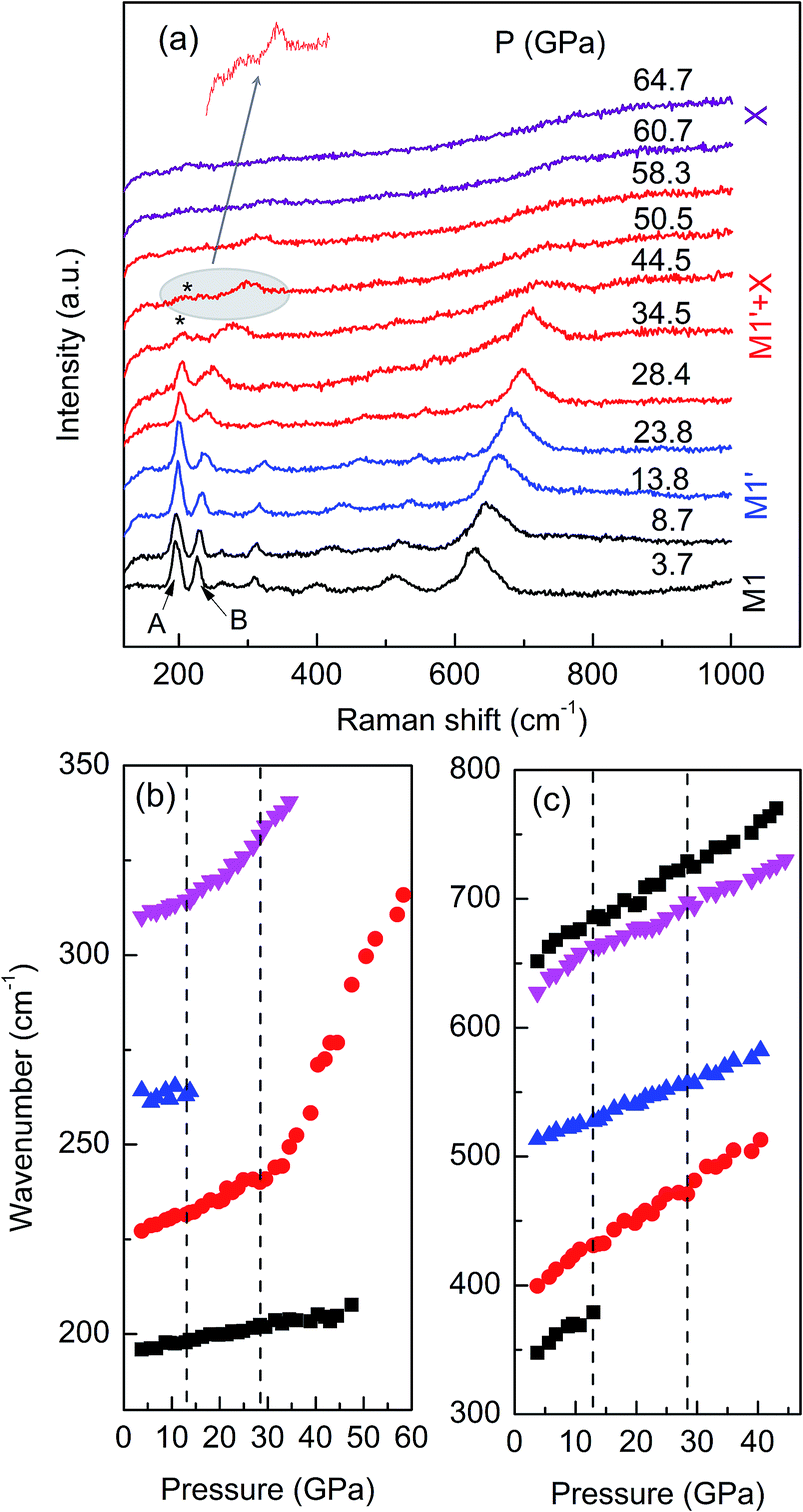 | ||
| Fig. 6 (a) Raman spectra of VO2 at selected pressures upon compression. (b and c) Pressure dependence of the frequency of the observed Raman modes upon compression. | ||
Moreover, when the pressure increased above 58.3 GPa, all Raman modes, including the A and B, disappear, suggesting the suppression of Peierls distortion. It is shown in our XRD study that all the structure transition from M′1 phase into the high pressure X phase is completed at about 59 GPa, thus, we can guess that the Peierls distortion is suppressed in X phase and the metallization in X phase is mainly related to structure transition.
Conclusions
In summary, the insulator–metal and metal–insulator transition processes of VO2 are observed by IR measurements. Upon compression, VO2 samples transform from insulator monoclinic M1 into semiconductor monoclinic M′1 at about 11.4 GPa. With further compressing, the structure transition from M′1 to metallic X phase starts at about 26.8 GPa. When pressure increased to 43.2 GPa, only part of VO2 sample in M′1 transforms into metallic X phase, whereas the rest of samples in M′1 become metallic. In addition, all the samples transformed into metallic X above 59.0 GPa. Present results demonstrate that the PIM in the M′1 phase mainly driven by electron–electron correlation, whereas, the PIM from the insulating M′1 phase to the X phase is related to the structural transition.Acknowledgements
This work was financially supported by the National Basic Research Program of China (2011CB808200), NSFC (51320105007, 11374120, 11634004, 51632002, and 51572108), Program for Changjiang Scholars and Innovative Research Team in University (No. IRT_15R23), the visiting scholar project funded by China Scholarship Council, and the Cheung Kong Scholars Programme of China.References
- S. H. Reichman, J. E. Kosin and J. F. Meyerink, US Pat. 6,053,993[P], 25 April 2000.
- M. Aureliano and D. C. Crans, J. Inorg. Biochem., 2009, 103, 536–546 CrossRef CAS PubMed.
- E. Kioseoglou, S. Petanidis and C. Gabriel, et al., Coord. Chem. Rev., 2015, 301, 87–105 CrossRef.
- S. Zhang, I. S. Kim and L. J. Lauhon, Nano Lett., 2011, 11, 1443–1447 CrossRef CAS PubMed.
- K. W. Lee, J. J. Kweon and C. E. Lee, et al., Appl. Phys. Lett., 2010, 96, 243111 CrossRef.
- F. J. Morin, Phys. Rev. Lett., 1959, 3, 34–36 CrossRef CAS.
- M. Marezio, D. B. McWhan, J. P. Remeika and P. D. Dernier, Phys. Rev. B: Solid State, 1972, 5, 2541–2551 CrossRef.
- J. P. Pouget, H. Launois, J. P. D'Haenens, P. Merenda and T. M. Rice, Phys. Rev. Lett., 1975, 35, 873–875 CrossRef CAS.
- A. Zylbersztejn and N. F. Mott, Phys. Rev. B: Solid State, 1975, 11, 4383–4395 CrossRef CAS.
- R. Lopez, T. E. Haynes, L. A. Boatner, L. C. Feldman and R. F. Haglund, Phys. Rev. B: Condens. Matter Mater. Phys., 2002, 65, 224113 CrossRef.
- H. T. Kim, Y. W. Lee, B. J. Kim, B. G. Chae, S. J. Yun, K. Y. Kang, K. J. Han, K. J. Yee and Y. S. Lim, Phys. Rev. Lett., 2006, 97, 266401 CrossRef PubMed.
- J. B. Goodenough, Annu. Rev. Mater. Sci., 1971, 1, 101–138 CrossRef CAS.
- D. Okuyama, K. Shibuya and R. Kumai, et al., Phys. Rev. B: Condens. Matter Mater. Phys., 2015, 91, 064101 CrossRef.
- S. Biermann, A. Poteryaev, A. I. Lichtenstein and A. Georges, Phys. Rev. Lett., 2005, 94, 026404 CrossRef CAS PubMed.
- A. X. Gray, J. Jeong and N. P. Aetukuri, et al., Phys. Rev. Lett., 2016, 116, 116403 CrossRef CAS PubMed.
- H. S. Choi, J. S. Ahn, J. H. Jung and T. W. Noh, Phys. Rev. B: Condens. Matter Mater. Phys., 1996, 54, 4621–4628 CrossRef CAS.
- J. Yang and Z. Xu, et al., Appl. Energy, 2015, 159, 502–508 CrossRef CAS.
- K. W. Lee, J. J. Kweon, C. E. Lee, A. Gedanken and R. Ganesan, Appl. Phys. Lett., 2010, 96, 243111 CrossRef.
- L. Bai, Q. Li, S. A. Corr, M. Pravica, C. Chen, Y. Zhao, S. V. Sinogeikin, Y. Meng, C. Park and G. Shen, Phys. Rev. B: Condens. Matter Mater. Phys., 2015, 92, 134106 CrossRef.
- Y. Ding, C. C. Chen, Q. Zeng, H. S. Kim, M. J. Han, M. Balasubramanian, R. Gordon, F. Li, L. Bai, D. Popov, S. M. Heald, T. Gog, H. K. Mao and M. van Veenendaal, Phys. Rev. Lett., 2014, 112, 056401 CrossRef PubMed.
- C.-C. Chen, A. Herhold, C. Johnson and A. Alivisatos, Science, 1997, 276, 398–401 CrossRef CAS PubMed.
- M. Mitrano, B. Maroni, C. Marini, M. Hanfland, B. Joseph, P. Postorino and L. Malavasi, Phys. Rev. B: Condens. Matter Mater. Phys., 2012, 85, 184108 CrossRef.
- E. Arcangeletti, L. Baldassarre, D. Di Castro, S. Lupi, L. Malavasi, C. Marini, A. Perucchi and P. Postorino, Phys. Rev. Lett., 2007, 98, 196406 CrossRef CAS PubMed.
- C. Marini, E. Arcangeletti, D. Di Castro, L. Baldassare, A. Perucchi, S. Lupi, L. Malavasi, L. Boeri, E. Pomjakushina, K. Conder and P. Postorino, Phys. Rev. B: Condens. Matter Mater. Phys., 2008, 77, 235111 CrossRef.
- M. Baldini, P. Postorino, L. Malavasi, C. Marini, K. W. Chapman and H.-K. Mao, Phys. Rev. B, 2016, 93, 245137 CrossRef.
- C. H. Neuman, A. W. Lawson and R. F. Brown, J. Chem. Phys., 1964, 41, 1591–1595 CrossRef CAS.
- C. N. Berglund and A. Jayaraman, Phys. Rev., 1969, 185, 1034–1039 CrossRef CAS.
- X. Zhang, J. Zhang, F. Ke, G. Li, Y. Ma, X. Liu, C. Liu, Y. Han, Y. Ma and C. Gao, RSC Adv., 2015, 5, 54843–54847 RSC.
- L. Bai, Q. Li, S. A. Corr, Y. Meng, C. Park, S. V. Sinogeikin, C. Ko, J. Wu and G. Shen, Phys. Rev. B: Condens. Matter Mater. Phys., 2015, 91, 104110 CrossRef.
- Y. Mita, D. Izaki, M. Kobayashi and S. Endo, Phys. Rev. B: Condens. Matter Mater. Phys., 2005, 71, 100110 CrossRef.
- M. M. Qazilbash, M. Brehm, B.-G. Chae, P. C. Ho, G. O. Andreev, B.-J. Kim, S. J. Yun, A. V. Balatsky, M. B. Maple, F. Keilmann, H.-T. Kim and D. N. Basov, Science, 2007, 318, 1750–1753 CrossRef CAS PubMed.
- Y. Sun, S. Jiang, W. Bi, R. Long, X. Tan, C. Wu, S. Wei and Y. Xie, Nanoscale, 2011, 3, 4394–4401 RSC.
- W. T. Liu, J. Cao, W. Fan, Z. Hao, M. C. Martin, Y. R. Shen, J. Wu and F. Wang, Nano Lett., 2011, 11, 466–470 CrossRef CAS PubMed.
- X. J. Chen, V. V. Struzhkin, Y. Song, A. F. Goncharov, M. Ahart, Z. Liu, H. K. Mao and R. J. Hemley, Proc. Natl. Acad. Sci. U. S. A., 2008, 105, 20–23 CrossRef CAS PubMed.
- L. Baldassarre, A. Perucchi, E. Arcangeletti, D. Nicoletti, D. Di Castro, P. Postorino, V. A. Sidorov and S. Lupi, Phys. Rev. B: Condens. Matter Mater. Phys., 2007, 75, 245108 CrossRef.
- H. W. Verleur, A. S. Barker and C. N. Berglund, Phys. Rev., 1968, 172, 788–798 CrossRef CAS.
- B. Cheng, Q. Li, H. Zhang, R. Liu, B. Liu, Z. Yao, T. Cui, J. Liu, Z. Liu, B. Sundqvist and B. Liu, Phys. Rev. B, 2016, 93, 184109 CrossRef.
- C. T. Seagle, D. L. Heinz, Z. Liu and R. J. Hemley, Appl. Opt., 2009, 48, 545–552 CrossRef CAS PubMed.
- M. M. Qazilbash, M. Brehm, G. O. Andreev, A. Frenzel, P. C. Ho, B.-G. Chae, B.-J. Kim, S. J. Yun, H.-T. Kim, A. V. Balatsky, O. G. Shpyrko, M. B. Maple, F. Keilmann and D. N. Basov, Phys. Rev. B: Condens. Matter Mater. Phys., 2009, 79, 075107 CrossRef.
- Y. Mita, Y. Ishida and M. Kobayashi, Acta Phys. Pol., A, 2008, 113, 617–620 CrossRef CAS.
- Q. Li, H. Zhang, C. Lin, F. Tian, J. S. Smith, C. Park, B. Liu and G. Shen, Pressure-induced phase transitions and insulator–metal transitions in VO2 nanoparticles, J. Appl. Phys. Search PubMed , (unpublished).
| This journal is © The Royal Society of Chemistry 2016 |