
Improved efficiency of solution-processed bulk-heterojunction organic solar cells and planar-heterojunction perovskite solar cells with efficient hole-extracting Si nanocrystals†
Hanbin Jeong‡
a,
Hansol Kim‡a,
Won-Il Song‡b,
Kyung-Hoon Yoo‡b,
Jason Rama‡c and
Jae Kwan Lee‡*a
aDepartment of Chemistry Education/Carbon Materials, Chosun University, Gwangju, 501-759, Republic of Korea. E-mail: Chemedujk@chosun.ac.kr; Tel: +82 62 230 7319
bAdvanced Convergent Technology R&D, Korea Institute of Industrial Technology, Gyunggi, 426-910, Korea
cMeliorum Technologies, Inc., Rochester, New York 14607, USA
First published on 28th October 2016
Abstract
We demonstrate the efficiency enhancement and efficient hole extraction achieved by undoped Si nanocrystals (NCs) and p-type Si (p-Si) NCs in solution-processed bulk-heterojunction (BHJ) organic solar cells (OSCs) and planar-heterojunction (PHJ) perovskite solar cells (PrSCs). We observed that the surface coverage of Si–NCs on the substrate significantly affected the photovoltaic performance of the BHJ OSCs and PHJ PrSCs. The undoped Si NCs and p-Si NCs enhanced the power conversion efficiencies (PCEs) of the BHJ OSCs by ∼6% and ∼11%, respectively, and those of PHJ PrSCs by ∼22% and ∼23%, correspondingly, compared with the PCEs of devices without Si NCs. The p-Si NCs had a highest occupied molecular orbital (HOMO) energy level ∼0.16 eV higher than that of undoped Si NCs and showed better balances with the HOMO energy levels of the PTB7-Th and MAPbI3 perovskite materials, achieving an increase in the hole mobility of the BHJ system, and thus demonstrating their key role as hole-extracting materials.
Introduction
Solution-processed solar cells have attracted great interest because of their easy and inexpensive manufacturing processes, including versatile methods such as inkjet, doctor-blade, and roll-to-roll printing.1,2 Recently, considerable efforts have been focused on achieving competitive power conversion efficiencies (PCEs) competitive with those of conventional silicon-based solar cells. As a promising alternative, solution-processed organic solar cells (OSCs) have exhibited excellent PCEs of ∼10% for the low-bandgap poly(thieno[3,4-b]thiophene-alt-benzodithiophene) based semiconducting polymer (PTB7-Th) and [6,6]-phenyl-C(61 or 71)-butyric acid methyl ester (PC(61 or 71)BM) bulk-heterojunctions (BHJs).3 Very recently, solution-processable organometal halide perovskite solar cells (PrSCs), especially those containing (CH3NH3)PbX3 [MAPbX3, (X = Cl, Br, I)] have also received considerable attention because they have exhibited exceptional PCEs of over 15%.4–6 Specifically, p–i–n type PrSCs are often fabricated using planar heterojunction (PHJ) bilayer structures of perovskite materials and PCBM.7 Because these BHJ OSCs and PHJ PrSCs have quite similar device configuration comprising of indium tin oxide (ITO)/poly(3,4-ethylenedioxythiophene):poly-(styrenesulfonate) (PEDOT:PSS)/donor:acceptor/Al,8 various strategies have been adopted to obtain high PCEs. Examples include the development of high-performance semiconducting polymer materials or perovskite materials,9–12 effective functions with surface plasmon resonances,13,14 charge transport,15,16 and charge extraction17,18 in device structures, and morphological engineering by thermal annealing,19,20 solvent-casting,5,21 or processing additives.22,23Among these approaches, efficient charge-extraction materials, which can effectively suppress carrier recombination or trapping, have been often employed to achieve enhanced PCEs.24 This is because the extraction efficiency for charge carriers separated from excitons in interfaces of donor and acceptor has been known to be one of the influential factors affecting the PCEs of these solution-processed solar cells. In particular, wide-bandgap inorganic nanocrystals (NCs) such as TiO2 (or ZnO) and MoO3 have exhibited excellent electron-extracting and hole-extracting features, respectively, in BHJ OSCs and PHJ PrSCs.25–27 Additionally, inorganic semiconductor NCs such as CdS, CdSe, and PbS, could also be utilized in hybrid solar cells (HSCs) with organic semiconductors because their optical and electronic properties can be tailored through size-dependent bandgap engineering.28,29 However, owing to the toxicity of these materials, HSCs fabricated with polymer donors using environmentally benign Si NCs as the electron acceptor have been recently reported but they also suffer from lower PCEs than those of BHJ OSCs with PCBM.30,31 Nonetheless, their highly desirable optical and electronic properties depend on their nanometer-scale size and the carrier concentration induced by doping,32 which may make their integration into HSCs challenge.
On the other hand, very recently, we reported an efficiency improvement in OSCs with a ternary BHJ (TBHJ) configuration consisting of the nanostructured perovskite-low bandgap polymer-PCBM.33 A TBHJ device, which was constructed with a semiconducting polymer-PCBM BHJ integrated on perovskite nanostructures exhibited better photovoltaic performance than a BHJ device without perovskite materials because perovskite materials play a key role as electron and hole conductors and photosensitizers.4–7 Based on these results, we attempted for the first time to utilize Si NCs as hole extraction materials (HEMs) in solution processed BHJ OSCs using a TBHJ device architecture because there is little research on the incorporation of Si NCs in HSCs as HEMs. Additionally, we speculated that this approach can be employed in PHJ PrSCs fabricated using bilayer structures of perovskite materials and PCBM on ITO/PEDOT:PSS substrates.
Herein, we report the efficiency enhancement of solution-processed BHJ OSCs and PHJ PrSCs using hole-extracting Si NCs. Additionally, we compared the HEM efficacy of undoped Si NCs and p-type Si NCs in these devices. The examined solution-processed BHJ OSCs and PHJ PrSCs had device configurations of ITO/PEDOT:PSS/PTB7-Th:PC71BM/Al and ITO/PEDOT:PSS/MAPbI3/PC61BM/Al, respectively, and the Si NC HEMs were spin-cast on an ITO/PEDOT:PSS substrate. Fig. 1 shows the device architectures of the solution-processed BHJ OSCs and PHJ PrSCs, which were fabricated with Si NC HEMs cast on an ITO/PEDOT:PSS substrate. The sparse coverage of the Si NCs on the ITO/PEDOT:PSS substrate was readily demonstrated by varying the concentration of Si NCs dispersed in a chlorobenzene (CB) solvent. Notably, outstanding performances were observed in the hybrid devices constructed with BHJ (or PHJ) layers on PEDOT:PSS/Si NCs and the Si NCs obviously played a key role for the easy extraction of hole carriers separated from excitons in interfaces of the donors and the PCBM. Specifically, the PCEs of the BHJ OSCs and PHJ PrSCs were enhanced by ∼11% and ∼23%, respectively, compared with those of the corresponding devices without Si NC HEMs. Furthermore, the highest occupied molecular orbital (HOMO) energy level of p-Si NCs is ∼0.16 eV higher than that of undoped Si NCs. Therefore, the p-Si NCs showed better balances between the HOMO energy levels of PTB7-Th and MAPbI3 perovskite materials, resulting in optimal PCEs in both BHJ OSCs and PHJ PrSCs.
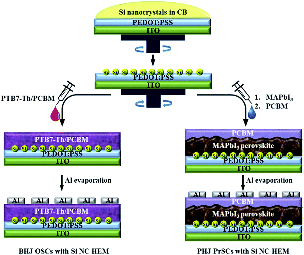 | ||
| Fig. 1 Schematic descriptions for fabrication of solution-processed BHJ OSCs and PHJ PrSCs device structures with Si NC HEMs. | ||
Experimental
Materials
The PbI2 was purchased from Aldrich and CH3NH3I was prepared according to a previously reported method.8 All solvents were purchased from Sigma-Aldrich, TCI, and Alfa Aesar and were purified using the appropriate methods. The MAPbI3 precursor solution was prepared in a nitrogen atmosphere. The PTB7-Th and PCBM were obtained from 1-Materials and Nano-C, respectively. B-doped and undoped polycrystalline silicon wafers were purchased from University Wafer.Preparation of Si NCs
The Si NCs were produced using a modified electrochemical etching process,34 using a wafer feedstock that was pulverized while being slowly dipped into a solution of HF and H2O2. The B-doped and undoped polycrystalline silicon wafers were used to provide p-Si NCs and undoped Si NCs, respectively. These wafers were placed in a bath of n-hexadecane and ultrasonicated to form a suspension of small Si particles, which were transferred from the n-hexadecane to CB before use.Measurements and instruments
Transmittance spectra were recorded using a Perkin-Elmer Lambda 2S ultraviolet-visible spectrometer. The surface morphologies were imaged using a field emission scanning electron microscope (FESEM, Nova nanoSEM 450, FEI, Netherlands) and a high-resolution transmission electron microscope (HRTEM, G2 F20, FEI Tecnai, Netherlands). The HOMO of the materials was estimated from their ionization potential, which was measured using ultraviolet photoelectron spectroscopy (UPS) in air (surface analyzer, AC2, Riken Keiki, Co., Ltd., Japan). The solar cell efficiencies were determined under simulated 100 mW cm−2 AM 1.5G irradiation from a Xe arc lamp with an AM 1.5 global filter. The simulator irradiance was characterized using a calibrated spectrometer and the illumination intensity was set using a silicon diode with an integrated KG1 optical filter certified by the National Renewable Energy Laboratory. The spectral mismatch factors were calculated to be lower than 5% for all devices. The short circuit currents were also observed to be within 5% of the values calculated using the integrated external quantum efficiency (EQE) spectra and the solar spectrum. The applied potential and cell currents were measured using a Keithley 2400 digital source meter. The current density–voltage (J–V) curves were measured at a voltage settling time of 100 ms. The EQEs were measured by under filling the device area using a reflective microscope objective to focus the light output from a 75 W Xe lamp, a monochromator, and an optical chopper. The photocurrent was measured using a lock-in amplifier, the absolute photon flux was determined using a calibrated silicon photodiode and was recorded for 5 s per point (80 points) between 350–1100 nm.Device fabrication
The ITO-coated glass substrates were cleaned with detergent, ultrasonicated in acetone and isopropyl alcohol, and dried overnight in an oven. An aqueous solution of PEDOT:PSS (Heraeus, Clevios P VP AI 4083) was spin-cast onto the ITO substrates to form a film ∼35 nm in thickness. The substrate was dried in air at 140 °C for 10 min and was transferred into a glove box for spin-casting of the Si NC solution. The Si NC solution was prepared in CB at 0.024, 0.034, 0.057, 0.171, and 0.854 mg ml−1 and was uniformly dispersed by sonication for 10 min before use. These were spin-cast at 2000 rpm for 60 s and dried at 60 °C for 10 min. A BHJ active layer and a PHJ bilayer were deposited on the ITO/PEDOT:PSS/Si NC substrate for OSCs and PrSCs, respectively, as follows: for the OSC, a PTB7-Th:PC71BM BHJ blend solution (weight ratio, 1![[thin space (1/6-em)]](https://www.rsc.org/images/entities/char_2009.gif) :1.5) with diiodooctane additive (2 vol%) was spin-cast at 2000 rpm and was subsequently heat-treated at 80 °C for 10 min. For the PrSCs, a MAPbI3 precursor solution was prepared using PbI2 and CH3NH3I (molar ratio 1:1) in dimethylformamide at 60 wt% and stirred at 60 °C for 12 h. The MAPbI3 perovskite films were produced by spin-casting at 5000 rpm for 30 s using the MAPbI3 precursor solution and by dripping of CB; they were then dried on a hot plate at 100 °C for 10 min. The PC61BM solution was spin-cast on top of the MAPbI3 layer and the process was followed by heat-treatment at 80 °C for 10 min. Finally, an Al metal electrode of thickness ∼100 nm was deposited on top of the PTB7-Th:PC71BM BHJ film and MAPbI3/PC61BM PHJ film at low pressure (below 10−6 Torr).
:1.5) with diiodooctane additive (2 vol%) was spin-cast at 2000 rpm and was subsequently heat-treated at 80 °C for 10 min. For the PrSCs, a MAPbI3 precursor solution was prepared using PbI2 and CH3NH3I (molar ratio 1:1) in dimethylformamide at 60 wt% and stirred at 60 °C for 12 h. The MAPbI3 perovskite films were produced by spin-casting at 5000 rpm for 30 s using the MAPbI3 precursor solution and by dripping of CB; they were then dried on a hot plate at 100 °C for 10 min. The PC61BM solution was spin-cast on top of the MAPbI3 layer and the process was followed by heat-treatment at 80 °C for 10 min. Finally, an Al metal electrode of thickness ∼100 nm was deposited on top of the PTB7-Th:PC71BM BHJ film and MAPbI3/PC61BM PHJ film at low pressure (below 10−6 Torr).
Results and discussion
Fig. 2 shows (a) HRTEM images (inset) of the synthesized Si NCs and the ultraviolet photoelectron spectra of the p-Si NCs and undoped Si NCs and (b) the HOMO energy levels of these Si NCs. The HOMO values were estimated from the ionization potentials, which were obtained using UPS analysis, and compared with those of PTB7-Th and MAPbI3 materials (see Fig. S1 in the ESI†). The Si NCs were prepared by a modified electrochemical etching method,34 using a wafer feedstock that was pulverized while being slowly dipped into a solution of HF and H2O2. The particles were produced by Si:H passivation. Additionally, these Si nanoparticles had polycrystalline morphologies because they were fabricated using polycrystalline silicon wafer resources. As shown in Fig. 2a (inset), the small particulate Si NCs had an average size of ∼5 nm, which was determined by dynamic light scattering analysis as shown in Fig. S2,† and appeared to be agglomerated to 50–100 nm because of their high surface energy.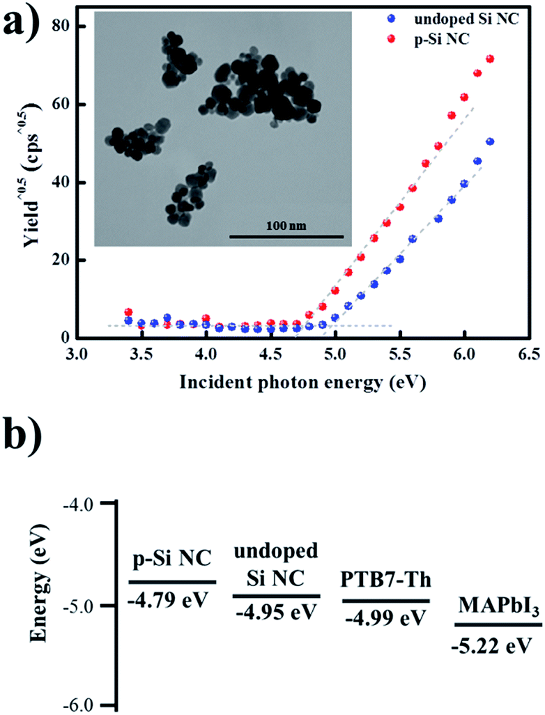 | ||
| Fig. 2 (a) HRTEM images (inset) of synthesized Si NCs (∼5 nm) and ultraviolet photoelectron spectra of p-type Si NCs and undoped Si NCs and (b) HOMO energy levels of these Si NCs, PTB7-Th, and MAPbI3 materials. | ||
In this work, we used two types (p-type and undoped) Si NCs to evaluate their efficacy as HEM materials for solution-processed BHJ OSCs and PHJ PrSCs. Although Si NCs are often prepared with various bottom-up synthesis techniques, fabricating Si NCs whilst retaining Si:H surface passivation is very difficult. However, the electrochemical etching process used in this work readily provided p-Si NCs and undoped Si NCs from commercially available B-doped and undoped polycrystalline silicon wafers, respectively. The light emissions of these Si NCs were examined using their photoluminescence spectra (Fig. S3†). Because these particles were not smaller than the typical Bohr radius of the exciton of silicon, they did not exhibit a discrete density of states; hence, no size-dependent quantum confinement effects were expected to occur.35 However, the luminescence in here is designed to result from the surface states of the particles. As shown in Fig. 2b, the HOMO of p-Si NCs is −4.79 eV, which is ∼0.16 eV higher than the value (−4.95 eV) of undoped Si NC. The HOMOs of PTB7-Th and MAPbI3 materials were obtained as −4.99 eV and −5.22 eV, respectively, under the same measuring conditions.36 These results indicate that the HOMO value of p-Si NCs could have a better balance with those of PTB7-Th and MAPbI3 perovskite materials than undoped Si NCs, indicating a better performance of BHJ OSCs and PHJ PrSCs as HEMs.
Fig. 3 presents FESEM surface images of Si NCs spin-cast on the ITO/PEDOT:PSS substrates for various Si NCs concentrations (0.024, 0.034, 0.057, 0.171, and 0.854 mg ml−1) in CB. As shown in Fig. 3, the Si NCs cast on the ITO/PEDOT:PSS substrates exhibited a sparser surface coverage at low concentrations and a dense surface coverage for concentration above 0.8 mg ml−1; however, they exhibited non-uniform film morphologies for Si NC agglomerates of 50–100 nm as shown in Fig. 2a (inset). Based on these results, we employed the discussed PEDOT:PSS/Si NCs HEM layer in both the OSCs and the PrSCs fabricated from the PTB7-Th:PC71BM BHJ film and MAPbI3/PC61BM PHJ film, respectively.
 | ||
| Fig. 3 FESEM surface images of Si NCs spin-cast on the ITO/PEDOT:PSS substrates for various Si NCs concentrations ((a) 0, (b) 0.024, (c) 0.034, (d) 0.057, (e) 0.171, and (f) 0.854 mg ml−1) in CB. | ||
Fig. 4 shows the photovoltaic performances of these BHJ OSC and PHJ PrSC devices with PEDOT:PSS/Si NC HEM layers fabricated at various concentrations (0.024, 0.034, 0.057, 0.171, and 0.854 mg ml−1) of p-Si NCs in CB solvent; these are compared with the performances of the corresponding devices without Si NCs. The displayed values were determined from the average of individual hybrid solar cells fabricated under conditions optimized for the construction of BHJ OSCs and PHJ PrSCs without Si NCs materials (see Table S1 in the ESI†). The surface coverage on the substrate can significantly affect the photovoltaic performance of the BHJ OSCs and PHJ PrSCs as shown in Fig. 4. Additionally, both the BHJ OSCs and the PHJ PrSCs with PEDOT:PSS/p-Si NC HEM layers that were fabricated using a p-Si NC solution of 0.034 mg ml−1 exhibited the most improved photovoltaic performance compared to the devices without Si NCs. The results indicate that the increased PCE of the BHJ OSCs and PHJ PrSCs with PEDOT:PSS/p-Si NC HEM layers was obviously induced by their significantly enhanced photocurrents. However, the BHJ OSC and PHJ PrSC devices fabricated with solution concentrations higher than 0.170 mg ml−1 exhibited some degraded photovoltaic performances owing to short-circuit current density (Jsc) losses and both the open-circuit voltage (Voc) and fill factor (FF), respectively.
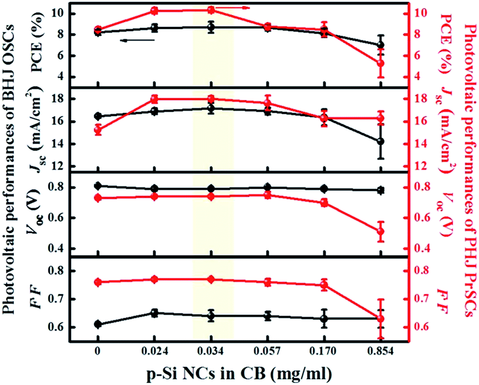 | ||
| Fig. 4 Photovoltaic performances of these BHJ OSC (black) and PHJ PrSC (red) devices with PEDOT:PSS/p-Si NC HEM layers fabricated at various concentrations (0, 0.024, 0.034, 0.057, 0.171, and 0.854 mg ml−1) of Si NCs in CB solvent. | ||
Next, we prepared two types (p-type and undoped) Si NCs and utilized them in solution-processed BHJ OSCs and PHJ PrSCs fabricated from the PTB7-Th:PC71BM BHJ film and MAPbI3/PC61BM PHJ films to evaluate the Si NC HEM efficacy. Fig. 5 presents the J–V curves of BHJ OSCs and PHJ PrSCs fabricated under optimized processing conditions with (p-type and undoped) Si NCs (0.034 mg ml−1) deposited on PEDOT:PSS substrates; the curves were measured under AM 1.5 irradiation (100 mW cm−2) and are compared those (black) of devices without Si NCs. The corresponding values are summarized in Table 1. As shown in Fig. 5 and Table 1, the BHJ OSC devices fabricated with undoped Si NCs showed a ∼6% PCE enhancement compared with the BHJ OSCs without Si NC HEMs, with a PCE (best/average) of 8.85/8.31% with Jsc = 17.3/16.9 mA cm−2, Voc = 0.80/0.79 V, and FF = 0.64/0.63. The devices with p-Si NCs exhibited PCEs enhanced by ∼11%, with PCE = 9.25/8.70% with Jsc = 17.8/17.2 mA cm−2, Voc = 0.80/0.79 V, and FF = 0.66/0.64. The corresponding values of the BHJ OSCs without Si NC HEMs were PCE = 8.35/8.21% with Jsc = 16.6/16.5 mA cm−2, Voc = 0.82/0.81 V, and FF = 0.62/0.61. Moreover, the PHJ PrSC devices fabricated with undoped Si NCs and p-Si NCs exhibited enhanced PCEs by ∼22% and ∼23%; for the former, we measured a PCE (best/average) of 10.52/10.33% with Jsc = 18.2/18.0 mA cm−2, Voc = 0.75/0.74 V, and FF = 0.78/0.77; for the latter, PCE = 10.49/10.17% with Jsc = 17.7/17.3 mA cm−2, Voc = 0.74/0.73 V, and FF = 0.80/0.79. The corresponding values determined for the PHJ PrSCs without Si NC HEMs were PCE = 8.59/8.47% with Jsc = 15.7/15.2 mA cm−2, Voc = 0.74/0.73 V, and FF = 0.77/0.76. From these results, the OSC devices fabricated with PTB7-Th:PC71BM BHJ film cast on PEDOT:PSS/p-Si NCs obviously presented better photovoltaic performances than those with PEDOT:PSS/undoped Si NCs, whereas the PrSC devices fabricated with MAPbI3/PC61BM PHJ film showed similar HEM efficacy for both p-Si NCs an undoped Si NCs. This indicates a significant enhancement of the photovoltaic performances of the PHJ PrSC devices compared with those of BHJ OSCs with Si NC HEMs. This behavior might originate from the balances of the HOMO values of the p-Si NCs and undoped Si NCs with those of PTB7-Th and MAPbI3 perovskite materials as shown in Fig. 2b.
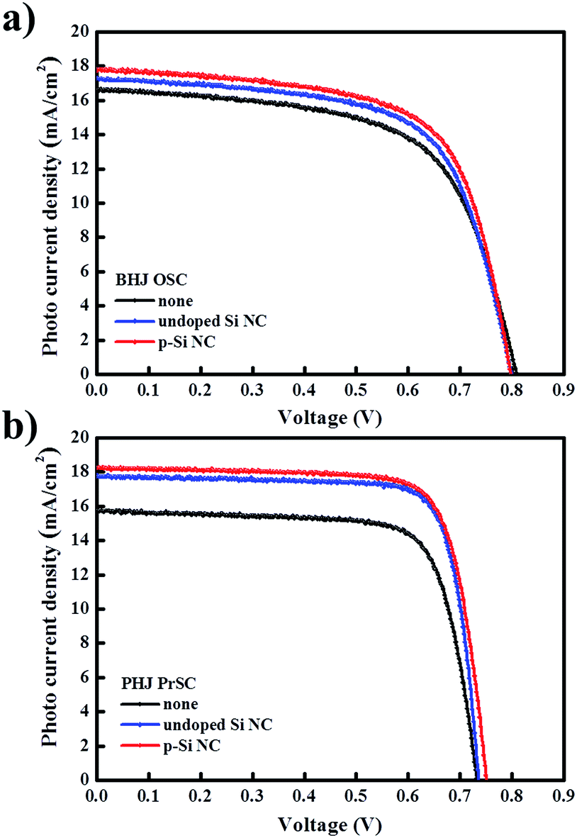 | ||
| Fig. 5 (a) Distribution J–V curves under AM 1.5 irradiation (100 mW cm−2) for (a) BHJ OSCs and (b) PHJ PrSCs fabricated under optimized processing conditions with (p-type (red) and undoped (blue)) Si NCs (0.034 mg ml−1) deposited on PEDOT:PSS substrate and compared those (black) without Si NCs. | ||
| Device | Si NCs | Jsc best/ave (mA cm−2) | Voc best/ave (V) | FFbest/ave | ηbest/ave (%) |
|---|---|---|---|---|---|
| a The performances are determined under simulated 100 mW cm−2 AM 1.5 illumination. The light intensity using calibrated standard silicon solar cells with a proactive window made from KG5 filter glass traced to the NREL. The active area of device is 4.5 mm2. | |||||
| BHJ OSC | None | 16.6/16.5 | 0.82/0.81 | 0.62/0.61 | 8.35/8.21 |
| Undoped | 17.3/16.9 | 0.80/0.79 | 0.64/0.63 | 8.85/8.31 | |
| p-Type | 17.8/1.72 | 0.80/0.79 | 0.66/0.64 | 9.25/8.70 | |
| PHJ PrSC | None | 15.7/15.2 | 0.74/0.73 | 0.77/0.76 | 8.59/8.47 |
| Undoped | 17.7/17.3 | 0.74/0.73 | 0.80/0.79 | 10.49/10.17 | |
| p-Type | 18.2/18.0 | 0.75/0.74 | 0.78/0.77 | 10.52/10.33 | |
To clarify the function of Si NCs as HEMs, we investigated the hole mobilities of PTB7-Th:PC71BM BHJ in BHJ OSCs with/without Si NC HEMs; these mobilities were extracted from the space-charge limited current (SCLC) J–V characteristics, which were obtained in the dark for hole-only devices, ITO/PEDOT:PSS/Si NCs/PTB7-Th:PC71BM/Au.
Fig. 6 shows (a) SCLC J–V characteristics obtained in the dark for hole-only devices, ITO/PEDOT:PSS/Si NCs/PTB7-Th:PC71BM/Au and (b) EQE spectra of BHJ OSCs fabricated with/without Si NCs under optimized processing conditions. The dark-current characteristics between PEDOT:PSS and PTB7-Th:PC71BM layers of these hole-only devices with/without Si NCs were obtained as a function of the bias corrected for the built-in voltage, which was determined from the difference in work function between Au and the PEDOT:PSS-coated ITO. As shown in Fig. 6a, their SCLC behavior is characterized by the Mott–Gurney law (1).37
| J = (9/8)εμ(V2/L3) | (1) |
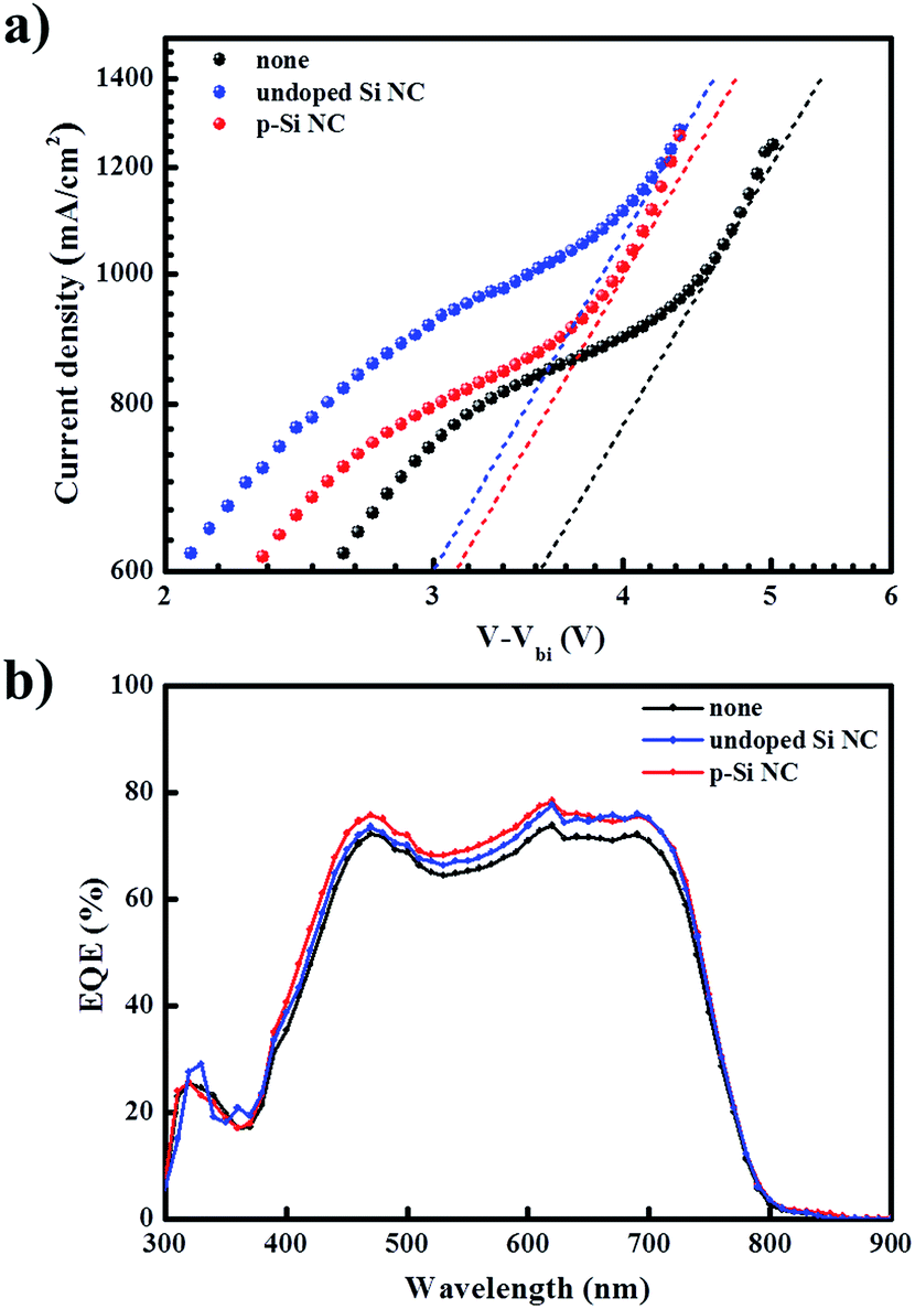 | ||
| Fig. 6 SCLC J–V characteristics obtained in the dark for hole-only devices, ITO/PEDOT:PSS/Si NCs/PTB7-Th:PC71BM/Au and (b) EQE spectra of BHJ OSCs fabricated with/without Si NCs under optimized processing conditions. | ||
Conclusions
We demonstrated the efficiency improvement in solution-processed BHJ OSCs and PHJ PrSCs by implementing Si NCs for efficient hole extraction. Additionally, we compared the HEM efficacy of undoped Si NCs and p-Si NCs in these devices. The Si NCs were prepared with an average size of ∼5 nm using a modified electrochemical etching method that provided p-Si NCs and undoped Si NCs from easily available B-doped and undoped polycrystalline silicon wafers, respectively, whilst retaining Si:H surface passivation. The p-Si NCs had a HOMO energy level that was ∼0.16 higher than that of undoped Si NCs, showing better balances with the HOMO energy levels of the PTB7-Th and MAPbI3 perovskite materials. The surface coverage of the Si–NCs on the substrate significantly affected the photovoltaic performance of the BHJ OSCs and PHJ PrSCs, resulting in PCEs enhanced by ∼6% and ∼11% in the BHJ OSCs with undoped Si NCs and p-Si NCs, respectively, and by ∼22% and ∼23% in the PHJ PrSCs with undoped Si NCs and p-Si NCs, correspondingly, compared to those without Si NC HEMs. The different efficacies of undoped Si NCs and p-Si NCs in the BHJ OSCs and PHJ PrSCs might be closely related with the balances of the HOMO values of the p-Si NCs and undoped Si NCs with those of the PTB7-Th and MAPbI3 perovskite materials. The Si NCs HEMs increased the hole mobility in the BHJ system, facilitating the hole-extraction from the polymer to the PEDOT:PSS. These results demonstrate that the Si NCs play a key role as HEMs. We believe that the findings of this study introduce a new direction for the development of high-efficiency solution-processed BHJ OSCs and PHJ PrSCs. Further studies of effective Si NC HEM approaches of various particle sizes for high efficiency devices are ongoing.Acknowledgements
This work was financially supported by Basic Science Research Program through the National Research Foundation of Korea (NRF-2015R1D1A1A01057125) and KITECH.Notes and references
- F. C. Krebs, Sol. Energy Mater. Sol. Cells, 2009, 93, 393 CrossRef CAS.
- A. C. Arias, J. D. MacKenzie, I. McCulloch, J. Rivnay and A. Salleo, Chem. Rev., 2010, 110, 3 CrossRef CAS PubMed.
- Z. He, B. Xiao, F. Liu, H. Wu, Y. Yang, S. Xiao, C. Wang, T. P. Russell and Y. Cao, Nat. Photonics, 2015, 9, 174 CrossRef CAS.
- J. Burschka, N. Pellet, S. J. Moon, R. Humphry-Baker, P. Gao, M. K. Nazeeruddin and M. Grätzel, Nature, 2013, 499, 316 CrossRef CAS PubMed.
- N. J. Jeon, J. H. Noh, Y. C. Kim, W. S. Yang, S. Ryu and S. I. Seok, Nat. Mater., 2014, 13, 897 CrossRef CAS PubMed.
- M. Liu, M. B. Johnston and H. J. Snaith, Nature, 2013, 501, 395 CrossRef CAS PubMed.
- L. Meng, J. You, T. F. Guo and Y. Yang, Acc. Chem. Res., 2016, 49, 155 CrossRef CAS PubMed.
- J. Y. Jeng, Y. F. Chiang, M. H. Lee, S. R. Peng, T. F. Guo, P. Chen and T. C. Wen, Adv. Mater., 2013, 25, 3727 CrossRef CAS PubMed.
- S. C. Price, A. C. Stuart, L. Yang, H. Zhou and W. You, J. Am. Chem. Soc., 2011, 133, 4625 CrossRef CAS PubMed.
- J. H. Heo, S. H. Im, J. H. Noh, T. N. Mandal, C. S. Lim, J. A. Chang, Y. H. Lee, H. Kim, A. Sarkar, M. K. Nazeeruddin, M. Grätzel and S. I. Seok, Nat. Photonics, 2013, 7, 486 CrossRef CAS.
- L. Etgar, P. Gao, Z. Xue, Q. Peng, A. K. Chandiran, B. Liu, M. K. Nazeeruddin and M. Grätzel, J. Am. Chem. Soc., 2012, 134, 17396 CrossRef CAS PubMed.
- M. M. Lee, J. Teuscher, T. Miyasaka, T. N. Murakami and H. J. Snaith, Science, 2012, 338, 643 CrossRef CAS PubMed.
- H. A. Atwater and A. Polman, Nat. Mater., 2010, 9, 205 CrossRef CAS PubMed.
- W. Zhang, M. Saliba, S. D. Stranks, Y. Sun, X. Shi, U. Wiesner and H. J. Snaith, Nano Lett., 2013, 13, 4505 CrossRef CAS PubMed.
- U. Würfel, D. Neher, A. Spies and S. Albrecht, Nat. Commun., 2015, 6, 6951 CrossRef PubMed.
- O. Malinkiewicz, A. Yella, Y. H. Lee, G. M. Espallargas, M. Grätzel, M. K. Nazeeruddin and H. J. Bolink, Nat. Photonics, 2014, 8, 128 CrossRef CAS.
- K. Zilberberg, S. Trost, H. Schmidt and T. Riedl, Adv. Energy Mater., 2011, 1, 377 CrossRef CAS.
- H. Zhou, Q. Chen, G. Li, S. Luo, T. B. Son, H. S. Duan, Z. Hong, J. You, Y. Liu and Y. Yang, Science, 2014, 345, 542 CrossRef CAS PubMed.
- W. Ma, C. Yang, X. Gong, K. Lee and A. J. Heeger, Adv. Funct. Mater., 2005, 15, 1617 CrossRef CAS.
- H. L. Hsu, C. P. Chen, J. Y. Chang, Y. Y. Yu and Y. K. Shen, Nanoscale, 2014, 6, 10281 RSC.
- K. Kawano, J. Sakai, M. Yahiro and C. Adachi, Sol. Energy Mater. Sol. Cells, 2009, 93, 514 CrossRef CAS.
- J. K. Lee, W. L. Ma, C. J. Brabec, J. Yuen, J. S. Moon, J. Y. Kim, K. Lee, G. C. Bazan and A. J. Heeger, J. Am. Chem. Soc., 2008, 130, 3619 CrossRef CAS PubMed.
- P. W. Liang, C. Y. Liao, C. C. Chueh, F. Zuo, S. T. Williams, X. K. Xin, J. Lin and A. K.-Y. Jen, Adv. Mater., 2014, 26, 3748 CrossRef CAS PubMed.
- A. Petersen, T. Kirchartz and T. A. Wagner, Phys. Rev. B: Condens. Matter Mater. Phys., 2012, 85, 045208 CrossRef.
- Z. Lin, C. Jiang, C. Zhu and J. Zhang, ACS Appl. Mater. Interfaces, 2013, 5, 713 CAS.
- D. Liu and T. L. Kelly, Nat. Photonics, 2014, 8, 133 CrossRef CAS.
- A. K. K. Kyaw, X. W. Sun, C. Y. Jiang, G. Q. Lo, D. W. Zhao and D. L. Kwong, Appl. Phys. Lett., 2008, 93, 221107 CrossRef.
- W. U. Huynh, J. J. Dittmer and A. P. Alivisatos, Science, 2002, 295, 2425 CrossRef CAS PubMed.
- S. Ren, L. Y. Chang, S. K. Lim, J. Zhao, M. Smith, N. Zhao, V. Bulovic, M. Bawendi and S. Gradecak, Nano Lett., 2011, 11, 3998 CrossRef CAS PubMed.
- C. Y. Liu, Z. C. Holman and U. R. Kortshagen, Adv. Funct. Mater., 2010, 20, 2157 CrossRef CAS.
- Y. Ding, R. Gresback, Q. Liu, S. Zhou, X. Pi and T. Nozaki, Nano Energy, 2014, 9, 25 CrossRef CAS.
- R. Gresback, N. J. Kramer, Y. Ding, T. Chen, U. R. Kortshagen and T. Nozaki, ACS Nano, 2014, 8, 5650 CrossRef CAS PubMed.
- H. Jeong and J. K. Lee, ACS Appl. Mater. Interfaces, 2015, 7, 28459 Search PubMed.
- Z. Yamani, H. Thompson, L. Abu Hassan and H. Nayfeh, Appl. Phys. Lett., 1997, 70, 3404 CrossRef CAS.
- D. Delley and E. F. Steigmeier, Phys. Rev. B: Condens. Matter Mater. Phys., 1993, 47, 1397 CrossRef.
- J. Jasieniak, M. Califano and S. E. Watkins, ACS Nano, 2011, 5, 5888 CrossRef CAS PubMed.
- V. D. Mihalietchi, H. X. Xie, B. de Boer, L. J. A. Koster and P. W. M. Blom, Adv. Funct. Mater., 2006, 16, 699 CrossRef.
Footnotes |
| † Electronic supplementary information (ESI) available. See DOI: 10.1039/c6ra24205g |
| ‡ The authors declare on competing financial interest. |
| This journal is © The Royal Society of Chemistry 2016 |