DOI:
10.1039/C6RA24071B
(Paper)
RSC Adv., 2016,
6, 114593-114598
Raw product of rare-earth ore works as a high-k gate insulator for low-voltage operable organic field-effect transistors†
Received
28th September 2016
, Accepted 26th November 2016
First published on 30th November 2016
Abstract
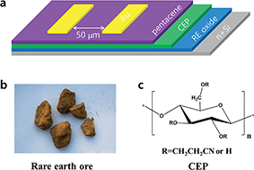
Rare earth metal oxides were found to be good candidates for high-k gate insulators in field-effect transistors. However, refinement of individual elements of rare earth metals either requires complicated processes, or discards a large fraction of the components, which drastically increases the fabrication cost and wastes natural resources. We demonstrate here the successful use of rare-earth raw product to fabricate high-quality gate insulators, which contain a number of different elements without strict refinement. The oxide dielectric thin film showed a very high dielectric constant (k) value of 35 and high dielectric strength >1 MV cm−1, which even rivals those of pure rare-earth oxides. High-k gate insulators are essential for low-voltage operated organic field-effect transistors (OFETs). Capping with a high-k cyanoethylated pullulan (CEP) polymer layer further increased the film quality and created a favorable semiconductor/dielectric interface, and benefits the stacking of overgrown semiconductor molecules. The OFETs were successfully operated at low voltage of 2–4 V, exhibiting nice mobility ∼0.5 cm2 V−1 s−1, on/off current ratio >104, and a steep subthreshold slope of 0.096 V dec−1. The utilization of rare-earth raw product as a source material would drastically reduce the production cost of gate insulators in OFETs, and reduce environmental pollution, which is meaningful in view of green chemistry.
Introduction
Organic field-effect transistors (OFETs) have attracted considerable attention for their potential applications in flexible displays, radio frequency identification (RFID) tags, electronic papers and other consumer electronics.1–5 In recent years, the field-effect mobility of organic semiconductors has been improved to more than 1 cm2 V−1 s−1.6,7 However, reducing operating voltage and creating a favorable OSC/dielectric interface are still important issues to be improved, which are determined by intrinsic properties of gate dielectrics.
To achieve low-voltage operation, high capacitance density of gate insulators is required, which can be achieved from either ultrathin or high-k gate insulators.8–12 Various rare-earth metal oxides have been reported to be excellent candidates of high-k gate dielectric materials. They are generally produced by high-vacuum process such as magnetron sputtering, atomic layer deposition (ALD) and chemical vapor deposition (CVD)13a from pure metal targets or precursors. Sol–gel processes are very promising for producing high-quality metal oxides.13b–e However, refinement processes of individual rare-earth elements either undergo complex processes, or discard many useful components. Moreover, the refinement processes and side products usually cause severe environmental problems. In fact, most rare earth metal oxides14 possibly serve as good insulators. Therefore, if the raw product of rare-earth ore without strict refinement or separation can be used, industrial cost will be significantly reduced. Moreover, high-vacuum process is not economically in both cost and time considerations, so easy solution process of simple ionic materials is desired, which can also be compatible with printing processes for low-cost mass-production.
Herein, we report the fabrication of low-voltage operable OFETs using a rare-earth ore raw product produced mixed oxide (REOx)/cyanoethylated pullulan (CEP) bilayer gate insulator. The REOx thin film was produced from an aqueous solution of rare-earth ore raw product. The thin film showed smooth dielectric surface, a high-dielectric constant (k) of 35 and excellent insulating properties to suppress electrical leakage, i.e. it shows high dielectric strength above 1 MV cm−1 and low electrical leakage around 0.1 nA. Capping with a high-k polymer layer further improved the dielectric surface for favorable semiconducting molecular growth, while did not significantly reduce the overall k value. As a result, OFETs with the bilayer gate insulator were successfully operated at very low voltages of 2–4 V, which imply that the devices can be easily functioned by a couple of dry batteries, and has great potential for use in portable and wireless electronics. The OFETs showed decent field-effect mobility, good on/off current ratio and extremely steep subthreshold slope (SS).
Experimental
Chemicals and solutions
Cylindrical green briquettes (diameter ∼ 25 mm and height ∼ 15 mm) were formed by pressing 25 g of “Bayan Obo Rare-earth complex iron ore” (RE ore), 12.71 g of coal and 7.8 pct of water (7.8 mL water mixed with 100.0 g RE ore) into a cylindrical mold for 1 min and then dried at 378 K for 4 h in the oven. Dry briquettes were placed into a graphite plate and heated at 1673 K (1400 °C) ± 5 K for 15 min.15 The samples were then taken out of the furnace and cooled down to ambient temperature rapidly. 20 g of rare-earth slag were soaked in 200 ml hydrochloric acid (1 mol L−1) for 2 hours to be dissolved into solution of the rare earth metal chloride salt. Lixivium was then achieved by filtration. CEP was dissolved in a mixed solvent of dimethylformamide (DMF) and acetonitrile (1/1 v/v) at concentration of 5% by stirring for 1 day.
Device fabrication
Highly-doped silicon wafer was cut into 2 cm × 2 cm pieces, sequentially cleaned in acetone (15 min, sonication), isopropanol alcohol (IPA) (15 min, sonication), in boiled IPA, and then blown dry using N2 gas. Rare-earth aqueous solution was spin-coated onto the cleaned substrates at 500 rpm for 5 s and 3000 rpm for 40 s. The samples were then baked at 500 °C in air. Circular-shaped gold dots were deposited as top electrodes through a shadow mask (dot size 8.02 × 10⁻⁴ cm2) to fabricate metal–insulator–metal (MIM) structures. To form an interfacial layer between the inorganic oxide and organic semiconductor, CEP was spin-coated onto the REOx thin film at 3000 rpm for 60 s, followed by baking at 60 °C in vacuum for 1 h. 40 nm organic semiconductor was deposited at a rate of 0.2–0.3 Å s−1 at a substrate temperature of 60 °C. Source/drain electrodes with a channel length of 150 μm and channel width of 1000 μm were deposited through shadow mask to form top-contact electrodes of OFET (Fig. 1).
 |
| Fig. 1 (a) Schematic demonstration of bottom-gated top-contact device architecture of an organic field-effect transistor using rare earth ore/CEP bilayer gate dielectric. (b) A photo of several pieces of rare earth ore. (c) Chemical structure of CEP polymer. | |
Characterization
Atomic force microscopy (AFM) was obtained using VEECO Dimension 3100. Scanning electron microscopy (SEM) images were obtained from an FEI Magellan 400 XHR microscope at 5 kV accelerating voltage. Electrical characteristics of OFETs were obtained from Keithley 4200 semiconductor analyzer in a N2 atmosphere.
Results and discussion
Solution of rare-earth-ore raw product
The composition of the aqueous solution of rare earth ore raw product was analyzed by inductively coupled plasma (ICP) analysis. The solution of RE ore raw product contains various kinds of ions (Table 1). The RE3+ components consist of 50% Ce, 25% La, and small amount of mixture of light rare-earth metal ions. It was reported that CeO2 and La2O3 are good candidates of high-k dielectric materials. Stacked structure of CeO2/La2O3 of gate dielectrics has been reported to reduce the amount of oxygen vacancies to significantly improve field-effect mobility in both CMOS and PMOS transistors and SS in transfer curve.16
Table 1 Components in the filtered solution (mol L−1)
Ca2+ |
RE3+ |
(SiO4)4+ |
Fe2+ |
Al3+ |
Th4+ |
0.210 |
0.060 |
0.166 |
0.020 |
0.041 |
4.11 × 10⁻⁵ |
Cross-sectional and top views of dielectric thin film
SEM image of the cross-section of a REOx thin film was captured to check the thickness of the dielectric thin film (Fig. 2). From the SEM image, a continuous film was observed with a thickness of 50 nm. AFM images were obtained to observe surface morphology of the REOx thin film (Fig. 3a). Root-mean-square (RMS) roughness was found to be 2.8 nm, which is a reasonable value for oxide thin films.17a This fabrication approach avoids high-vacuum processes and sol–gel processes, and the use of raw product of rare earth ore as a source of high-quality thin film avoids the use of well-refined materials. All these factors could ensure low-cost fabrication of the oxide dielectric thin films, and avoid severe pollution by refinement processes. Capping the thin film with high-k CEP polymer further reduce the dielectric surface RMS roughness to 0.3 nm (Fig. 3b), which is sufficiently smooth as a semiconductor/gate insulator interface. It has been reported that smooth dielectric surface can provide a substrate for the favorable stacking of over-grown semiconducting molecules.17b A smooth charge-transport channel avoid scattering and traps of charge carriers and benefits to field-effect mobility, since the field-effect conductive channel forms just within several molecular layers of the semiconductor molecules near the semiconductor/gate insulator interface.18
 |
| Fig. 2 Scanning electron microscopy image of the cross-section of the rare-earth gate dielectric thin film. | |
 |
| Fig. 3 Atomic force microscopy images of the (a) rare-earth ore thin film and (b) the CEP layer capped gate insular surface. | |
Morphology of the pentacene thin film
Smooth dielectric surface is essential for layer-by-layer stacking of pentacene molecules.19 The vertically standing pentacene molecules laterally stack to allow overlap of π bonds of the pentacene molecules to enhance charge transport along the channel direction. According to AFM image of the 40 nm-thick pentacene thin film, large grains >2 μm was observed (Fig. 4), implying good crystallinity of the thin film.
 |
| Fig. 4 Atomic force microscopy images of 40 nm pentacene on the bilayer gate insulator. (a) Top-view. (b) Three-dimensional view. | |
Leakage current and dielectric strength
Current–electric field (I–E) curve of an Au/REOx/n + Si metal–insulator–metal (MIM) structure was obtained to investigate the electrical leakage and the dielectric strength of the REOx thin film (Fig. 5). As electric field increases, the electrical current first show an increase due to acceleration of free ions, and then a saturated regime. As electric field further increases over 1 MV cm−1, electrical breakdown occurs. The curve shape is quite similar to ion avalanche as explained by Townsend discharge mechanism. Dielectric strength over 1 MV cm−1 and extremely low electrical leakage about 0.1 nA imply that the thin film possesses good insulating properties and is suitable for gate insulator application.
 |
| Fig. 5 (a) Schematic demonstration of an Au/REOx/n + Si MIM structure. (b) Electrical leakage as a function of applied electric field for a MIM structure of Au/REOx/n + Si. | |
Capacitance–frequency measurement
Capacitance as a function of frequency was recorded from MIM structure (Fig. 6). There was no significant increase in capacitance at low frequencies, which implied that, the high quality of the thin film with negligible mobile ions. According to the measured thickness and capacitance, k of REOx thin film can be calculated according to the following equation, |
 | (1) |
where C is the measured capacitance, t is the thickness of the dielectric thin film, A is the dot area of top-electrode, k is the dielectric constant of REOx, k0 is the permittivity of vacuum. A very high-k value of 35 was calculated, which even rivals those of pure rare-earth metal oxides. The total capacitance of the bilayer dielectric structure can be calculated to be 32.7 nF cm−2 from those of the REOx and CEP layers according to the following relationship. |
 | (2) |
 |
| Fig. 6 Capacitance–frequency characteristics of Au/REOx/n + Si MIM structure. | |
Organic field-effect transistor
OFETs were fabricated using a REOx/CEP bilayer gate insulator, with top-contact bottom-gate geometric architecture (Fig. 7a). Transfer and output characteristics were obtained using a probe station in a N2-filled glove box connected to a Keithley 4200 semiconductor analyzer (Fig. 7b–d). In transfer curve, drain current increased linearly with the application of negative gate voltage at low-voltage regime, and saturated at higher voltage range. The device showed a low threshold voltage (Vth) of −1.45 V and was successfully operated at voltage as low as 2 to 4 volts. The value is so small that can be driven by dry batteries for portable application. Field-effect mobility (μ) of the device was evaluated according to saturated regime of transfer curve, according to the following relationship, |
 | (3) |
where W is the channel width, L is the channel length. Field-effect mobility was calculated to be 0.5 cm2 V−1 s−1, threshold voltage is −1.45 V, on/off current ratio > 104 and SS was as low as 0.096 V dec−1. A SS of sub-0.1 V dec−1 has been reported in only very limited literatures20a and it is noteworthy to be mentioned that the value approaches the theoretical physical limit value of 0.057 V dec−1.20b
 |
| Fig. 7 (a) Schematic of the electrical characterization. (b) Transfer curve and (c) square-root of drain current as a function of gate voltage as obtained from a top-contact bottom-gated organic field-effect transistor. (d) Output curve of the field-effect transistor. | |
Evaluation of charge trap density
Charge trap density is another important parameter, since significant charge trapping and de-trapping processes could cause operational stability of OFETs. Charge trap density can be evaluated from the Vth shift and SS, according to the following equations.20c |
 | (4) |
|
 | (5) |
According to the threshold voltage shift by comparing forward and backward sweep of transfer curves, the charge trap density was calculated to be 6.60 × 10¹⁰/cm−2, while the relevant value as calculated from SS value was 3.27 × 10¹⁰/cm−2. These values are one to two magnitudes smaller than that of high-voltage operated devices,21 ensuring operational stability of the OFET. The charge trap densities as evaluated from the two distinct methods are in the same order of magnitude, which in turn verifies the accuracy of these charge-trap density values, as well as the accuracy of threshold voltages and SS.
Conclusion
High-quality gate insulator was obtained from aqueous solution of rare-earth ore raw product. These thin films showed good insulating properties, such as high k value of 35 and high dielectric strength larger than 1 MV cm−1. OFETs with a polymer coated RE oxide thin film as a gate insulator can be successfully operated at low-voltage of 2–4 V, and showed field-effect mobility of ∼0.5 cm2 V−1 s−1, on/off current ratio > 104, and steep SS of ∼0.096 V dec−1. This paper represents important progress in fabrication of low-voltage organic field-effect transistors for future low-power electronics, and the use of rare-earth raw product instead of use refined rare-earth metal based precursors as a source material for high quality gate insulator would significantly reduce the fabrication cost and avoid the severe pollution in refining processes.
Acknowledgements
The authors gratefully acknowledge the support of National Natural Science Foundation of China (No. 51304015) and the State Key laboratory of Advanced Metallurgy, University of Science and Technology Beijing (No. 41614007).
References
- Y. Guo, G. Yu and Y. Liu, Adv. Mater., 2010, 22, 4427 CrossRef CAS PubMed.
- K. K. Banger, Y. Yamashita, K. Mori, R. L. Peterson, T. Leedham, J. Rickard and H. Sirringhaus, Nat. Mater., 2011, 10, 45 CrossRef CAS PubMed.
- J. Rivnay, L. H. Jimison, M. F. Toney, R. Noriega, T. J. Marks, A. Facchetti and A. Salleo, Nat. Mater., 2009, 8, 952 CrossRef CAS PubMed.
- D. Y. Khang, H. Q. Jiang, Y. Huang and J. A. Rogers, Science, 2006, 311, 208 CrossRef CAS PubMed.
- L. Qiu, W. H. Lee, X. Wang, J. S. Kim, J. A. Lim, D. Kwak, S. Lee and K. Cho, Adv. Mater., 2009, 21, 1349 CrossRef CAS.
- Y. Yamashita, Sci. Technol. Adv. Mater., 2009, 10, 024313 CrossRef PubMed.
- A. Facchetti, Mater. Today, 2007, 10, 28 CrossRef CAS.
- M. Halik, H. Klauk, U. Zschieschang, G. Schmid, C. Dehm, M. Schütz, S. Maisch, F. Effenberger, M. Brunnbauer and F. Stellacci, Nature, 2004, 431, 963 CrossRef CAS PubMed.
- A. Facchetti, M. H. Yoon and T. J. Marks, Adv. Mater., 2005, 17, 1705 CrossRef CAS.
- C. D. Dimitrakopoulos, S. Purushothaman, J. Kymissis, A. Callegari and J. M. Shaw, Science, 1999, 283, 822 CrossRef CAS PubMed.
-
(a) R. P. Ortiz, A. Facchetti and T. J. Marks, Chem. Rev., 2010, 110, 205 CrossRef CAS PubMed;
(b) W. Xu, C. Guo and S.-W. Rhee, J. Mater. Chem. C, 2013, 1, 3955 RSC.
-
(a) B. N. Pal, B. M. Dhar, K. C. See and H. E. Katz, Nat. Mater., 2009, 8, 898 CrossRef CAS PubMed;
(b) W. Huang, K. Besar, Y. Zhang, S. Yang, G. Wiedman, Y. Liu, W. Guo, J. Song, K. Hemker, K. Hristova, I. J. Kymissis and H. E. Katz, Adv. Funct. Mater., 2015, 25, 3745 CrossRef CAS;
(c) B. Zhang, Y. Liu, S. Agarwal, M.-L. Yeh and H. E. Katz, ACS Appl. Mater. Interfaces, 2011, 3, 4254 CrossRef CAS PubMed.
-
(a) G. Bonnet, M. Lachkar, J. P. Larpin and J. C. Colson, Solid State Ionics, 1994, 72, 344 CrossRef CAS;
(b) W. Hu, B. Frost and R. L. Peterson, J. Phys. D: Appl. Phys., 2016, 49, 115109 CrossRef;
(c) K. Song, W. Yang, Y. Jung, S. Jeong and J. Moon, J. Mater. Chem., 2012, 22, 21265 RSC;
(d) A. Garcia-Murillo, C. LeLuyer-Urlacher, C. Dujardin, C. Pédrini and J. Mugnier, J. Sol-Gel Sci. Technol., 2003, 26, 957 CrossRef CAS;
(e) Q. Kuang, Z.-W. Lin, W. Lian, Z.-Y. Jiang, Z.-X. Xie, R.-B. Huang and L.-S. Zheng, J. Solid State Chem., 2007, 180, 1236 CrossRef CAS.
- B.-H. Lei, Q. Kong, Z. Yang, Y. Yang, Y. Wang and S. Pan, J. Mater. Chem. C, 2016, 4, 6295 RSC.
- Y. Ding, Q. Xue, G. Wang and J. Wang, Metall. Mater. Trans. B, 2013, 44, 28 CrossRef CAS.
- B. L. Yang, H. Wong, K. Kakushima and H. Iwai, Microelectron. Reliab., 2012, 52, 1613 CrossRef CAS.
-
(a) J.-M. Kim, P. Thiyagarajan and S.-W. Rhee, Thin Solid Films, 2010, 518, 5860 CrossRef CAS;
(b) S. Steudel, S. D. Vusser, S. D. Jonge, D. Janssen, S. Verlaak, J. Genoe and P. Heremans, Appl. Phys. Lett., 2004, 85, 4400 CrossRef CAS.
- Y. Zhang, J. Qiao, S. Gao, F. Hu, D. He, B. Wu, Z. Yang, B. Xu, Y. Li, Y. Shi, W. Ji, P. Wang, X. Wang, M. Xiao and H. Xu, Phys. Rev. Lett., 2016, 116, 016602 CrossRef PubMed.
- W. Xu, F. Wang and S.-W. Rhee, J. Mater. Chem., 2012, 22, 1482 RSC.
-
(a) U. Zschieschang, M. J. Kang, K. Takimiy, T. Sekitani, T. Someya, T. W. Canzler, A. Werner, J. Blochwitz-Nimothd and H. Klauk, J. Mater. Chem., 2012, 22, 4273 RSC;
(b) S. M. Sze and K. K. Ng, Physics of semiconductor devices, Wiley, New York, 3rd edn, 2006 Search PubMed;
(c) W. Xu and S.-W. Rhee, J. Mater. Chem., 2009, 19, 5250 RSC.
- W. Xu and S.-W. Rhee, Org. Electron., 2010, 11, 836 CrossRef CAS.
Footnote |
† Electronic supplementary information (ESI) available. See DOI: 10.1039/c6ra24071b |
|
This journal is © The Royal Society of Chemistry 2016 |
Click here to see how this site uses Cookies. View our privacy policy here.