
A galvanic replacement reaction to synthesise metal/ZnO heterostructured films on zinc substrates for enhanced photocatalytic performance†
Kai Wangab,
Zhangxian Chena,
Mengqiu Huanga,
Zeheng Yanga,
Chunyan Zenga,
Lei Wanga,
Maoqin Qiua,
Yingmeng Zhanga and
Weixin Zhang*a
aSchool of Chemistry and Chemical Engineering, Hefei University of Technology, Hefei, 230009, Anhui, China. E-mail: wxzhang@hfut.edu.cn
bSchool of Chemistry and Chemical Engineering, Beifang University of Nationality, Ningxia, Yinchuan, 750021, China
First published on 24th October 2016
Abstract
The construction of non-precious transition metal/ZnO heterostructured films is being considered as an effective way to promote photocatalytic efficiency for their practical applications. Herein, a general and facile approach is reported for the first time to synthesize a series of M/ZnO (M = Cu, Cd, Co) heterostructured films on Zn substrate based on a simple one-step galvanic replacement reaction between Zn substrate and metal salt solution under hydrothermal condition without the use of any other reactants or additives. Zn substrate functions as not only the reducing agent, but also the source of ZnO to simplify the recipes and facilitate the synthetic procedures. Among M/ZnO heterostructured films, due to their matching degree of phase and cell parameters, two kinds can be prepared, including Cu/ZnO and Co/ZnO heterostructures with metal nanoparticles (e.g. Cu and Co) anchored on ZnO nanorods and Cd/ZnO heterostructures assembled by Cd nanorod core and ZnO nanorod branches. A pine tree-like Cu/ZnO heterostructured film is chosen as a representative to demonstrate the facility and effectiveness of the strategy, which exhibits higher photocatalytic efficiency towards visible light irradiation than bare ZnO nanospindles. The enhanced photocatalytic activities may be mainly attributed to the surface plasmon absorption of Cu nanoparticles in the visible region, which increases the optical absorption of the Cu/ZnO heterostructures and promotes the transfer of photo-induced electrons from Cu nanoparticles into ZnO nanorods. This general method can be further explored to guide the design of metal/metal oxide heterostructured films on other substrates, such as Cu, Ni and Ti foils.
1. Introduction
Heterostructures, integrated by multiple functional components, have encouraged tremendous interest because of their unique electrical and optical properties and wide applications in photocatalysis, optics and solar cells.1–7 Zinc oxide (ZnO), with a band gap larger than 3 eV, has been considered as an important photocatalyst for the degradation of organic pollutants under UV-light irradiation.8,9 However, the photocatalytic performance of ZnO nanostructures is relatively low due to the narrow light response range and poor separation of photogenerated charge carriers. One reported strategy to overcome these drawbacks is to combine ZnO with noble metal to form heterostructures.10,11 Under visible light irradiation, noble metal nanoparticles, like Au and Ag, have strong optical absorption and photo-induced electrons can be generated near the surfaces of the noble metal nanoparticles due to surface plasmon resonance (SPR).12–14 The photo-induced electrons can be rapidly transferred from noble metal to the conduction band (CB) of ZnO, and thus provide charge separation, which are beneficial for photocatalysis performance of heterostructured Au/ZnO and Ag/ZnO.However, the large-scale synthesis and commercial application of photocatalysts with noble metal/ZnO heterostructures would be hampered by the limited resources and high cost of noble metals. An effective way to solve these problems is to incorporate low-cost and non-precious transition metals into the hybrid nanostructures, such as Cu/ZnO heterostructure. Copper in the same elemental group with silver and gold has been observed with strong SPR in the visible region.15 Flomin et al.16 have synthesized metal Cu/ZnO nanopyramid powder via high-temperature decomposition of copper acetylacetonate and zinc acetate in oleic acid/oleylamine and they did not investigate the photocatalytic property of Cu/ZnO heterostructure. Additionally, the powder form photocatalyst couldn't avoid problems of easy agglomeration and difficult separation for their practical applications.
Recently, our group has reported a strategy of self-sustained cycle of hydrolysis and etching at solution/solid interfaces to prepare metal oxide micro/nanostructured arrays films on metal substrates.17 Inspired by the work, in this article, we report a general and facile synthetic strategy to fabricate a series of M/ZnO (M = Cu, Cd, Co) heterostructured films on zinc substrate under hydrothermal condition. The synthetic system simply involves zinc substrate and metal salt solution based on a spontaneous galvanic replacement reaction without the use of any other reactants or additives. On condition that the standard electrode potentials of metal cation/metal (Mn+/M) are higher than that of Zn2+/Zn (−0.76 V), (i.e. >−0.76 V), the galvanic replacement reaction readily occurs at the interfaces between metal salt solutions and zinc substrates. It is interesting to observe that zinc substrate functions as not only a reductant to reduce less active metal ion into metal, but also a source of zinc oxide. Based on their matching degree on cell parameters, two kinds of M/ZnO hierarchical heterostructured films can be prepared, including Cu/ZnO and Co/ZnO heterostructures with metal nanoparticles (e.g. Cu and Co) anchored on ZnO nanorods and Cd/ZnO heterostructures assembled by Cd nanorod core and ZnO nanorod branches. Herein, a pine tree-like Cu/ZnO heterostructured film is chosen as a representative to demonstrate the facility and effectiveness of the strategy, which exhibits higher photocatalytic efficiency towards visible light irradiation.
2. Experimental section
2.1 Synthesis of M/ZnO heterostructured films on Zn substrate
2.2 Characterization
The crystal structures of the samples were examined by a Rigaku D/max-γ B X-ray diffractometer with a Cu Kα radiation source (λ = 0.154178 nm), operated at 40 kV and 80 mA. The morphology was characterized by the field-emission scanning electron microscopy (FESEM, Sirion-200). Elemental mappings and field-emission transmission electron microscopy (FETEM) images were acquired on a JEM-2100F FETEM. X-ray photoelectron spectroscopy (XPS) was performed on a Thermo ESCALAB 250 spectrometer using an Al Kα X-ray source (hν = 1486.6 eV) with a pass energy of 20 eV. The optical absorption spectra were recorded using a UV-visible spectrophotometer (Shimadzu UV-2550) in the wavelength from 200 to 800 nm. The concentration of Zn2+ ions in solution was detected by the atomic absorption spectroscopy (Perkin Eimei, AA80).2.3 Photocatalytic activity measurement
The photocatalytic activities of the heterostructured catalysts were assessed by the degradation of aqueous methyl orange (MO) dye solution under illumination of visible light. A quartz cuvette (1 cm) and xenon lamp (500 W) were used as the photocatalytic reactor and source of visible light, respectively. The distance between the reactor and light source was kept at approximately 3 cm. Initially, 3 mL of MO dye solution (10 mg L−1) was transferred into the photocatalytic reactor. Subsequently, a piece of Cu/ZnO heterostructured film was vertically immersed into the solution in face of the light source. The reaction system was kept at dark for 2 h to reach the adsorption/desorption equilibrium. After each time interval of 30 min, the film was removed from the cuvette. The concentrations of MO dye solution were analyzed by a UV-vis spectrophotometer based on the linear calibration curve.3. Results and discussion
To avoid the strong signal from zinc substrate, several pieces of Cu/ZnO heterostructured film on zinc substrate were scraped and collected for XRD measurement. The XRD pattern (Fig. 1) of the sample synthesized at 80 °C for 24 h with the Cu2+ ions of 0.6 mL can be indexed to the cubic Cu (JCPDS no. 04-0836) and hexagonal wurtzite ZnO (JCPDS no. 36-1451).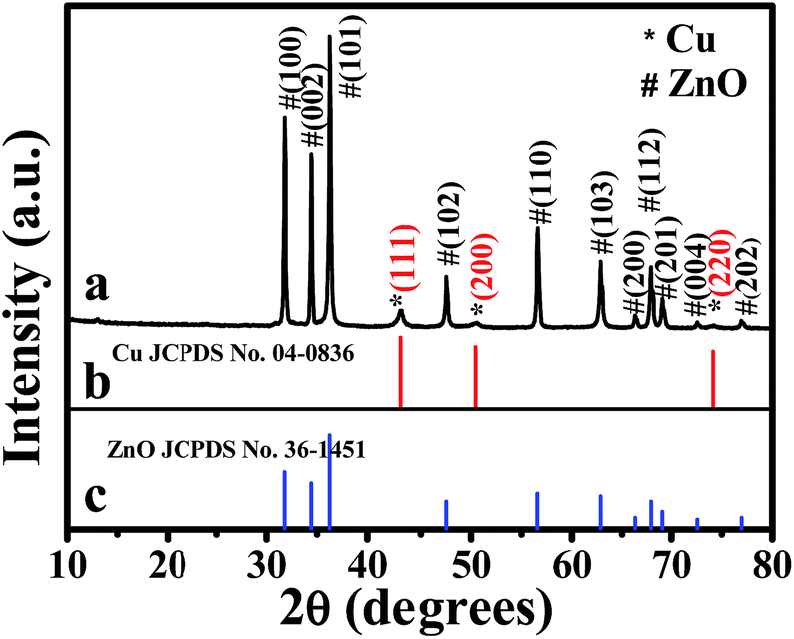 | ||
| Fig. 1 (a) XRD pattern of the typical scraped Cu/ZnO heterostructured film on zinc substrate and the standard patterns of (b) Cu and (c) wurtzite ZnO. | ||
Fig. S1† presents morphological variations of Cu/ZnO heterostructured film on zinc substrate at the reaction times of 1 h, 3 h, 6 h and 12 h. We find the morphologies gradually transfers from the aggregates to the rod-like and eventually into the tree-like structures when extending the reaction time from 1 h to 3 h, 6 h and finally 12 h. When the reaction time is further increased to 24 h, the well-defined pine tree-like heterostructure with the lengths up to tens of microns can be obtained. The FESEM images (Fig. 2a and b) show the pine tree-like morphology of the Cu/ZnO heterostructure arrays. Cu nanoparticles with tens of nanometers in size are well dispersed on ZnO nanorods. Fig. 2c presents the TEM image of a typical broken pine tree-like branch. The corresponding HRTEM image (Fig. 2d) clearly exhibits the respective domains of Cu and ZnO and the interface in Cu/ZnO heterostructure, as indicated by the lattice fringes of Cu (111) and ZnO (002), respectively. The STEM image (Fig. 2e) and the related elemental mappings (Fig. 2f–h) suggest that Cu, Zn and O are well dispersed along the rod in the Cu/ZnO heterostructure. The corresponding energy-dispersive X-ray spectroscopy (EDS) spectrum (Fig. 2i) indicates that the atomic ratios of Cu, Zn and O are about 9.44![[thin space (1/6-em)]](https://www.rsc.org/images/entities/char_2009.gif) :45.79:44.77, respectively.
:45.79:44.77, respectively.
 | ||
| Fig. 2 (a and b) Low and high resolution FESEM images of pine tree-like Cu/ZnO heterostructured film on zinc substrate prepared by a hydrothermal method at 80 °C for 24 h with 0.6 mM Cu2+. (c) TEM image of a broken pine tree-like branch. (d) HRTEM image corresponding to the circled region in (c). (e) STEM image, (f–h) the related elemental mappings and (i) EDS spectrum of a single pine tree-like Cu/ZnO. | ||
The XPS survey spectrum (Fig. 3a) of the pine tree-like Cu/ZnO heterostructured film indicates that in reference to the aliphatic C 1s peak (284.96 eV), elements of Cu, Zn and O can be detected. The binding energies of Cu 2p3/2 and Cu 2p1/2 are located at 932.48 eV and 952.18 eV, respectively (Fig. 3b), with a spin–orbital splitting of 19.7 eV and the intensity ratio of 0.48. In addition, no obvious satellite peak can be observed, suggesting that copper exists in zero valent in the Cu/ZnO heterostructured film.18,19 The binding energies of Zn 2p3/2 and Zn 2p1/2 are 1021.37 eV and 1044.88 eV, respectively (Fig. 3c), which can be ascribed to Zn2+ ions in ZnO.20 The binding energy of O 1s at 530.73 eV is associated with the lattice oxygen of ZnO (Fig. 3d).21
 | ||
| Fig. 3 XPS spectra of the pine tree-like Cu/ZnO heterostructured film on zinc substrate: (a) survey spectrum, and core-level spectra of (b) Cu 2p, (c) Zn 2p and (d) O 1s. | ||
Scheme 1 illustrates the synthesis of pine tree-like Cu/ZnO heterostructured film based on the galvanic replacement reaction on zinc substrate under hydrothermal condition. Cu nanoparticles are obtained from the galvanic replacement reaction between Cu2+ coming from CuCl2 solution and Zn foil (eqn (1),  vs.
vs.  ). Meanwhile, the oxygen molecules
  dissolved in the solution can oxidize zinc foil to ZnO and itself is reduced into OH− ions (eqn (2)) under hydrothermal condition, which has been confirmed by the increasing pH value with the reaction progress (Fig. S2, ESI†).22 The overall reaction can be expressed by eqn (3). The formation of Zn2+ ions has been confirmed by the atomic absorption spectroscopy ([Zn2+] = 36.71 mg L−1 in the final solution). Finally, a typical pine tree-like Cu/ZnO heterostructure is formed through the self-assembly of Cu nanoparticles and ZnO nanorods, as illustrated in Scheme 1. The involved reactions are shown as follows.
| Zn(s) + Cu2+(aq) → Zn2+(aq) + Cu(s) | (1) |
| 2Zn(s) + O2 + H2O → ZnO(s) + Zn2+(aq) + 2OH− | (2) |
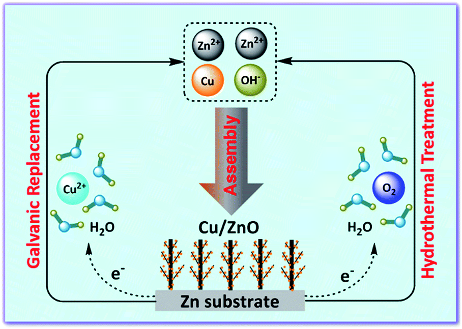 | ||
| Scheme 1 A schematic illustration of synthesizing pine tree-like Cu/ZnO heterostructured film on zinc substrate based on the galvanic replacement reaction. | ||
Total reaction:
 | (3) |
Promisingly, in our study, we have successfully extended our method to synthesize Co/ZnO and Cd/ZnO heterostructured films on zinc substrate based on galvanic replacement reaction by replacing CuCl2 solution with the CoCl2  and CdCl2
  solutions, respectively.
Different from the Cu/ZnO heterostructure morphology, Cd/ZnO exhibits an interesting brush-like heterostructured film on zinc substrate (Fig. 4). Hexagonal Cd (JCPDS no. 05-0674) and wurtzite hexagonal ZnO (JCPDS no. 36-1451) can be indexed from the XRD pattern (Fig. 4a) and its low and high magnification FESEM images show the brush-like morphology of Cd/ZnO heterostructure with ∼50 μm in length (Fig. 4b and c). The EDS spectrum (Fig. 4d) indicates the atomic ratios of Cd, Zn and O is 18.5:37.1:44.4, respectively. Surprisingly, the elemental mappings (Fig. 4e–h) of a broken brush-like Cd/ZnO heterostructure (Fig. 4e) indicate that it is assembled by the Cd nanorod core with 1–2 μm in diameter and ZnO nanorod branches with 2–5 μm in length. Regretfully, due to metal Cd with a very low melting point (320.9 °C),23 HRTEM analysis cannot be conducted for further study. But we speculate that the ZnO branched nanorods based on Cd core microrod through the heteroepitaxial growth process because ZnO and Cd both belong to hexagonal phase with similar cell parameters.24,25
 | ||
| Fig. 4 (a) XRD pattern of the typical scraped Cd/ZnO heterostructured film on zinc substrate. (b and c) Low and high resolution FESEM images and (d) the corresponding EDS spectrum of brush-like Cd/ZnO heterostructured film on zinc substrate. (e) FESEM image of a broken brush-like Cd/ZnO heterostructure and (f–h) the related elemental mappings of Cu, Zn and O on Si substrate. | ||
The XRD pattern (Fig. 5a) of Co/ZnO heterostructured film can be indexed to hexagonal Co (JCPDS no. 05-0727) and ZnO (JCPDS no. 36-1451). The FESEM images (Fig. 5b and c) indicate the flower-like morphologies Co/ZnO heterostructured films. The elemental mappings and the corresponding EDS spectrum suggest the co-existence of Co, Zn and O with atomic ratios of 3.8%, 52.9% and 43.3%, respectively (Fig. 5d–h). It is clearly shown that Co nanoparticles are well dispersed along the ZnO nanorod. Although Co has hexagonal phase, its lattice parameters are much smaller than that of hexagonal ZnO, the mismatch degree of which also makes Co display nanoparticles incorporated on ZnO nanorods (Table S1, ESI†).
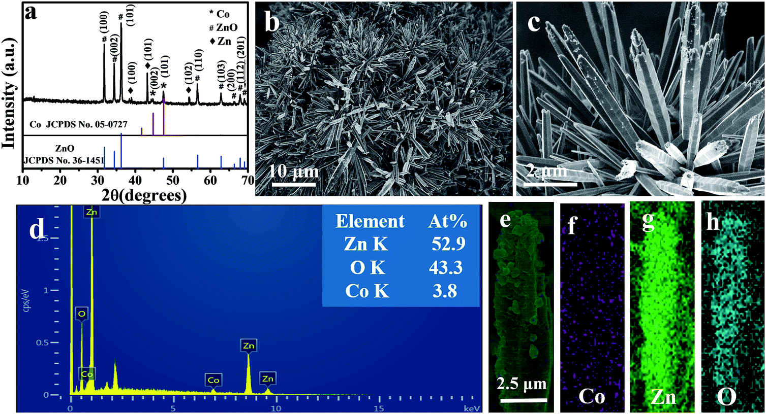 | ||
| Fig. 5 (a) XRD pattern of Co/ZnO heterostructured film on zinc substrate. (b and c) Low and high resolution FESEM images and (d) the corresponding EDS spectrum of flower-like Co/ZnO heterostructured film on zinc substrate. (e) FESEM image of a piece of flower-like Co/ZnO heterostructure and (f–h) the related elemental mappings of Cu, Zn and O on Si substrate. | ||
On the other hand, if the standard electrode potential value of Mn+/M  is lower than that of Zn2+/Zn, the galvanic replacement reaction cannot proceed spontaneously. For instance, Mg/ZnO film cannot be obtained by the reaction between Mg(Ac)2 solution and Zn substrate under the same reaction condition since the
 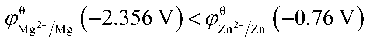 . Thus, only ZnO nanospindles are formed on the zinc substrate (Fig. S3, ESI†). Table S2 of ESI† lists the standard electrode potentials of some Mn+/M.23
To sum up, this novel synthetic strategy is facile and effective to fabricate a series of M/ZnO (M = Cu, Co, Cd) heterostructured films on zinc substrate. It can be scaled up to prepare the heterostructured film on large-area substrate for practical applications (e.g. 40 cm2 for Cu/ZnO heterostructured film, Fig. S4, ESI†). In addition, it has several advantages: (i) the M/ZnO heterostructured films can be synthesized via a simple one-step process; (ii) the reactions only involve zinc foil and metal salt solutions without using any other reactants or additives; (iii) the synthetic strategy could be hopefully extended to prepare metal/metal oxide heterostructures supported on other substrates.
To evaluate the photocatalytic activities of the as-prepared Cu/ZnO heterostructured films under visible light irradiation, methyl orange (MO) has been used as a model pollutant. The concentrations of MO were determined using UV-visible absorption spectroscopy (Fig. S5, ESI†). Fig. 6a compares the photocatalytic performances of the different catalysts. The related time-dependent UV-vis absorption spectra of MO solution are shown in Fig. S6 of ESI.† Obviously, the degradation ratio of MO is only about 9% after 4.5 h without using any photocatalyst, which increases to 59% with bare ZnO nanospindle film as the catalyst. The Cu/ZnO heterostructured films prepared with the volumes of CuCl2 (20 mM) solution of 0.2, 0.6 and 2.0 mL show the increasing degradation ratios of 67%, 91% and 81%, respectively. The Co/ZnO and Cd/ZnO heterostructured films also display the degradation ratios of 82.5% and 67%, respectively under the same catalytic conditions (Fig. S7, ESI†) implying their potential applications in the photocatalytic degradation of organic pollutants.
 | ||
| Fig. 6 (a) Photocatalytic degradations of MO solution under visible light irradiation with blank and different photocatalysts. (b) Recyclability of the pine tree-like Cu/ZnO heterostructured film (S2) in the photocatalytic degradation of MO solution. (c) UV-vis diffuse absorption spectra and (d) the corresponding Tauc plots of bare ZnO nanospindle film and Cu/ZnO heterostructured films synthesized with different concentrations of Cu2+ (S1, S2 and S3 refer to Cu/ZnO heterostructured films prepared with 0.2, 0.6 and 2.0 mL of CuCl2 solution (20 mM) on zinc substrate, respectively. Initial concentration of MO: C0 = 10 mg L−1). | ||
Fig. 6b presents the recyclability of the pine tree-like Cu/ZnO heterostructure in the photocatalytic degradation of MO. As observed, the MO degradation ratio gradually decreases from 91% to 81% after five cycles. Some active sites on the surface of the pine tree-like Cu/ZnO heterostructure may be partly blocked by the decomposed organic species.26,27 Overall, the Cu/ZnO heterostructured film exhibit a good stability as the photocatalyst during the photocatalytic degradation of methyl orange solution. After the fifth catalysis cycles, the Cu/ZnO heterostructured catalyst did not show obvious changes of XRD pattern (Fig. S8†), XPS spectra (Fig. S9†) and morphologies (Fig. S10†), demonstrating the stability of the catalyst.
It is known that the light absorption abilities of semiconductors are important factors to evaluate their photocatalytic activities. The room temperature UV-visible diffuse reflectance spectroscopy analysis is conducted for the Cu/ZnO heterostructured films and bare ZnO nanospindle film (Fig. 6c). Compared with bare ZnO nanospindle film (Fig. S11, ESI,†), the Cu/ZnO heterostructured films exhibit obvious red shift in optical absorbance, which may be attributed to the SPR effect of spatially confined electrons in metallic copper nanoparticles.28,29 The corresponding Tauc plots of Fig. 4c are shown in Fig. 6d, where α and hν refer to the absorption coefficient and photon energy, respectively.30 The band gap energy of bare ZnO nanospindle film is calculated to be 3.16 eV. The band gap energies of Cu/ZnO heterostructured films prepared with 0.2 mM, 0.6 mM and 2.0 mM of Cu2+ are calculated to be 3.08 eV, 2.95 eV and 2.68 eV, respectively, which indicate that the incorporation of Cu nanoparticles can increase the light absorption abilities and gradually shift the absorption wavelength of ZnO from UV to visible region.
The increase in the photocatalytic performances could be resulted from the following reasons. The first one is the surface plasmon absorption of Cu nanoparticles in the visible region, and the second is that Cu/ZnO heterostructures promote the transfer of photo-induced electrons from Cu nanoparticles to ZnO nanorods owing to higher SPR band position of Cu than the conduction band of ZnO and effectively improve the separation of the photogenerated electron–hole pairs, thus increasing the catalytic efficiency.28,31 Furthermore, as revealed in Fig. 4c, the heterostructures shift the optical absorption edge towards the visible range and increase the cross section of light absorption.15,32 Therefore, it shows the highest photocatalytic activity of 91%. However, the Cu/ZnO heterostructured film fabricated with 2.0 mL of CuCl2 solution displays a lower heterostructures shift the optical absorption edge towards the visible range and increase the cross section of light efficiency of 81%. The decreased photocatalytic activity can be attributed to the increasing recombination of the photoelectrons and holes as a result of the high loading of the Cu nanoparticles.33,34
4. Conclusion
In conclusion, a general and facile approach is reported for the first time to synthesize a series of M/ZnO (M = Cu, Cd, Co) heterostructured films on Zn substrate based on a simple one-step galvanic replacement reaction between Zn substrate and metal salt solution under hydrothermal condition without the use of any other reactants or additives. Considering the matching degree of phase and cell parameters, two kinds of M/ZnO heterostructured films can be prepared, including Cu/ZnO and Co/ZnO heterostructures with metal nanoparticles (e.g. Cu and Co) anchored on ZnO nanorods and Cd/ZnO heterostructure assembled by Cd nanorod core and ZnO nanorod branches. This general method can be further explored to synthesize metal/metal oxide heterostructured films on other substrates, such as Cu, Ni and Ti foils. Herein, a pine tree-like Cu/ZnO heterostructured film is chosen as a representative to demonstrate the facility and effectiveness of the strategy, which exhibits higher photocatalytic efficiency towards visible light irradiation. The enhanced photocatalytic activities may be mainly attributed to the surface plasmon absorption of Cu nanoparticles in the visible region. Cu/ZnO heterostructures promote the transfer of photo-induced electrons from Cu nanoparticles to ZnO nanorods owing to SPR and increase the cross section of optical absorption in visible range.Acknowledgements
The authors are grateful to the financial supports from the National Natural Science Foundation of China (NSFC Grants 21271058 and 91534102). This work is also supported by Science and Technology Project of Anhui Province (1501021013) and Intelligent Manufacturing Institute of Hefei University of Technology (IMICZ2015104).References
- R. B. Jiang, B. X. Li, C. H. Fang and J. F. Wang, Adv. Mater., 2014, 26, 5274–5309 CrossRef CAS PubMed.
- S. T. Kochuveedu, Y. H. Jang and D. H. Kim, Chem. Soc. Rev., 2013, 42, 8467–8493 RSC.
- H. L. Wang, L. S. Zhang, Z. G. Chen, J. Q. Hu, S. J. Li, Z. H. Wang, J. S. Liu and X. C. Wang, Chem. Soc. Rev., 2014, 43, 5234–5244 RSC.
- U. Banin, Y. Ben-Shahar and K. Vinokurov, Chem. Mater., 2014, 26, 97–110 CrossRef CAS.
- Y. J. Wang, Q. S. Wang, X. Y. Zhan, F. M. Wang, M. Safdar and J. He, Nanoscale, 2013, 5, 8326–8339 RSC.
- D. P. Wu, K. Cao, F. J. Wang, H. J. Wang, Z. Y. Gao, F. Xu, Y. M. Guo and K. Jiang, Chem. Eng. J., 2015, 280, 441–447 CrossRef CAS.
- D. P. Wu, F. J. Wang, H. J. Wang, K. Cao, Z. Y. Gao, F. Xu and K. Jiang, Dalton Trans., 2016, 45, 16275–16282 RSC.
- C. Q. Chen, Y. H. Zheng, Y. Y. Zhan, X. Y. Lin, Q. Zheng and K. Wei, Dalton Trans., 2011, 40, 9566–9570 RSC.
- D. P. Wu, Z. Y. Gao, F. Xu, J. L. Chang, W. G. Tao, J. J. He, S. Y. Gao and K. Jiang, CrystEngcomm, 2013, 15, 1210–1217 RSC.
- Y. Q. Sun, Y. G. Sun, T. Zhang, G. Z. Chen, F. S. Zhang, D. L. Liu, W. P. Cai, Y. Li, X. F. Yang and C. C. Li, Nanoscale, 2016, 8, 10774–10782 RSC.
- S. W. Wang, Y. Yu, Y. H. Zuo, C. Z. Li, J. H. Yang and C. H. Lu, Nanoscale, 2012, 4, 5895–5901 RSC.
- Y. Z. Chen, D. Q. Zeng, K. Zhang, A. L. Lu, L. S. Wang and D. L. Peng, Nanoscale, 2014, 6, 874–881 RSC.
- A. Ghosh, P. Guha, A. K. Samantara, B. K. Jena, R. Bar, S. Ray and P. V. Satyam, ACS Appl. Mater. Interfaces, 2015, 7, 9486–9496 CAS.
- C. Mondal, J. Pal, M. Ganguly, A. K. Sinha, J. Jana and T. Pal, New J. Chem., 2014, 38, 2999–3005 RSC.
- W. B. Hou and S. B. Cronin, Adv. Funct. Mater., 2013, 23, 1612–1619 CrossRef CAS.
- K. Flomin, I. Jen-La Plante, B. Moshofsky, M. Diab and T. Mokari, Nanoscale, 2014, 6, 1335–1339 RSC.
- Y. M. Zhang, W. X. Zhang, Z. H. Yang, H. Y. Gu, Q. Zhu, S. H. Yang and M. Li, Angew. Chem., Int. Ed., 2015, 127, 4004–4008 CrossRef.
- G. Deroubaix and P. Marcus, Surf. Interface Anal., 1992, 18, 39–46 CrossRef CAS.
- V. Bansal, H. Jani, J. D. Plessis, P. J. Coloe and S. K. Bhargava, Adv. Mater., 2008, 20, 717–723 CrossRef CAS.
- Y. L. Xie, S. K. Yang, Z. M. Mao, P. Li, C. L. Zhao, Z. Cohick, P. H. Huang and T. J. Huang, ACS Nano, 2014, 8, 12175–12184 CrossRef CAS PubMed.
- K. Milenova, I. Avramova, A. Eliyas, V. Blaskov, I. Stambolova and N. Kassabova, Environ. Sci. Pollut. Res., 2014, 21, 12249–12256 CrossRef CAS PubMed.
- W. X. Zhang and S. H. Yang, Acc. Chem. Res., 2009, 42, 1617–1627 CrossRef CAS PubMed.
- J. A. Dean, Lange's handbook of chemistry, McGraw-Hill, New York, 13th edn, 1985 Search PubMed.
- H. X. Chen, M. Wen, Z. D. Huang, Q. S. Wu, J. L. Liu and T. Tu, J. Mater. Chem. A, 2015, 3, 600–607 CAS.
- Z. Q. Wang, J. Wang, T. K. Sham and S. G. Yang, J. Phys. Chem. C, 2012, 116, 10375–10381 CAS.
- W. X. Zhang, G. D. Chen, Z. H. Yang and C. Y. Zeng, AIChE J., 2013, 59, 2134–2144 CrossRef CAS.
- G. D. Chen, H. Cheng, W. X. Zhang, Z. H. Yang, M. Q. Qiu, X. Zhu and M. Chen, AIChE J., 2015, 61, 1478–1482 CrossRef CAS.
- J. Pal, A. K. Sasmal, M. Ganguly and T. Pal, J. Phys. Chem. C, 2015, 119, 3780–3790 CAS.
- J. J. Zhang, H. Y. Gu, X. N. Yang, M. Chen, Z. H. Yang and W. X. Zhang, RSC Adv., 2015, 5, 8537–8543 RSC.
- S. J. Peng, L. L. Li, H. T. Tan, Y. Z. Wu, R. Cai, H. Yu, X. Huang, P. N. Zhu, S. Ramakrishna, M. Srinivasanab and Q. Y. Yan, J. Mater. Chem. A, 2013, 1, 7630–7638 CAS.
- X. M. Hou, Mater. Lett., 2015, 139, 201–204 CrossRef CAS.
- K. G. Kanade, B. B. Kale, J. O. Baeg, S. M. Lee, C. W. Lee, S. J. Moon and H. Chang, Mater. Chem. Phys., 2007, 102, 98–104 CrossRef CAS.
- S. Sun, H. Z. Liu, L. Wu, C. E. Png and P. Bai, ACS Catal., 2014, 4, 4269–4276 CrossRef CAS.
- D. W. Ding, K. Liu, S. N. He, C. B. Gao and Y. D. Yin, Nano Lett., 2014, 14, 6731–6736 CrossRef CAS PubMed.
Footnote |
| † Electronic supplementary information (ESI) available. See DOI: 10.1039/c6ra23587e |
| This journal is © The Royal Society of Chemistry 2016 |