Low cost and solution-processable zinc phthalocyanine as alternative hole transport material for perovskite solar cells

Shufang Wu, Ya Zheng, Qingwei Liu, Renjie Li* and Tianyou Peng*
College of Chemistry and Molecular Sciences, Wuhan University, Wuhan 430072, P. R. China. E-mail: lirj@whu.edu.cn; typeng@whu.edu.cn; Fax: +86 27 6875 2237; Tel: +86 27 6875 2237

Received 8th September 2016 , Accepted 7th November 2016

First published on 7th November 2016


Abstract

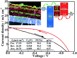
Metal phthalocyanines (MPcs) as an important class of organic semiconductors or hole transport materials (HTMs) have been extensively used in organic solar cells. Nevertheless, most of them are highly insoluble and need to be processed through a strict high-vacuum deposition process. Herein, a solution-processable tert-butyl substituted zinc phthalocyanine (hereafter referred to as ZnPc(tBu)4) with relatively high hole mobility and favorable HOMO and LUMO levels has been synthesized and employed as dopant-free HTM layer in methylammonium lead iodide (MAPbI3) perovskite solar cells (PSCs), and the corresponding ZnPc(tBu)4-based PSCs after optimizing the ZnPc(tBu)4 concentration achieved a power conversion efficiency (PCE) of 5.16% and 7.98% measured under forward and reverse voltage scanning, respectively. The unsatisfactory photovoltaic performance of ZnPc(tBu)4-based PSCs compared to the classical spiro-OMeTAD-based ones can be mainly due to the very low fill factor and severe hysteresis, which would be eliminated by further optimizing the device fabrication procedure and the interfacial contacts between the mesoporous TiO2 film and MAPbI3 overlayer, and thus the present solution-processable and dopant-free ZnPc(tBu)4 would be a potential substitute for the expensive HTMs containing multifold additives used in the current PSCs.


1 Introduction

The greenhouse effect and global warming have been caused by the increase in energy demand with fossil fuels. Compared with other energy resources, solar energy in all its useable forms is considered as the most promising energy source for the future. In order to harness the energy from the sun, a wide range of solar cells, such as silicon-based solar cells, organic photovoltaic cells (OPVs), dye-sensitized solar cells (DSSCs) and perovskite solar cells (PSCs), has been developed to convert the solar energy to electricity. Among which, PSCs fabricated by using organometal halide perovskites as light-absorber have attracted widespread attention due to their superior characteristics such as tunable direct bandgap over a wide range, high absorption coefficient, long electron–hole diffusion lengths, and relatively simple fabrication processes.1–4 In the past few years, the power conversion efficiency (PCE) of PSCs has exhibited an incredible rise, much quicker and more remarkable as compared to that offered by the conventional DSSCs.5–16

In 2009, Miyasaka's group has introduced perovskite as a light-absorber into the conventional liquid electrolyte-based DSSCs for the first time, it is a pity that the photovoltaic performance was highly unstable and deteriorated within a few minutes.5 Until 2012, real breakthrough occurred in the field of PSCs by using p-type solid-state hole transport materials (HTMs) instead of the liquid electrolyte.6,7 For instance, spiro-OMeTAD (2,2′,7,7′-tetrakis[N,N-di(4-methoxyphenyl)amino]-9,9′-spirobifluorene, a small molecule hole conductor) and PTAA (poly(triarylamine), a polymeric hole conductor) employed as the HTM layer of PSCs exhibited a PCE of 9.7% and 12.0%,6,7 respectively. Thereafter, a large number of researchers have been motivated to focus on the device architecture design,8 the composition optimization,9–11 the fabrication and post-processing of various functional layers.12–15 Right now, the state-of-the-art PCE of PSCs has been reported as high as ∼22%.16

Usually, an efficient PSC consists of perovskite light-absorber sandwiched between electron transport layer and hole transport layer. Although the hole transport layer is dispensable due to the ambipolar and long-range transport feature of perovskite, it is still important for the extraction and transportation of the photoexcited charge carriers so as to effectively retard the interfacial charge recombination.4 Depressingly, the most effective HTMs such as spiro-OMeTAD and PTAA suffered from the multiplex synthetic approaches and complicated purification processes. Moreover, those necessary dopants (such as lithium bis(tri-fluoromethanesulfonyl)imide (LiTFSI), 4-tert-butyl pyridine (t-BP), and cobalt complex) for enhancing the hole mobility usually induce a potential corrosion of the perovskite, and thus causing the instability of the whole device.17 All of these make PSCs to be very expensive and thus hinder its large scale application. Therefore, it is urgent to find cost-effective and stable alternative HTMs without corrosive additive. For this purpose, various small organic molecules,18–20 inorganic semi-conductors,21,22 and conjugated polymers23,24 have been explored as alternative HTMs for PSCs. However, very few of these new HTMs can reach the PCEs offered by the widely used spiro-OMeTAD.

Low-cost metal phthalocyanines (MPcs) with excellent thermal and chemical stability are easily synthesized and commonly used as sensitizers in DSSCs due to the intensive absorption in the UV/blue and the red/near-IR regions,25 or as p-type donors in OPVs due to the high hole mobility.26 Recently, Lianos' group has reported copper phthalocyanine (CuPc) as HTM layer of PSC and achieved a PCE of 5.0%.27 Thereafter, the same group used tetra-methyl substituted CuPc and subphthalocyanine as HTM layer of PSCs and achieved a PCE of 5.2% and 6.6%,28,29 respectively. Although these PCEs are very small as compared to that offered by other HTMs such as spiro-OMeTAD and PTAA, it leaves a lot of space for improvement by adjusting the hole transport properties through molecular modification and structure optimization.29 For instance, a PSC fabricated by using CuPc nanorods as HTM and carbon as counter electrode achieved both an improved PCE (16.1%) and an enhanced stability as compared to the spiro-OMeTAD-based device.30 Nevertheless, those CuPc-based HTM layers have to be deposited by evaporation process under a strict high-vacuum condition, which not only increases the fabrication cost but also limits the scope of application. To overcome these drawbacks, large steric hindrance units were introduced at the peripheral sites of MPc macrocycles, which can not only suppress the molecular aggregation, but also improve the inherent poor solubility for the utilization of solution-processing.31 For instance, a solution spin-coating process was used to prepare Zn(II)octa(2,6-diphenylphenoxy)phthalocyanine (TT80) layer as HTM of PSC and achieved a PCE of 2.6%, which was further improved to 6.7% by incorporating LiTFSI and t-BP as dopants.32 It demonstrated a route to low-cost solution-processing of MPc as HTM layer for PSCs by engineering new MPc systems. Very recently, Sfyri and co-workers reported a soluble n-butyl substituted-CuPc as HTM for PSC showed better performance with 8.5% PCE compared with tert-butyl substituted-CuPc due to its better molecular packing and conductivity, also indicating that alkyl chain substitution plays an important role on the conductivity of MPc HTM materials.33

Herein, a symmetrically tert-butyl substituted zinc(II)phthalo-cyanine (ZnPc(tBu)4) has been synthesized and used as alternative HTM in methylammonium lead iodide (MAPbI3)-based PSCs, in which ZnPc(tBu)4 chlorobenzene solution was spin-coated on MAPbI3 layer under ambient atmosphere (humidity: 30–70%) to form dopant-free HTM layer. Spectroscopic and electrochemical measurements showed that ZnPc(tBu)4 has suitable HOMO–LUMO level position, in favour of extraction and transportation of the photoexcited charge carriers that were verified by photo-luminescence (PL) and time-resolved photoluminescence (TRPL) spectra. After optimizing the ZnPc(tBu)4 concentration, the best performing ZnPc(tBu)4-based PSC without dopant achieved a PCE of 5.16% and 7.98% measured under forward and reverse voltage scanning (AM1.5G standard condition), respectively. For comparison, PSCs with spiro-OMeTAD as HTM layer was fabricated in the same condition and exhibited a PCE of 6.19% and 7.72% measured under forward and reverse voltage scanning, respectively. Moreover, the corresponding values were further enhanced to 9.88% and 10.88% by incorporating LiTFSI and t-BP in spiro-OMeTAD layer. All those PSCs fabricated with ZnPc(tBu)4 or spiro-OMeTAD as HTM layer suffered from similar low fill factor and severe hysteresis mainly due to the poor coverage of MAPbI3 overlayer on the mesoporous (mp) TiO2 film and the resulting undesirable interfacial contacts, which can be eliminated by further optimizing the device fabrication procedure, and thus the present solution-processable and dopant-free ZnPc(tBu)4 is a potential cost-effective and stable alternative HTM for low-cost PSCs.

2 Experimental section

2.1 Material preparation

PbI2 was purchased from Heptachroma Co, Ltd. Spiro-OMeTAD (2,2′,7,7′-tetrakis-(N,N-di-p-methoxyphenyl-amine)-9,9′-spirobifluorene) was purchased from Shenzhen Feiming Science and Technology Co, Ltd. All other analytical grade chemicals were purchased from Sinopharm Chemical Reagent Co. Ltd without purification unless otherwise noted.

CH3NH3I (MAI) was synthesized according to a procedure reported previously.2 Typically, 24 mL of methylamine solution in anhydrous ethanol (27–32 wt%), 10 mL of 57 wt% hydroiodic acid in water and 100 mL of anhydrous ethanol were mixed in a round bottom flack (200 mL) in an ice bath under magnetic stirring for 2 h, and then the solvent and the excess CH3NH2 were removed by evaporating. The resulted MAI product was dissolved in ethanol followed by recrystallized in diethyl ether under magnetic stirring for 30 min. This process was repeated three times and then dried at 60 °C in a vacuum oven for 12 h. ZnPc(tBu)4 was prepared in our laboratory according to a one-step synthetic route with inexpensive starting materials as shown in Fig. S1. 1H NMR (CDCl3, 300 MHz): δ = 8.9–8.4 (m, 8H), 7.8–8.1 (m, 4H), 1.75 ppm (s, 36H); TOF-MS (m/z) calcd for C48H48N8Zn [M + H]+ 801.9, found 800.24 (Fig. S2).

TiO2 paste was prepared by using home-made anatase TiO2 nanoparticles, which were synthesized as follows: 10 mL of tetra-butyl ortho-titanate (TBOT) was added into a mix solvent containing 2 mL of distilled water and 8 mL of anhydrous ethanol in a Teflon-lined autoclave (50 mL), which then kept at 180 °C for 24 h. After cooling down to room temperature, the precipitate was centrifugally separated and washed with distilled water and anhydrous ethanol for several times and then dried at 70 °C in air. The as-synthesized TiO2 product was characterized to be pure anatase crystal phase (JCPDS no. 21-1272, as shown in Fig. S3a) with particle sizes in the range of 10–20 nm centered at ∼12 nm (as observed from Fig. S3b).

2.2 Film and device fabrication

FTO glasses were cleaned with detergent, rinsed with water several times, then followed by ultrasonication in acetone, 2-propanol and ethanol successively for 15 min and dried by air, finally subjected to an O3/ultraviolet treatment for 30 min. A compact TiO2 (cp-TiO2) thin layer was deposited on the FTO substrate by spin coating a mildly acidic solution of titanium isopropoxide in 2-propanol at 3000 rpm for 45 s, subsequently annealed at 125 °C for 5 min and then 500 °C for 30 min. After cooling down to room temperature, the above nanosized anatase TiO2 paste was spin-coated on the cp-TiO2 layer at 3000 rpm for 45 s, and gradually sintered at 500 °C for 30 min in air. The resultant mesoporous TiO2 (mp-TiO2) film was treated in 40 mM TiCl4 solution for 30 min at 70 °C, and then rinsed with water and ethanol followed by sintering at 500 °C for 30 min.

Methylammonium lead iodide (MAPbI3) overlayer on mp-TiO2 film was fabricated through a modified sequential deposition method. 1.0 M PbI2 dimethylformamide solution (maintained at 70 °C) was spin-coated on the mp-TiO2 film at 3000 rpm for 30 s and heated at 90 °C on a hotplate in air for 5 min. After cooling down to room temperature, the same process was repeated again. For the formation of MAPbI3, the film loaded with PbI2 was dipped into 10 mg mL−1 MAI 2-propanol solution for 30 min, and then rinsed with 2-propanol and dried at 70 °C for 30 min. ZnPc(tBu)4 as HTM layer was spin-coated on the above MAPbI3 overlayer at 2500 rpm for 30 s by using dopant-free ZnPc(tBu)4 chlorobenzene solution with different concentrations. Regarding the deposition of spiro-OMeTAD layer without dopant, 5.9 × 10⁻² M chlorobenzene solution was used through the same processes, while the spiro-OMeTAD layer with dopants was spin-coated by using 5.9 × 10⁻² M chlorobenzene solution containing 17.5 mL of lithium bis(trifluoro-methylsulphonyl)imide (LiTFSI, J&K Chemical) and 28.8 mL of 4-tert-butylpyridine (t-BP, Sigma-Aldrich) acetonitrile solution (520 mg mL−1). Finally, a thin Au-layer was deposited on the HTM layer to form the counter electrode through a thermal evaporation process.

2.3 Material characterization

X-ray diffraction (XRD) measurements were performed on a Miniflex 600 X-ray diffractometer with Cu Kα irradiation (λ = 0.154 nm) at 40 kV and 15 mA and a scan rate of 4° min−1 in the range of 10° ≤ 2θ ≤ 50°. The surface and cross-section morphologies of the films were investigated by a field emission scanning electron microscope (FESEM, Zeiss Sigma). UV-vis diffuse reflectance absorption spectra (DRS) were obtained by a Shimadzu UV-3600 spectrophotometer equipped with an integrating sphere. UV-vis absorption spectra of ZnPc(tBu)4 solution were recorded on a TU-1810 spectrophotometer. Photoluminescence (PL) spectra were determined by a K2 ISIS spectrometer. Time-resolved photo-luminescence spectra (TRPL) were obtained on FES 920 fluorescence spectrophotometer (Edinburgh Instruments) with excitation wavelength of 377 nm and detection wavelength of 783 nm. Electrochemical measurements were carried out with a BAS CV-50 W voltammetric analyzer as described in our previous report.33 1H NMR spectra were recorded on a 300 MHz Bruker DPX 300 spectrometer in CDCl3. MALDI-TOF-MS spectra were taken on a Bruker BIFLEX III ultrahigh resolution Fourier transform ion cyclotron resonance (FT-ICR) mass spectrometer with alpha-cyano-4-hydroxycinnamic acid as a matrix.

The devices were illuminated by a 300 W solar simulator (Newport, 91160) with a power density of 100 mW cm−2 (AM1.5G simulated irradiation). The light intensity was determined using a reference monocrystalline silicon cell system (Oriel, U.S.). A Computer-controlled Keithley 2400 Sourcemeter was employed to collect the photocurrent–voltage (JV) curves of perovskite solar cells. The incident photon-to-electron conversion efficiency (IPCE) was measured by using a Model QE/IPCE system (PV Measurements Inc.). For the photoinduced open-circuit voltage decay (OCVD) measurements, the illumination was turned off using a shutter after the cell was first illuminated to a steady voltage, and then the OCVD curve was recorded. The above measurements were carried out on a CHI-604C electrochemical analyzer.

3 Results and discussion

The molecular structure of ZnPc(tBu)4 was showed in Fig. 1a, and its synthetic route and MALDI-TOF mass spectrum were provided in Fig. S1 and S2. The substitution of tert-butyl groups at the peripheral sites of ZnPc macrocycle can not only adjust the electronic properties and the energy band levels, but also effectively improve its solubility.32 In contrast to the unsubstituted ZnPc, ZnPc(tBu)4 exhibits much better solubility in various organic solvents, which benefits to the deposition of the HTM layer through solution spin-coating process that is more facile, economical and effective than the current evaporation process under a strict high-vacuum condition.30 The UV-vis absorption and PL spectra of 1.0 × 10⁻³ M ZnPc(tBu)4 dichloromethane (DCM) solution (Fig. 1b) indicate that ZnPc(tBu)4 has a maximum absorption in the red/near-IR region with two Q-band peaks at 610 and 678 nm in addition to a Soret-band absorption at 345 nm, while ZnPc(tBu)4 on mp-TiO2 film, that was made using a kind of anatase TiO2 nanoparticles (Fig. S3), exhibits a red-shift and dramatically broadened Q-bands due to the strong intermolecular π–π stacking effect (Fig. S4).32
image file: c6ra22451b-f1.tif
Fig. 1 (a) Molecular structure of ZnPc(tBu)4; (b) normalized UV-vis absorption and PL spectra of 1.0 × 10⁻³ M ZnPc(tBu)4 solution.

Fig. 1b also shows that ZnPc(tBu)4 has a maximum emission peak at ∼689 nm by exciting at 600 nm, and its optical bandgap (E0–0) can be estimated to be ∼1.82 eV from the intersection (λint = 683 nm) between the normalized absorption and emission spectra according to the previous reports.31,33 Cyclic voltammogram (CV) of ZnPc(tBu)4 shown in Fig. S5 was employed to investigate the electrochemical property, and the determined redox potentials as well as its calculated HOMO/LUMO levels are listed in Table 1. As can be seen, the HOMO of ZnPc(tBu)4 is calculated to be −5.31 eV, higher than the valence band (VB) level (−5.43 eV) of MAPbI3,5,6 indicating that the MAPbI3-to-ZnPc(tBu)4 hole transportation via the intimate interfacial contact is allowed thermodynamically.

Table 1 Calculated data of optical and electrochemical properties of ZnPc(tBu)4
Dye E1/2/V vs. SCE E0–0/eV HOMOa/eV LUMOb/eV
Ox Red
a Calculated with the equation EHOMO = −(Eox + 4.71) eV.b Calculated with the equation ELUMO = (EHOMO + E0–0) eV.
ZnPc(tBu)4 0.60 −1.00 1.82 −5.31 −3.49


PSCs were fabricated with a typical configuration of FTO/mp-TiO2/MAPbI3/HTM/Au as shown in Fig. 2a. The mp-TiO2 film plays the role of scaffold for supporting MAPbI3 and the electrons collector, and its thickness, porosity and particle size would greatly influence the device performance.34 Based on the above optical and electrochemical analysis results, a proposed energy band diagram of ZnPc(tBu)4-based PSC is shown in Fig. 2b. Under illumination, MAPbI3 can capture the incident photons and generate the charge carriers. Those photoexcited electrons can be transferred through the mp-TiO2 film and collected at FTO anode, while those holes are transported through the ZnPc(tBu)4 layer to Au cathode due to the appropriate alignments of those energy bands. In addition, the LUMO (−3.49 eV) of ZnPc(tBu)4 is higher than the conduction band (CB) level (−3.93 eV) of MAPbI3,6 implying that the transportation of those photoexcited electrons from MAPbI3 layer to Au cathode can be blocked, which benefits the directional transfer and separation of those photoexcited charge carriers of the MAPbI3 layer. In order to confirm the contribution of ZnPc(tBu)4 on the light harvesting, UV-vis diffuse reflectance absorption spectra (DRS) of FTO/mp-TiO2/MAPbI3 film after spin-coating ZnPc(tBu)4 or spiro-OMeTAD as HTM layer were measured and shown in Fig. 3. Although the spiro-OMeTAD layer can slightly improve the light absorption capacity of MAPbI3 film, the ZnPc(tBu)4 layer shows no any evident contribution on the light absorption possibly due to the very thin ZnPc(tBu)4 layer, which will be discussed below.


image file: c6ra22451b-f2.tif
Fig. 2 Schematic view (a) and energy band diagram (b) of the PSCs fabricated with spin-coated ZnPc(tBu)4 as HTM layer.

image file: c6ra22451b-f3.tif
Fig. 3 DRS spectra of FTO/mp-TiO2/MAPbI3 before and after spin-coating ZnPc(tBu)4 or spiro-OMeTAD as HTM layer.

The cross-section FESEM image (Fig. 4a) of the PSC fabricated with spin-coated ZnPc(tBu)4 layer reveals a well-defined layer-by-layer structure with clear interfaces. The thicknesses of cp-TiO2 layer, mp-TiO2 film infiltrated with MAPbI3, and Au layer are determined as approximately 60, 500, and 100 nm, respectively. A MAPbI3 capping layer with a thickness of ∼200 nm can also be clearly identified, but the spin-coated ZnPc(tBu)4 layer cannot be distinguished from the capping layer even though a thicker spiro-OMeTAD layer on MAPbI3 film can be observed from Fig. S6. It indicates that the ZnPc(tBu)4 layer is much thinner than the spiro-OMeTAD layer, which might be the reason that the ZnPc(tBu)4 layer shows no any evident contribution to the light absorption of MAPbI3 film (Fig. 3). Besides, the much thicker mp-TiO2 film (∼500 nm), as compared to that (∼200 nm) reported in the most efficient mp-TiO2 film-based PSCs,12,16 ought to provide enough space for the infiltration of PbI2 and MAI solutions, and thus the MAPbI3 would entirely formed in the porous structure of TiO2 film. Nevertheless, the clearly identified MAPbI3 capping layer with thickness of ∼200 nm (Fig. 4a) indicates that the porous structures of the present mp-TiO2 film are not favourable for the efficient infiltration of PbI2 and MAI solutions, and should be further optimized by selecting suitable TiO2 paste and/or mp-TiO2 film fabrication process.


image file: c6ra22451b-f4.tif
Fig. 4 (a) Cross-section FESEM image of the PSC with spin-coated ZnPc(tBu)4 layer (the scale bar is 200 nm); (b) XRD patterns of the FTO/mp-TiO2 films after spin-coating various components.

Fig. 4b depicts the XRD patterns of the FTO/mp-TiO2 films after spin-coating various components. It is evident that PbI2 can be effectively transformed to MAPbI3 by reacting with MAI solution as the appearance of new diffraction peaks ideally ascribable to the tetragonal perovskite MAPbI3.8 Nevertheless, a tiny XRD reflection near at 2θ = 12.9°, ascribable to the characteristic peak of PbI2, still can be observed. It indicates that a small amount of PbI2 is remained during the formation of MAPbI3 layer. Possibly, some PbI2 solution permeated inside the porous structures of mp-TiO2 film during the PbI2 deposition process, which retards the efficient contact with MAI solution, and causing the remained PbI2. Another possible reason for this issue might be the decomposition of the formed MAPbI3 since the present fabrication process was carried out under ambient atmosphere with a humidity range of 30–70%. It was reported that a certain amount of PbI2 residue has a passivation effect even though it is sensitive to the PbI2 content.35 After spin-coating ZnPc(tBu)4 or spiro-OMeTAD as HTM layer on FTO/mp-TiO2/MAPbI3 film, no new diffraction peak can be observed, indicating the stability of MAPbI3 during the HTM layer deposition process.

Fig. 5 presents the top-view FESEM images of the mp-TiO2 film and its spin-coated products with various components. As can be seen, mp-TiO2 film has porous structures (Fig. 5a). After the spin-coated PbI2 reacting with MAI solution, a MAPbI3 capping layer, composed of discrete crystals with varied and larger grain sizes in the range of 20–50 nm, are formed on mp-TiO2 film (Fig. 5b). Obviously, this MAPbI3 overlayer with some unfavourable characteristics such as too large porosity and high surface roughness possibly due to the unconstrained reaction between PbI2 and MAI in isopropanol and the ineffective MAPbI3 filling in the porous structures of mp-TiO2 film. This kind of MAPbI3 overlayer might lead to the unavoidable exposure of TiO2 film to the subsequently deposited HTM layer, and thus causing the deterioration of the device performance.36 After spin-coating ZnPc(tBu)4 layer, those evident defects of MAPbI3 layer can be compensated by a very thin ZnPc(tBu)4 continuous layer (Fig. 5c), which can act a blocking layer to facilitate the hole-extraction and prevent the electron leakage between TiO2 film and Au layer. However, this ZnPc(tBu)4 layer can also contact with the exposed TiO2 film through the voids of MAPbI3 layer, and thus causing the aggravation of charge recombination and then an unfavourable device performance,36 which will be further discussed below.


image file: c6ra22451b-f5.tif
Fig. 5 Top-view FE-SEM images of mp-TiO2 film (a), mp-TiO2/MAPbI3 film (b), and mp-TiO2/MAPbI3/ZnPc(tBu)4 (c). The scale bar is 200 nm.

A series of PSCs were fabricated under ambient condition, and their photovoltaic performances were characterized by current density–voltage (JV) measurements under simulated AM1.5G solar irradiation at 100 mW cm−2. As can be seen from Table 2, the PSC without HTM layer shows very poor PCE of 1.38% (measured under forward voltage scanning) with low short-circuit current density (Jsc), open-circuit voltage (Voc) and fill factor (FF), suggesting that the poor quality of the prepared MAPbI3 layer cannot efficiently extract and transport those photoexcited holes. Moreover, the direct contact between the Au cathode and the exposed mp-TiO2 film due to the incomplete coverage of MAPbI3 capping layer (Fig. 5b) also leads to serious electron leakage and charge recombination across the interfaces, and thus giving the low PCE.

Table 2 Photovoltaic characteristic parameters of PSCs fabricated with different HTM layers
HTMsa Jsc/mA cm−2 Voc/V FF/% η/%
a Data in parentheses are the concentration of ZnPc(tBu)4 or spiro-OMeTAD solution for the spin-coated HTM layer.b Spiro-OMeTAD solution containing t-BP and LiTFSI as dopants.
Without HTM layer 9.45 0.516 28.3 1.38
ZnPc(tBu)4 (2.5 × 10⁻³ M) 11.67 0.783 35.7 3.26
ZnPc(tBu)4 (5.0 × 10⁻³ M) 14.42 0.786 35.6 4.04
ZnPc(tBu)4 (1.0 × 10⁻² M) 17.19 0.879 34.1 5.16
ZnPc(tBu)4 (2.0 × 10⁻² M) 16.28 0.825 38.3 5.15
ZnPc(tBu)4 (2.5 × 10⁻² M) 11.58 0.898 35.4 3.68
Spiro-OMeTAD (5.9 × 10⁻² M) 16.61 0.895 41.6 6.19
Spiro-OMeTAD (5.9 × 10⁻² M)b 21.10 0.920 51.0 9.88


After spin-coating 2.5 × 10⁻³ M ZnPc(tBu)4 solution on MAPbI3 layer as HTM layer, the corresponding PSC shows significantly improved PCEs of 3.68% with enhanced Jsc, Voc and FF values. It suggests that ZnPc(tBu)4 layer can block the defects of MAPbI3 layer to prevent the electron leakage between the exposed TiO2 film and the Au cathode, and thus ZnPc(tBu)4 concentration was optimized for further improving the device performance. As can be seen from Table 2, the Jsc values exhibit a first increasing and then decreasing trend with a basically increasing Voc value upon enhancing ZnPc(tBu)4 concentration, and the PSC fabricated by spin-coating 1.0 × 10⁻² M ZnPc(tBu)4 solution as HTM layer achieved a maximum PCE of 5.16% with the highest Jsc value. Generally, a thicker HTM layer can be generated with enhancing ZnPc(tBu)4 concentration, and has a better blocking effect, while too thicker HTM layer also leads to more serious ZnPc(tBu)4 molecule aggregation that might cause the charge recombination, and thus the decreased Jsc value.31,37 Similarly, the dark current values of those ZnPc(tBu)4-based PSCs are lower than that of the PSC without HTM layer (Fig. S7), also confirming that the ZnPc(tBu)4 layer can act as a blocking layer to reduce the electron leakage and charge recombination. This reduction in dark current upon enhancing the ZnPc(tBu)4 concentration is also in agreement with the enhancement of Voc value (Table 2) since it was reported that a low dark current benefits to obtaining a high Voc of devices.38 The above results demonstrate that solution-processable and dopant-free ZnPc(tBu)4 would be a potential cost-effective HTM to efficiently facilitate the hole extraction in PSCs.

For comparison, spiro-OMeTAD-based PSCs with/without dopants were also fabricated under the same conditions. As can be seen from Table 2, the spiro-OMeTAD-based PSC exhibits a much better PCE of 6.19% than the ZnPc(tBu)4-based one, which can be further enhanced to 9.88% with higher Jsc, Voc and FF values by incorporating LiTFSI and t-BP as dopants. As mentioned above, the much thicker spiro-OMeTAD layer than the ZnPc(tBu)4 layer may have a better blocking effect, which can prevent the electron leakage more effectively to lower the dark current of the device (Fig. S7), and thus causing a better photovoltaic performance. Moreover, the spiro-OMeTAD-based PSC with dopants exhibits the lowest dark current due to the more effective charge extraction with improved charge conductivity, and this effective charge extraction can further decrease the carrier density within the perovskite layer, and then causing a reduced charge recombination rate.30

Fig. 6 depicts the monochromatic incident photon-to-electron conversion (IPCE) curves of the PSCs with various HTM layers, and the integrated photocurrent density for PSCs fabricated without HTM layer was calculated to be 10.6 mA cm−2, while the integrated photocurrent densities for PSCs fabricated with ZnPc(tBu)4 and spiro-OMeTAD as HTM layer were calculated to be 15.7 and 18.5 mA cm−2, respectively. As can be seen from the normalized IPCE values, both the dopant-free ZnPc(tBu)4 and the doped spiro-OMeTA as HTM layer can enhance the photocurrent density in the whole visible region (350–800 nm) due to their efficient blocking effect on the defects of perovskite layer, which can improve the charge collection. Once again, the doped spiro-OMeTA-based PSC exhibits a higher IPCE values than the dopant-free ZnPc(tBu)4-based one, consistent with their respective Jsc value as shown in Table 2. All those PSCs fabricated with both ZnPc(tBu)4 and spiro-OMeTAD as HTM layer suffered from similar low fill factor and severe hysteresis, and thus give very small PCEs as compared to that of the most efficient mp-TiO2 film-based PSCs.12,16


image file: c6ra22451b-f6.tif
Fig. 6 IPCE curves of the PSCs fabricated without HTM layer or with spin-coated ZnPc(tBu)4 and spiro-OMeTAD as HTM layer.

On the basis of the above physical characterization and discussions in the device architectures, the low fill factors of the present PSCs can mainly ascribed to the poor coverage of MAPbI3 layer on the mp-TiO2 film and the resulting undesirable interfacial contacts stemmed from our immature fabrication processes that were carried out in air without controlling the humidity. For instance, the thicker mp-TiO2 film composed of 10–20 nm nanoparticles might cause the unfavourable pore structures for efficient infiltration of MAPbI3 as-mentioned above, while the insufficient MAPbI3 coverage makes those exposed mp-TiO2 film become the possible charge recombination centers. On the other hand, the severe hystereses might also limit the improvement in PCEs for the present PSCs with ZnPc(tBu)4 or spiro-OMeTAD as HTM layer. As can be seen from Fig. 7, the doped spiro-OMeTAD-based PSC shows a hysteresis with an average PCE of 10.38%, in which the PCEs measured under forward and reverse voltage scanning (AM1.5 simulated irradiation) are 9.88% and 10.88%, respectively. Even more, the champion spin-coated dopant-free ZnPc(tBu)4-based PSC shows a more obvious hysteresis with PCEs of 5.16% and 7.98% under forward and reverse voltage scanning, respectively. Generally, the reverse voltage scanning gives higher Voc and FF than the forward one, and thus leads to a better device performance, consistent with the reported result.39 Even though the origin of hysteresis in photovoltaic characteristics of PSCs is still controversial,39–41 it was considered that the hysteresis is significantly dependent on the device structure, the methods for fabricating the perovskite and the contact materials. Possibly, the severe hysteresis in the present devices can be ascribed to the unfavorable MAPbI3 overlayer and interfacial contacts that result in poor interfacial charge transfer as mentioned above, and further work is needed to reduce or eliminate this hysteresis by optimizing the device fabrication procedure.


image file: c6ra22451b-f7.tif
Fig. 7 JV curves of the best-performing PSCs fabricated by using spin-coated ZnPc(tBu)4 (a) or spiro-OMeTAD with t-BP and LiTFSI dopants (b) layer measured under forward (black) and reverse (red) scanning with active area of 0.09 cm−2 (100 mW cm−2 simulated solar illumination). The insets are their respective photovoltaic parameters.

To evaluate the stability of those PSCs fabricated with dopant-free ZnPc(tBu)4 and doped spiro-OMeTAD as HTM layer, the corresponding unencapsulated devices were stored in dark under ambient conditions and measured for 120 h. The obtained results are shown in Fig. S8. As can be seen, the PCE of the dopant-free ZnPc(tBu)4-based PSC shows a decreasing trend at the first 30 h as that of the doped spiro-OMeTAD-based one, but it can increase and even reach the beginning value at 90 h while the doped spiro-OMeTAD-based PSC still kept a decreasing trend. After 120 h, the dopant-free ZnPc(tBu)4-based device maintains ∼85% PCE, while the doped spiro-OMeTAD-based one only kept 35% PCE. It is worthwhile to notice that the humidity is up to 70–80% during the device preparation and measurement, which is the main reason for the rapid decline in PCE of the doped spiro-OMeTAD-based one since the dopants are hygroscopic and water could accelerate the decomposition of the perovskite film.17,42

To further understand the charge recombination processes on the FTO/mp-TiO2/MAPbI3/HTM interfaces, the open-circuit voltage decay (OCVD) curves of PSCs fabricated with spin-coated ZnPc(tBu)4 or spiro-OMeTAD HTM layer were shown in Fig. 8. As can be seen from Fig. 8a, the decay trend of Voc value for the spiro-OMeTAD-based PSC is slower than that of the ZnPc(tBu)4-based one. It indicates that the spiro-OMeTAD layer can more effectively retard the charge recombination, which can be ascribed to the thicker spiro-OMeTAD layer than ZnPc(tBu)4 layer (Fig. 5 and S6) can more efficiently block the voids of MAPbI3 overlayer, and thus causing more efficient charge extraction. Also, the corresponding electrons lifetime (τn)–Voc curves (Fig. 8b) derived from the OCVD measurement indicates that the spiro-OMeTAD-based PSC has a relatively longer electrons lifetime than the ZnPc(tBu)4-based one, implying that spiro-OMeTAD as HTM layer could cause more efficient charge separation, and thus an improved photovoltaic performance as compared with ZnPc(tBu)4.38


image file: c6ra22451b-f8.tif
Fig. 8 Open-circuit voltage decay (OCVD) (a) and τnVoc (b) curves of the PSCs fabricated by spin-coating 1.0 × 10⁻² M ZnPc(tBu)4 or 5.9 × 10⁻² M spiro-OMeTAD solution containing t-BP and LiTFSI dopants as HTM layer.

The steady-state photoluminescence (PL) and time-resolved photoluminescence (TRPL) can be employed to compare the hole extraction capability of ZnPc(tBu)4 or spiro-OMeTAD layer.30 As shown in Fig. 9a, the PL emission peak arising from MAPbI3 can be significantly quenched by either dopant-free ZnPc(tBu)4 or doped spiro-OMeTAD layer, suggesting that the photoexcited holes can effectively transfer from the MAPbI3 layer to the HTM layer. The TRPL spectra (Fig. 9b) can further evaluate the hole-extraction rate, and also demonstrates that the dopant-free ZnPc(tBu)4 or the doped spiro-OMeTAD layer can accelerate the PL decay. Accordingly, it can be conjectured that the hole extraction capability is not the main reason for the evident gap in the photovoltaic performance between the dopant-free ZnPc(tBu)4-based and the doped spiro-OMeTAD-based PSCs, and the charge recombination would be mainly responsible for the performance difference, which can be validated from the above discussion on Fig. 8. Furthermore, the dopant-free ZnPc(tBu)4 layer displays a quenching effect comparable with the doped spiro-OMeTAD layer, confirming its potentiality as efficient HTM for low-cost PSCs.


image file: c6ra22451b-f9.tif
Fig. 9 PL quenching effect by the HTM layer spin-coated with 1.0 × 10⁻² M ZnPc(tBu)4 solution or 5.9 × 10⁻² M spiro-OMeTAD solution containing t-BP and LiTFSI dopants (a), and their time-resolved PL spectra at the peak emission wavelength (783 nm) with excited wavelength of 377 nm (b).

On the bases of the above experimental results and discussion, it can be concluded that the low PCEs of those PSCs fabricated with both ZnPc(tBu)4 and spiro-OMeTAD as HTM layer can be ascribed to their similar low fill factor and severe hysteresis mainly stemmed from the poor coverage of MAPbI3 layer on mp-TiO2 film and the resulting undesirable interfacial contacts, which can be eliminated by further optimizing the device fabrication procedure. Anyway, the present solution-processable and low-cost ZnPc(tBu)4 as dopant-free HTM layer of PSCs exhibits relatively high hole mobility and favourable HOMO and LUMO levels, and thus would be a potential cost-effective and stable HTMs for low-cost PSCs alternative to the current spiro-OMeTAD that is very expensive and usually need corrosive dopants for enhancing the hole mobility.

4 Conclusion

In summary, a solution-processable tert-butyl substituted zinc phthalocyanine (ZnPc(tBu)4) has been synthesized and employed as dopant-free HTM layer in MAPbI3-based perovskite solar cells (PSCs). The best performing ZnPc(tBu)4-based PSC achieved a power conversion efficiency (PCE) of 5.16% and 7.98% measured under forward and reverse voltage scanning, respectively. Although the present ZnPc(tBu)4-based PSCs exhibit lower PCEs than that offered by the classical spiro-OMeTAD-based ones for the moment, the major reasons for impeding the photovoltaic performance such as very low fill factor and severe hysteresis are mainly stemmed from the poor coverage of MAPbI3 layer on the mp-TiO2 film and the resulting undesirable interfacial contacts due to our immature device fabrication procedure. Nevertheless, the present ZnPc(tBu)4 as dopant-free HTM layer of PSCs exhibits relatively high hole mobility and favourable HOMO and LUMO levels very similar to the spiro-OMeTAD with dopants, and thus it can be concluded that solution-processable substituted zinc phthalocyanine would be a potential cost-effective, dopant-free and stable HTMs for low-cost PSCs by further modifying and engineering new MPc systems.

Acknowledgements

This work is supported by the Natural Science Foundation of China (21573166, 21271146 and 21271144), the Funds for Creative Research Groups of Hubei Province (2014CFA007), and Natural Science Foundation of Jiangsu Province (SBK2015020824) China.

Notes and references

  1. P. Gao, M. Grätzel and M. K. Nazeeruddin, Energy Environ. Sci., 2014, 7, 2448–2463 CAS.
  2. M. M. Lee, J. Teuscher, T. Miyasaka, T. N. Murakami and H. J. Snaith, Science, 2012, 338, 643–647 CrossRef CAS PubMed.
  3. S. D. Stranks, G. E. Eperon, G. Grancini, C. Menelaou, M. J. P. Alcocer, T. Leijtens, L. M. Herz, A. Petrozza and H. J. Snaith, Science, 2013, 342, 341–344 CrossRef CAS PubMed.
  4. A. Mei, X. Li, L. F. Liu, Z. L. Ku, T. F. Liu, Y. G. Rong, M. Xu, M. Hu, J. Z. Chen, Y. Yang, M. Grätzel and H. W. Han, Science, 2014, 345, 295–298 CrossRef CAS PubMed.
  5. A. Kojima, K. Teshima, Y. Shirai and T. Miyasaka, J. Am. Chem. Soc., 2009, 131, 6050–6051 CrossRef CAS PubMed.
  6. H. S. Kim, C. R. Lee, J. H. Im, K. B. Lee, T. Moehl, A. Marchioro, S. J. Moon, R. Humphry-Baker, J. H. Yum, J. E. Moser, M. Grätzel and N. G. Park, Sci. Rep., 2012, 2, 591–597 Search PubMed.
  7. J. H. Heo, S. H. Im, J. H. Noh, T. N. Mandal, C. S. Lim, J. A. Chang, Y. H. Lee, H.-J. Kim, A. Sarkar, M. K. Nazeeruddin, M. Grätzel and S. I. Seok, Nat. Photonics, 2013, 7, 486–491 CrossRef CAS.
  8. J. M. Ball, M. M. Lee, A. Hey and H. J. Snaith, Energy Environ. Sci., 2013, 6, 1739–1743 CAS.
  9. H. P. Zhou, Q. Chen, G. Li, S. Luo, T.-b. Song, H.-S. Duan, Z. R. Hong, J. B. You, Y. S. Liu and Y. Yang, Science, 2014, 345, 542–546 CrossRef CAS PubMed.
  10. N. J. Jeon, J. H. Noh, W. S. Yang, Y. C. Kim, S. Ryu, J. Seo and S. I. Seok, Nature, 2015, 517, 476–480 CrossRef CAS PubMed.
  11. W. S. Yang, J. H. Noh, N. J. Jeon, Y. C. Kim, S. Ryu, J. Seo and S. I. Seok, Science, 2015, 348, 1234–1237 CrossRef CAS PubMed.
  12. M. Z. Liu, M. B. Johnston and H. J. Snaith, Nature, 2013, 501, 395–398 CrossRef CAS PubMed.
  13. J. Burschka, N. Pellet, S. J. Moon, R. Humphry-Baker, P. Gao, M. K. Nazeeruddin and M. Gratzel, Nature, 2013, 499, 316–319 CrossRef CAS PubMed.
  14. N. J. Jeon, J. H. Noh, Y. C. Kim, W. S. Yang, S. Ryu and S. I. Seok, Nat. Mater., 2014, 13, 897–903 CrossRef CAS PubMed.
  15. W. Nie, H. Tsai, R. Asadpour, J.-C. Blancon, A. J. Neukirch, G. Gupta, J. J. Crochet, M. Chhowalla, S. Tretiak, M. A. Alam, H.-L. Wang and A. D. Mohite, Science, 2015, 347, 522–525 CrossRef CAS PubMed.
  16. http://www.nrel.gov/ncpv/images/efficiency_chart.jpg, accessed April 2016.
  17. J. Liu, Y. Z. Wu, C. J. Qin, X. D. Yang, T. Yasuda, A. Islam, K. Zhang, W. Q. Peng, W. Chen and L. Y. Han, Energy Environ. Sci., 2014, 7, 2963–2967 CAS.
  18. S. Kazim, F. J. Ramos, P. Gao, M. K. Nazeeruddin, M. Gratzel and S. Ahmad, Energy Environ. Sci., 2015, 8, 1816–1823 CAS.
  19. S. T. Lv, L. Y. Han, J. Y. Xiao, L. F. Zhu, J. J. Shi, H. Y. Wei, Y. Z. Xu, J. Dong, X. Xu, D. M. Li, S. R. Wang, Y. H. Luo, Q. B. Meng and X. G. Li, Chem. Commun., 2014, 50, 6931–6934 RSC.
  20. B. Xu, E. Sheibani, P. Liu, J. B. Zhang, H. N. Tian, N. Vlachopoulos, G. Boschloo, L. Kloo, A. Hagfeldt and L. C. Sun, Adv. Mater., 2014, 26, 6629–6634 CrossRef CAS PubMed.
  21. P. Qin, S. Tanaka, S. Ito, N. Tetreault, K. Manabe, H. Nishino, M. K. Nazeeruddin and M. Grätzel, Nat. Commun., 2014, 5, 3834 CAS.
  22. K. C. Wang, J. Y. Jeng, P. S. Shen, Y. C. Chang, E. W. Diau, C. H. Tsai, T. Y. Chao, H. C. Hsu, P. Y. Lin, P. Chen, T. F. Guo and T. C. Wen, Sci. Rep., 2014, 4, 4756–4763 Search PubMed.
  23. O. Malinkiewicz, A. Yella, Y. H. Lee, G. M. Espallargas, M. Graetzel, M. K. Nazeeruddin and H. J. Bolink, Nat. Photonics, 2013, 8, 128–132 CrossRef.
  24. B. Conings, L. Baeten, C. De Dobbelaere, J. D'Haen, J. Manca and H. G. Boyen, Adv. Mater., 2014, 26, 2041–2046 CrossRef CAS PubMed.
  25. M.-E. Ragoussi, J.-H. Yum, A. K. Chandiran, M. Ince, G. de la Torre, M. Grätzel, M. K. Nazeeruddin and T. Torres, ChemPhysChem, 2014, 15, 1033–1036 CrossRef CAS PubMed.
  26. S. Uchida, J. Xue, B. P. Rand and S. R. Forrest, Appl. Phys. Lett., 2004, 84, 4218–4220 CrossRef CAS.
  27. C. V. Kumar, G. Sfyri, D. Raptis, E. Stathatos and P. Lianos, RSC Adv., 2015, 5, 3786–3791 RSC.
  28. G. Sfyri, C. V. Kumar, G. abapathi, L. Giribabu, K. S. Andrikopoulos, E. Stathatos and P. Lianos, RSC Adv., 2015, 5, 69813–69818 RSC.
  29. G. Sfyri, C. V. Kumar, Y.-L. Wang, Z.-X. Xu, C. A. Krontiras and P. Lianos, Appl. Surf. Sci., 2016, 360, 767–771 CrossRef CAS.
  30. F. G. Zhang, X. C. Yang, M. Cheng, W. H. Wang and L. C. Sun, Nano Energy, 2016, 20, 108–116 CrossRef CAS.
  31. L. J. Yu, W. Y. Shi, L. Lin, Y. W. Liu, R. J. Li, T. Y. Peng and X. G. Li, Dalton Trans., 2014, 43, 8421–8430 RSC.
  32. F. Javier Ramos, M. Ince, M. Urbani, A. Abate, M. Gratzel, S. Ahmad, T. Torres and M. K. Nazeeruddin, Dalton Trans., 2015, 44, 10847–10851 RSC.
  33. G. Sfyri, Q. Chen, Y. W. Lin, Y. L. Wang, E. Nouri, Z. X. Xu and P. Lianos, Electrochim. Acta, 2016, 212, 929–933 CrossRef CAS.
  34. L. J. Yu, X. H. Zhang, C. S. Zhuang, L. Lin, R. J. Li and T. Y. Peng, Phys. Chem. Chem. Phys., 2014, 16, 4106–4114 RSC.
  35. S. D. Sung, D. P. Ojha, J. S. You, J. Lee, J. Kim and W. I. Lee, Nanoscale, 2015, 7, 8898–8906 RSC.
  36. Q. Chen, H. P. Zhou, T. B. Song, S. Luo, Z. Hong, H. S. Duan, L. Dou, Y. S. Liu and Y. Yang, Nano Lett., 2014, 14, 4158–4163 CrossRef CAS PubMed.
  37. G. J. Li, K. L. Ching, J. Y. L. Ho, M. Wong and H.-S. Kwok, Adv. Energy Mater., 2015, 5, 1401775 CrossRef.
  38. Z. L. Zhu, Y. Bai, T. Zhang, Z. K. Liu, X. Long, Z. H. Wei, Z. L. Wang, L. X. Zhang, J. N. Wang, F. Yan and S. H. Yang, Angew. Chem., 2014, 126, 12779–12783 CrossRef.
  39. J. L. Xu, K. Li, W. Y. Shi, R. J. Li and T. Y. Peng, J. Power Sources, 2014, 260, 233–242 CrossRef CAS.
  40. H. J. Snaith, A. Abate, J. M. Ball, G. E. Eperon, T. Leijtens, N. K. Noel, S. D. Stranks, J. T.-W. Wang, K. Wojciechowski and W. Zhang, J. Phys. Chem. Lett., 2014, 5, 1511–1515 CrossRef CAS PubMed.
  41. B. Wu, K. Fu, N. Yantara, G. Xing, S. Sun, T. C. Sum and N. Mathews, Adv. Energy Mater., 2015, 5, 1500829 CrossRef.
  42. X. Gong, M. Li, X. B. Shi, H. Ma, Z. K. Wang and L. S. Liao, Adv. Funct. Mater., 2015, 25, 6671 CrossRef CAS.

Footnote

Electronic supplementary information (ESI) available. See DOI: 10.1039/c6ra22451b

This journal is © The Royal Society of Chemistry 2016
Click here to see how this site uses Cookies. View our privacy policy here.