DOI:
10.1039/C6RA21424J
(Paper)
RSC Adv., 2016,
6, 107977-107983
Electron ballistic characteristic optimization in individual MWCNT by oxygen plasma treatment
Received
26th August 2016
, Accepted 12th October 2016
First published on 13th October 2016
Abstract
Surface treatment and bonding oxygen species represent a practical method for strongly enhancing the ballistic characteristic of carbon nanotubes (CNTs) because the electrical properties strongly depend on the surface states. In this work, oxygen plasma was introduced onto the CNTs to remove the remaining defects, leading to a 44.8% improvement in the graphite-like sp2 bonding, which represents the graphite level of the CNTs. Moreover, oxygen species were bonded onto each individual CNT, as seen from the AES analysis. The conductive characteristics, such as resistivity, electron concentration, and electron mobility, for individual treated CNTs were optimized significantly under 20 s oxygen plasma treatment, giving values of 1.23 × 10² μΩ cm, 6.36 × 1018 cm−3, and 8002.23 cm2 V−1 s−1, respectively. Furthermore, we demonstrated an experimental approach to grow aligned CNTs by substrate clamping configurations without a bias voltage or porous substrate, which simplifies the complexity of procedure preparation and enhances the opportunity for extracting individually treated CNTs to investigate their specific conductive characteristics.
1. Introduction
The miniaturization of electronic devices has been the principal driving force behind the semiconductor industry, and has brought major improvements in computational power and energy efficiency. Digital circuits based on transistors fabricated from carbon nanotubes (CNTs) have the potential to outperform silicon by improving the energy performance,1,2 due to their exceptional electronic and surface properties.3–9 The structural quality of the nanotubes coupled with the unique electrical properties of graphite means that the nanotubes are ballistic conductors and the electrons within the nanotubes move without resistance. Therefore, a perfect metallic nanotube is the best normal electron conductor. However, CNTs have, hitherto, been mostly used as supporting materials for catalytic nanoparticles or molecules,10–16 essentially to wire up more active conductive materials, unless they are modified or doped.17–20 There are many existing impurities that occur in the preparation process and with conjugated structures, which cause strong van der Waals interactions among the CNTs, so CNT-based composites often perform much worse than expected. Most of their applications, such as capacitive materials, and conductive characteristics are thwarted by this drawback.21 A considerable enhancement in the conductive performance of the CNTs has been achieved by combining them with metal oxides, such as Fe3O4,21 RuO2,22 and Co3O4;23 gas sources, such as nitrogen, i.e., by annealing pre-oxidized nanotubes in an NH3 environment;24 and by acid treatment by dip-coating in chlorosulfonic acid (CSA) solutions.25 By visualizing the oxygen plasma treatment at room temperature along with a pristine individual CNT, we herein show that it will, in fact, remove the defects from the CVD process and enhance the bonded oxygen species on the CNTs, resulting in an optimization of the conductive characteristics. The resistivity, electron concentration, and electron mobility for individually treated CNTs were improved significantly to 1.23 × 10² μΩ cm, 6.36 × 1018 cm−3, and 8002.23 cm2 V−1 s−1, respectively. Moreover, this work provides an experimental approach through substrate clamping configurations to grow aligned CNTs for extracting individual treated CNTs, which can be utilized in a specific conductive analysis.
2. Experimental
In this work, microwave plasma enhanced chemical vapor deposition (MPECVD) was used to synthesize multi-walled carbon nanotubes (MWCNTs), as shown in Fig. 1(a).19,20 An iron-containing compound was used as the catalyst, which was first coated onto a non-conductive silicon oxide substrate using a sol–gel method to promote the growth of the MWCNTs. The substrate was placed in the MPECVD chamber, where a mixture gas of methane and hydrogen (1![[thin space (1/6-em)]](https://www.rsc.org/images/entities/char_2009.gif) :10) was introduced and it was simultaneously decomposed by the microwaves to synthesize carbon-related materials. During this period, the pressure was kept at 20 Torr with a microwave power of 1.5 kW at 650 °C, as measured by a thermocouple (CA). In order to improve the CNTs' bundled mechanical properties, a substrate clamp mode was used to obtain aligned CNTs. Fig. 1(b) shows an illustration of the horizontal clamp substrate, showing how precursors were introduced onto the surface of the substrate indirectly. On the other hand, a vertical clamp substrate makes the precursors react with the catalyst directly, as shown in Fig. 1(c). After the growth of the CNTs, the microwave chamber was cooled down to room temperature, and surface modification treatment was subsequently started. The plasma treatments by different gas sources for the MWCNTs were conducted under the following conditions: oxygen gas flow rate, 20 sccm; operating pressure, 0.5 Torr; microwave power, 600 W; process duration, 5–35 s; and average sample temperature, about 30 °C.
:10) was introduced and it was simultaneously decomposed by the microwaves to synthesize carbon-related materials. During this period, the pressure was kept at 20 Torr with a microwave power of 1.5 kW at 650 °C, as measured by a thermocouple (CA). In order to improve the CNTs' bundled mechanical properties, a substrate clamp mode was used to obtain aligned CNTs. Fig. 1(b) shows an illustration of the horizontal clamp substrate, showing how precursors were introduced onto the surface of the substrate indirectly. On the other hand, a vertical clamp substrate makes the precursors react with the catalyst directly, as shown in Fig. 1(c). After the growth of the CNTs, the microwave chamber was cooled down to room temperature, and surface modification treatment was subsequently started. The plasma treatments by different gas sources for the MWCNTs were conducted under the following conditions: oxygen gas flow rate, 20 sccm; operating pressure, 0.5 Torr; microwave power, 600 W; process duration, 5–35 s; and average sample temperature, about 30 °C.
 |
| | Fig. 1 Illustration of (a) MPECVD systems, and the clamp substrate in the (b) Si horizontal sandwich approach and (c) Si vertical sandwich approach. | |
The morphology of the specimens was examined by field emission scanning electron microscopy (FE-SEM, JSM-6500F). High-resolution electron microscopy (HRTEM, JEOL JEM-2010) was performed at 200 kV with a point resolution of 0.19 nm and a lattice resolution of 0.1 nm. Chemical analysis of the treated CNTs was performed using X-ray photoelectron spectroscopy (XPS, Perkin Elmer model PHI 1600 system). The XPS spectra were recorded at the base pressure of 5 × 10⁻⁹ Torr using Mg K radiation (1253.6 eV) generated at a power of 250 W. An in situ 3 kV Ar+ ion gun was applied to sputter the samples. Energy calibration was completed using the C1s peak at 285 eV, with an energy resolution of 1.6 eV for the survey scan spectra and 0.2 eV for the core-level spectra. In order to determine the elemental composition change of the individual CNTs during the plasma treatments, auger electron spectroscopy (AES, ULVAC-PHI PHI-700) with a coaxial cylindrical mirror analyzer was applied to conduct a more exact analysis. A Schottky field emission electron source provided a high voltage electron beam (0.1–25 kV) with a diameter of less than 6 nm for secondary electron imaging. The energy resolution of the system was 0.5 eV, and the elemental detection limit was down to 0.01 at%. A four-probe nano-electronics measurement system FE-SEM (JEOL-7000F) was used to carry out the electrical measurements (Keithley, 4200), with a two-terminal configuration. For electrical characterization, the treated CNTs were removed from the original substrate in an ultrasonic bath of an acetone solution and were placed on a highly conductive Si(100) wafer coated with a 200 nm thick SiO2 insulating layer. This host substrate was patterned in advance with contact pads and markers. The markers were used to determine the exact position of the randomly disposed CNTs for the following electron beam lithography step. The CNTs were contacted individually with Al ohmic electrodes patterned by electron beam lithography.
3. Results and discussion
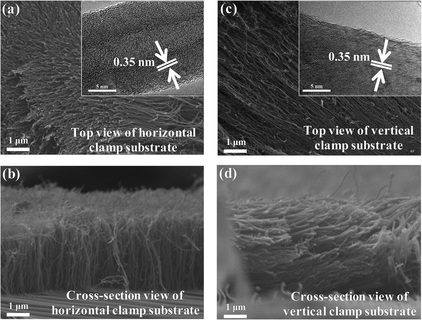
Fig. 2(a) shows the surface morphology of the CNTs grown by the horizontal clamp substrate method. A top view of the SEM showed that the CNTs seem to have an oncoming growth, while the corresponding HRTEM in Fig. 2(a) inset reveals a graphitic layer spacing of about 0.35 nm. As is clearly visible in the cross-sectional view of the SEM image in Fig. 2(b), CNTs grown straight on the Si substrate have a vertical length of about 4.2 μm, which resolves the bundled mechanical properties substantially in the CVD process. When the clamp substrate changes to the vertical position, the CNTs also maintain a certain growth direction, as shown in Fig. 2(c), and the graphitic layer spacing is 0.35 nm in the HRTEM inset. However, the growth direction is no longer perpendicular to the substrate, but instead grows along the substrate to form horizontal CNTs, as shown in Fig. 2(d). It can be concluded from these phenomena that a plasma gas source can be blocked by a Si horizontal substrate sandwich, and that CNTs are less affected by the precursors flow when grown perpendicular. On the other hand, a Si vertical substrate sandwich will be influenced directly to grow along with the substrate by a precursor flow introduced into the slit. This work provides an experimental approach to grow aligned CNTs without a bias voltage or porous substrate, which simplifies the complexity of the procedure preparation and enhances the opportunity for extracting individual CNTs in order to investigate their conductive characteristics. After the growth of the CNTs, surface oxygen plasma modification by different processes lasting 5–35 s was subsequently started.
 |
| | Fig. 2 SEM images of aligned (⊥) CNTs grown by the horizontal clamp substrate approach: (a) plane view, and inset shows the corresponding HRTEM image, (b) cross-sectional view. Aligned (//) CNTs grown by the vertical clamp substrate approach: (c) plane view, and inset shows the corresponding HRTEM image, (d) cross-sectional view. | |
The XPS survey spectra of group CNTs by oxygen plasma treatment, as seen in Fig. 3(a), show the presence of carbon and oxygen localized at 285 eV and 532.5 eV, respectively. These results clearly reveal that the oxygen-bonded carbon percentage can increase significantly with a longer plasma modification period, but it reaches a saturation value (∼19%) after 20 s treatment. In addition, it is important to analyze the chemical bonding signals by fine sweeping the specific atoms to investigate how the oxygen plasma treatment influences the bonding configuration of CNTs. Fig. 3(b) shows the C1s core-level spectrum under 20 s treatments, which can be decomposed into four components, as referred to in Marton et al.'s research.26 The carbon peak at the binding energy of 284.6 eV (1) was identified as free carbon, originating from adventitious carbon and surface carbon. The peak at C1: 285.9 eV (2) corresponds to the graphite-like sp2 carbon, which indicates the graphite level. The peak at 287.1 eV (3) can be attributed to the diamond-like sp3 carbon, which indicates the disorder level. The peaks at 288.3 (4) correspond to carboxyl (or ester) groups, respectively. All the peaks of the core-level spectra were fitted with the same value (1.3 eV) for the full width at half maximum. After the quantitative analysis, the relative percentages of the chemical bonding of the carbon atoms were recorded and are illustrated in Fig. 3(c). These results clearly reveal that the sp2 carbon has an obviously increasing trend from 0 to 20 s but becomes saturated at 35 s plasma treatment. However, the sp3 carbon has a smooth increasing status in the early period of treatment, but is then enhanced rapidly at 35 s. Therefore, the CNTs have a higher graphite level and less disorder at 20 s plasma treatment. These findings are in good agreement with those of our previous studies on modified-CNTs-based gas sensors19 and CZO heterostructures nanotubes.20 An appropriate oxygen plasma modification exerted on the surface of CNTs can thus not only remove impurities, such as vacancies, amorphous carbons, and non-reactive catalysts, by re-establishing carbon atoms on the graphene structure, but can also produce nanotube intramolecular junctions with a large surface adsorption area, which can strongly enhance the amount of bonded oxygen species.20 On the other hand, redundant ion bombardments may cause the creation of both dangling bonds and transient polygon carbon rings, such as octagons,20,27 thus enhancing sp3 bonding. Moreover, the carboxyl group bonding on the surface of CNTs can also be regarded as an indicator of an increased number of oxygen species,28 and this reaches its maximum percentage at 20 s plasma treatment. Free carbon is consumed with other chemical bonding, so the percentages decrease with the treatment time.
 |
| | Fig. 3 XPS spectra of MWCNTs treated by oxygen plasma for 0, 5, 20, and 35 s for (a) the survey spectra and (b) C1s peak fitting under 20 s oxygen plasma treatment. The brown line expresses the raw experimental data; pink line is the cumulative fitting curve similar to the raw experimental curve; black, red, green, and blue lines are the recommended fitting curves, while the binding energies of the recommended fitting peaks are listed in the inset, respectively. (c) The trend of different carbon bonding types. (d) Single nanotube component analysis by nano-auger for different oxygen plasma treatments. | |
The same trend is also observed in the AES survey spectra of individual modified CNTs, as illustrated in Fig. 3(d). The kinetic energies at 265 eV and 509 eV represent the elemental C and O auger peaks, respectively. The formation of these peaks indicate that oxygen has been bonded onto the surface of each individual CNT. Moreover, oxygen concentrations with various plasma treatment times of 0, 5, 20, and 35 s were calculated to be 0, 1.25, 4.25, and 4.2 atom%, respectively. This demonstrates that the oxygen concentration on the surface of CNTs is controllable by the plasma treatment time. However, the oxygen atomic percentage also reaches a saturation value when the treatment rises to 35 s, which was a comparable result with the XPS results. The variation of elemental compositions for group CNTs by XPS analysis and for individual CNTs by AES analysis are summarized in Table 1. These results conclude that sp2 bonding can be increased significantly to enhance oxygen bonding with carbon on the surface of the CNTs by plasma modification.
Table 1 Elemental compositions change for group and individual MWCNTs treated by oxygen plasma for 0, 5, 20, and 35 s. The relative percentage of the XPS four components of carbon atoms computed from Fig. 3
| Elemental composition change and XPS components of the carbon atoms |
| Condition |
Group MWCNTs and bonding components of carbon atoms by XPS |
Individual MWCNT by AES |
| C1s (%) |
O1s (%) |
C1: free carbon (%) |
C2: sp2 (%) |
C3: sp3 (%) |
C4: carboxyl (%) |
C (%) |
O (%) |
| 0 second |
94.22 |
5.78 |
78.87 |
15.41 |
3.78 |
1.96 |
100 |
0 |
| 5 seconds |
89.36 |
10.64 |
75.62 |
16.71 |
4.58 |
2.56 |
98.75 |
1.25 |
| 20 seconds |
80.44 |
19.56 |
68.64 |
22.32 |
5.24 |
3.32 |
95.75 |
4.25 |
| 35 seconds |
80.13 |
19.87 |
67.28 |
23.02 |
7.98 |
2.27 |
95.8 |
4.2 |
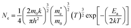
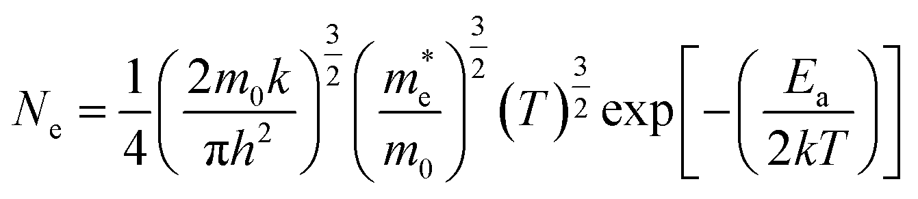
To investigate the electron transport properties of the treated CNTs junction system, we employed a four-probe FE-SEM system for performing electrical measurements at a single junction, which avoids the series or parallel problem of group CNTs. An individual CNT can be easily extracted from the original aligned CNT substrate in an acetone solution, which has lower bundled mechanical properties and placed on a highly conductive Si(100) wafer coated with a SiO2 insulating layer and Al electrodes. A single treated CNT was connected to two Al electrodes, as shown in the inset of Fig. 4(a), and the electrical behavior was measured. We investigated the I–V characteristics with a sweeping voltage ranging from −5 to 5 V. It is well known that the contact properties depend on the different work functions between the electrodes and the nanomaterial samples. When the work function of the contact metal is smaller than that of the nanomaterial, the conductive characteristic exhibits an ohmic contact.29 Because the work function of Al is about 4.28 eV, which is smaller than that of CNT of about 4.7 eV, a linear I–V curve of the treated CNT is obtained, as illustrated in Fig. 4(a), in which for the 0 and 5 s conditions, please refer to the left coordinates of Fig. 4(a); while for the 20 and 35 s conditions, please refer to right coordinates of Fig. 4(a). However, pristine and 5 s treated CNT exhibit semiconductor-like conductive properties, but in which the maximum current only reaches 5.67 × 10⁻² μA and 3.73 × 10⁻¹ μA, respectively. In contrast, the 20 s and 35 s treated CNTs provide typical metal-like conductive properties, and the maximum current can achieve 2.99 × 10² μA and 2.31 × 10² μA, respectively. The maximum tunneling current can be attained when the oxygen plasma was introduced at 20 s to the individual CNTs. Furthermore, resistivity values of 1.73 × 10⁵, 1.43 × 10⁵, 1.23 × 10², and 1.69 × 10² μΩ cm were found for individual CNTs with increasing the treatment time from 0, to 5, 20, and 35 s, respectively. These findings strongly suggest that the pristine CNT contains a high degree of impurities, which make it difficult to be a good electron transport channel, even if 5 s treatment is introduced, which is still insufficient. After increasing the oxygen treatment time to 20 s, the conductive characteristic are significantly improved. The numerically differentiated dI/dV curves in Fig. 4(b), in which for the 0 and 5 s conditions, please refer to the left coordinates of Fig. 4(b); while for the 20 and 35 s conditions, please refer to the right coordinates of Fig. 4(b), which are roughly proportional to the local density of states N(E) available for electrons tunneling from a four-probe FE-SEM system.30 The dI/dV data also indicate a distinct increase in these states as the nanotube is treated by oxygen. However, excessive treatment to 35 s will inhibit the conductive transmission, as suggested from the results of the analysis of the maximum current, resistivity, and density of states (DOS). In order to quantitatively analyze the treated CNTs specifically, the I–V curves were fitted by the Arrhenius equation:31,32
| |
 | (1) |
where
kTln(
ρ/
ρ0) gives the thermal activation energy
Ea = 256.27, 251.43, 70.11, and 78.29 meV for the 0, 5, 20, and 35 s treated CNTs, respectively. The electron concentration
Ne can be calculated by the equation shown below:
33,34| |
 | (2) |
where
m0 and

are the effective mass of an electron transmission in different band structures, but we can assume the difference is very small and can be neglected. The constant factor (1/4) × (2
m0k/π
h2)
3/2 has the value 4.84 × 10
15 (cm
−3 K
−3/2).
33,34 Thus, the electron concentration
Ne = 1.69 × 10
17, 1.86 × 10
17, 6.36 × 10
18, and 5.42 × 10
18 cm
−3 for the 0, 5, 20, and 35 s treated CNT can be acquired. Moreover, the specific sizes of the treated CNTs, including the length and diameter, can be directly obtained from the SEM and HRTEM images, respectively so that the electron mobility (
μ) is then computed by using the relationship:
| |
 | (3) |
where the values are 213.28, 234.37, 8002.23, and 6824.30 cm
2 V
−1 s
−1 for the 0, 5, 20, and 35 s treated CNTs, respectively. All the conductive characteristics for the individual treated CNTs are summarized in
Table 2.
 |
| | Fig. 4 (a) Four-probe FE-SEM system for electrical measurements at a single junction, comprising Al electrodes and isolated MWCNT treated by oxygen plasma for 0, 5, 20, and 35 s; inset shows the SEM image. (b) The corresponding dI/dV characteristics are roughly proportional to the local density of states N(E) available for electrons tunneling from the four-probe FE-SEM system. | |
Table 2 Electronic characteristics for individual CNTs treated by oxygen plasma
| Electronic characteristic for individual intramolecular junction nanotubes |
| Condition |
0 s |
5 s |
20 s |
35 s |
| Length (μm) |
8.33 |
3.19 |
4.63 |
4.39 |
| Area (cm2) |
1.61 × 10⁻¹² |
3.4 × 10⁻¹² |
3.4 × 10⁻¹² |
3.42 × 10⁻¹² |
| Max current (μA) |
5.67 × 10⁻² |
3.73 × 10⁻¹ |
2.99 × 10² |
2.31 × 10² |
| Resistivity: ρ (μΩ cm) |
1.73 × 10⁵ |
1.43 × 10⁵ |
1.23 × 10² |
1.69 × 10² |
| Activated energy Ea (meV) |
256.27 |
251.43 |
70.11 |
78.29 |
| Electron concentration: Ne (electron per cm3) |
1.69 × 10¹⁷ |
1.86 × 10¹⁷ |
6.36 × 10¹⁸ |
5.42 × 10¹⁸ |
| Electron mobility: μ (cm2 V−1 s−1) |
213.28 |
234.37 |
8002.23 |
6824.30 |
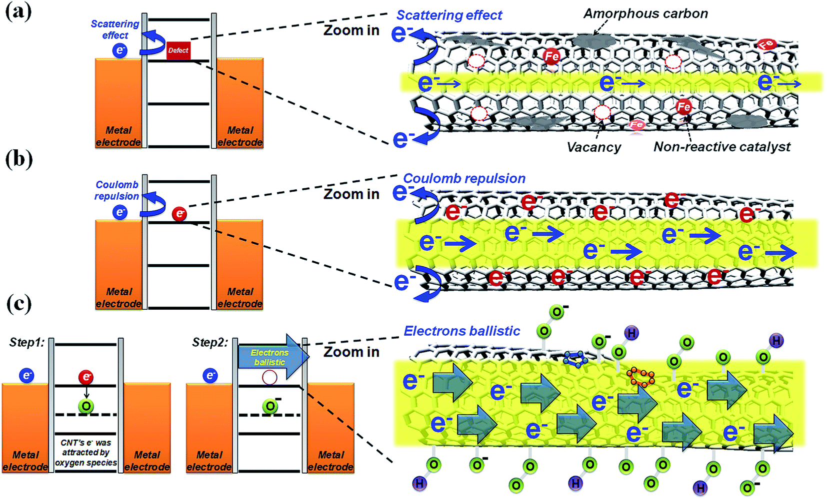
The variation of the conductive properties can be more concretely analyzed via a band diagram and mechanism, as illustrated in Fig. 5. Under different oxygen plasma treatment conditions, the electron transmission channel can be summarized by three phenomena: the first phenomenon is the pristine CNTs, which contain a large number of vacancies, amorphous carbons, and non-reactive catalysts.20 These defects will act as the scattering centers for transmitting electrons to inhibit conductive efficiency, as illustrated in Fig. 5(a). In the second phenomenon, after a rare oxygen plasma introduction, the surface defects of the CNTs are repaired gradually, but the transmitting electrons suffer coulomb blockage by the intrinsic electrons of CNTs, as shown in Fig. 5(b). An appropriate oxygen plasma treatment, however, not only removes the surface impurities of the CNTs, but also produces nanotube intramolecular junctions20 that strongly enhance the activation energy of the site and the surface adsorption area to allow more oxygen species to bond with the CNTs. Oxygen is known to have good charge transfer and high electronegativity characteristics, which will attract the intrinsic electrons of CNTs. Once the intrinsic electrons of CNTs are attracted, the transmitting electrons from the Al electrode will transfer ballistically, as shown in Fig. 5(c), which represents the final phenomenon. From the results reported above, it can be deduced that oxygen plasma treated CNTs could be highly useful in future nano-device applications.
 |
| | Fig. 5 Conduction mechanism for (a) pristine MWCNTs, (b) current blocked by coulomb repulsion for defect-free MWCNTs, and (c) electron ballistic tunneling in MWCNTs treated by oxygen plasma. | |
4. Conclusion
This work provides an experimental approach to grow aligned CNTs through applying different substrate clamping configurations without a bias voltage or porous substrate, which simplifies the complexity of the preparation procedure and enhances the opportunity for extracting individual treated CNTs in order to investigate their specific conductive characteristics. From the core-level XPS spectra analysis, it could be seen that the graphite-like sp2 bonding, representing the graphite level on the surface of the CNTs, could be improved 44.8% by oxygen plasma treatment. Furthermore, the formation of the peak from AES indicated that oxygen was bonded onto the surface of each individual CNT. After a quantitative analysis of the individual treated CNTs, the conductive parameters of the resistivity, electron concentration, and electron mobility were optimized significantly under 20 s oxygen plasma treatment and the values given were 1.23 × 10² μΩ cm, 6.36 × 1018 cm−3, and 8002.23 cm2 V−1 s−1, respectively. The mechanism was deduced whereby an appropriate oxygen plasma treatment not only removes the surface impurities of CNTs to avoid the scattering effect, but also produces more oxygen species bonded with carbon atoms, which can then attract the intrinsic electrons of the CNTs. Once the intrinsic electrons of the CNTs are fixed, the coulomb blockage effect can be eliminated and the transmitting electrons from the Al electrode can transfer ballistically. Therefore, oxygen plasma modified CNTs have wide potential for application with room temperature nanomaterial junction systems for devices and sensors.
Acknowledgements
This task was sponsored by the National Science Council of the Republic of China (Taiwan) under grant NSC-102-2221-E-034-003, NSC 102-2221-E-007-147-MY3, and NSC 102-2221-E-007-146-MY3.
References
- M. M. Shulaker, G. Hills, N. Patil, H. Wei, H. Y. Chen, H. S. P. Wong and S. Mitra, Nature, 2013, 501, 526 CrossRef CAS PubMed.
- A. D. Franklin, M. Luisier, S. J. Han, G. Tulevski, C. M. Breslin, L. Gignac, M. S. Lundstrom and W. Haensch, Nano Lett., 2012, 12, 758 CrossRef CAS PubMed.
- J. C. Byers, A. G. Güell and P. R. Unwin, J. Am. Chem. Soc., 2014, 136, 11252 CrossRef CAS PubMed.
- K. Balasubramanian and K. Kern, Adv. Mater., 2014, 26, 1154 CrossRef CAS PubMed.
- G. Wang, L. Zhang and J. Zhang, Chem. Soc. Rev., 2012, 41, 797 RSC.
- I. Dumitrescu, P. R. Unwin and J. V. Macpherson, Chem. Commun., 2009, 45, 6886 RSC.
- H. Wang, Y. Yuan, L. Wei, K. Goh, D. Yu and Y. Chen, Carbon, 2015, 81, 1 CrossRef CAS.
- X. Xu, H. Tan, K. Xi, S. Ding, D. Yu, S. Cheng, G. Yang, X. Peng, A. Fakeeh and R. V. Kumar, Carbon, 2015, 84, 491 CrossRef CAS.
- J. Qi, N. Benipal, D. J. Chadderdon, J. Huo, Y. Jiang, Y. Qiu, X. Han, Y. H. Hu, B. H. Shanks and W. Li, Carbon, 2015, 89, 142 CrossRef CAS.
- A. L. Goff, V. Artero, B. Jousselme, P. D. Tran, N. Guillet, R. Métayé, A. Fihri, S. Palacin and M. Fontecave, Science, 2009, 326, 1384 CrossRef PubMed.
- E. S. Andreiadis, P. A. Jacques, P. D. Tran, A. Leyris, M. C. Kerlidou, B. Jousselme, M. Matheron, J. Pécaut, S. Palacin, M. Fontecave and V. Artero, Nat. Chem., 2013, 5, 48 CrossRef CAS PubMed.
- A. Kongkanand, S. Kuwabata, G. Girishkumar and P. Kamat, Langmuir, 2006, 22, 2392 CrossRef CAS PubMed.
- S. Fu, G. Yang, Y. Zhou, H. B. Pan, C. M. Wai, D. Dua and Y. Lin, RSC Adv., 2015, 5, 32685 RSC.
- Z. Lu, X. Xiang, L. Zou and J. Xie, RSC Adv., 2015, 5, 42580 RSC.
- R. C. Pawar, S. Kang, S. H. Ahn and C. S. Lee, RSC Adv., 2015, 5, 24281 RSC.
- H. A. Park, S. Liu, P. A. Salvador, G. S. Rohrer and M. F. Islam, RSC Adv., 2016, 6, 22285 RSC.
- K. Gong, F. Du, Z. Xia, M. Durstock and L. Dai, Science, 2009, 323, 760 CrossRef CAS PubMed.
- Y. Li, W. Zhou, H. Wang, L. Xie, Y. Liang, F. Wei, J. C. Idrobo, S. J. Pennycook and H. Dai, Nat. Nanotechnol., 2012, 7, 394 CrossRef CAS PubMed.
- C. T. Hu, C. K. Liu, M. W. Huang, S. H. Syue, J. M. Wu, Y. S. Chang, J. W. Yeh and H. C. Shih, Diamond Relat. Mater., 2009, 18, 472 CrossRef CAS.
- C. T. Hu, J. W. Yeh and H. C. Shih, RSC Adv., 2016, 6, 60877 RSC.
- D. Guan, Z. Gao, W. Tang, J. Wang, Y. Yuan, B. Wang, M. Zhang and L. Liu, Mater. Sci. Eng., B, 2013, 178, 736 CrossRef CAS.
- R. R. Bi, X. L. Wu, F. F. Cao, L. Y. Jiang, Y. G. Guo and L. J. Wan, J. Phys. Chem. C, 2010, 114, 2448 CAS.
- J. Lang, X. Yan and Q. Xue, J. Power Sources, 2011, 196, 7841 CrossRef CAS.
- T. C. Nagaiah, S. Kundu, M. Bron, M. Muhler and W. Schuhmann, Electrochem. Commun., 2010, 12, 338 CrossRef CAS.
- F. Mirri, A. W. K. Ma, T. T. Hsu, N. Behabtu, S. L. Eichmann, C. C. Young, D. E. Tsentalovich and M. Pasquali, ACS Nano, 2012, 6, 9737 CrossRef CAS PubMed.
- D. Marton, K. J. Boyd, A. H. Al-Bayati, S. S. Todorov and J. W. Rabalais, Phys. Rev. Lett., 1994, 73, 118 CrossRef CAS PubMed.
- J. Niu, M. Li, W. Choi, L. Dai and Z. Xia, Carbon, 2014, 67, 627 CrossRef CAS.
- S. Banerjee and S. S. Wong, Nano Lett., 2002, 2, 195 CrossRef CAS.
- Z. Zhang, K. Yao, Y. Liu, C. Jin, X. Liang, Q. Chen and L. M. Peng, Adv. Funct. Mater., 2007, 17, 2478 CrossRef CAS.
- P. G. Collins, K. Bradley, M. Ishigami and A. Zettl, Science, 2000, 287, 1801 CrossRef CAS PubMed.
- C. G. Hu, W. L. Wang, K. J. Liao, G. B. Liu and Y. T. Wang, J. Phys. Chem. Solids, 2004, 65, 1731 CrossRef CAS.
- S. H. Syue, H. F. Kuo, C. T. Hsu, H. J. Chen, U. S. Chen, W. K. Hsu and H. C. Shih, Appl. Phys. Lett., 2008, 92, 232107 CrossRef.
- C. Kittel, Introduction to Solid State Physics, John Wiley & Sons, USA, 8th edn, 2005 Search PubMed.
- R. E. Hummel, Electronic Properties of Materials, Springer-Verlag, USA New York, 4th edn, 2011 Search PubMed.
|
| This journal is © The Royal Society of Chemistry 2016 |
Click here to see how this site uses Cookies. View our privacy policy here. 
 *a,
Jyh-Ming Wua,
Jien-Wei Yeha and
Han C. Shih*ab
*a,
Jyh-Ming Wua,
Jien-Wei Yeha and
Han C. Shih*ab


 are the effective mass of an electron transmission in different band structures, but we can assume the difference is very small and can be neglected. The constant factor (1/4) × (2 m0k/πh2)3/2 has the value 4.84 × 10¹⁵ (cm−3 K−3/2).33,34 Thus, the electron concentration Ne = 1.69 × 10¹⁷, 1.86 × 10¹⁷, 6.36 × 10¹⁸, and 5.42 × 1018 cm−3 for the 0, 5, 20, and 35 s treated CNT can be acquired. Moreover, the specific sizes of the treated CNTs, including the length and diameter, can be directly obtained from the SEM and HRTEM images, respectively so that the electron mobility (μ) is then computed by using the relationship: