
Anomalous red emission with competition and coexistence of defect and band edge emission in photo-electrochemically active (Zn0.97Ga0.03)(O0.95N0.05) solid solution†
Sumithra Sivadas Menona,
Sayantani Senb,
Pallabi Pramanikb,
Anirban Bhattacharyyac,
Bhavana Guptad,
Brajesh Tiwarie,
K. Baskaraf and
Shubra Singh*a
aCrystal Growth Centre, Anna University, Chennai – 600025, India. E-mail: shubra6@gmail.com
bCentre for Research in Nanoscience and Nanotechnology, University of Calcutta, Kolkata 700106, India
cInstitute of Radio Physics and Electronics, University of Calcutta, Kolkata 700009, India
dAccelerator & Nanoscience Group-Materials Science Group, Indira Gandhi Centre for Atomic Research, Kalpakkam 603102, India
eInstitute of Infrastructure Technology, Research and Management, Ahmedabad, Gujarat 380026, India
fManonmaniam Sundaranar University, Thirunelveli-627012, India
First published on 21st October 2016
Abstract
Photo-electrochemically active nanostructured (Zn0.97Ga0.03)(O0.95N0.05) solid solution has been synthesized by a solution combustion technique for realizing photocatalytic activity under visible light. A competing free excitonic and defect bound emission is observed from the sample which was investigated by temperature dependent photoluminescence from 4 K to 300 K. The defect bound emission dominates at room temperature providing an anomalous enhanced red emission, not reported before. A broad visible emission confirms the introduction of new defect levels as an impact of solid solution formation as established later by valence band (VB) XPS spectra. VB XPS shows the top of the valence band has shifted without affecting the conduction band, thereby reducing effective band gap of the solid solution from 3.35 eV to 2.8 eV. Tuning of the bandgap is essential to facilitate its activity under visible light irradiation as demonstrated in our present work. The generation of charge carriers, their effective separation and reduced trap states has been demonstrated by photoelectrochemical measurements in order to confirm the potential of the sample for efficient photocatalytic activity. The present sample exhibits a low mean life time with reduced trap states as compared to some previously reported results.
Introduction
The role of (oxy)nitrides for hydrogen evolution by photocatalytic water splitting has been widely researched in recent times due to their activity in the visible region of spectra.1a,b The catalytic properties of a catalyst are affected by the number of photoactive sites which in turn is directly proportional to the surface area of the catalyst. Hence it's crucial to develop nanoparticles with a large surface area to volume ratio to act as an efficient photocatalyst. (Ga1−xZnx)(N1−yOy), a d10 oxynitride solid solution has been investigated for its photocatalytic property with one step photo excitation, under visible irradiation and a reduced band gap compared to the parent materials.2 The reduction in band gap has been attributed to the repulsion between the Zn 3d and N 2p levels of valence band which shifts the valence band upwards, thereby reducing the band gap without affecting the conduction band.2a Studies have also found that short range orders have influence on electronic, atomic and vibrational properties of (Ga1−xZnx)(N1−yOy) and affects the band gap.2b The idea behind this solid solution formation is that it allows the intersubstitution of Zn/O ions by Ga/N ions which results in the introduction of new levels above the valence band affecting the band gap and hence the luminescence properties of the material.The fundamental nature of a photocatalyst can be investigated by a detailed analysis of the active surface sites and their role in the dynamics of adsorption and catalysis in molecular level. These measurements provide insight to electron transfer processes and active sites in the photocatalyst regardless of their morphology or porosity.3 A few research groups have tried to demonstrate the origin of visible light response of GaN–ZnO solid solution by employing photoluminescence studies. PL of GaN rich GaN–ZnO solid solution at 20 K only has revealed a yellow band at 570 nm (electronic transition from Ga vacancy to conduction band) and a blue band at 480 nm (electronic transition from Zn acceptor impurity to conduction band).4 Temperature-dependent photoluminescence (PL) and time-resolved photoluminescence (TRPL) for GaN rich (Ga1−xZnx)(N1−yOy) solid solution with x = 0.22 attributed the origin of luminescence to radiative recombination of donor bound electrons and acceptor bound holes.5 A detailed analysis of low temperature PL studies has not been reported yet for Zn(1−x)O(1−y)Ga(x)N(y) solid solution. This has motivated us to study the temperature dependent luminescence properties of nanostructured (Zn0.97Ga0.03)(O0.95N0.05) solid solution for a temperature range of 4–300 K and correlate it with the visible luminescence observed. The samples were synthesized by solution combustion method which is a much simpler low temperature technique as compared to the traditional high temperature nitridation method. Also, the reaction time is considerably reduced to less than 15 min (combustion technique) from 12 h (traditional nitridation technique) and the method doesn't involve any harmful by-products.
Experiment and characterization
For the preparation of the catalyst, zinc nitrate (99.9%), gallium nitrate (99.9%) and urea were used without further purification. Growth parameters and the starting metal molar ratio for the traditional combustion technique were optimized through various trial syntheses by varying molar ratio of urea/(Zn + Ga) as 3, 5 and 7, and Zn to Ga as 30, 40 and 50. It was found that when the ratio of urea/(Zn + Ga) is 3, the combustion was incomplete and when the ratio is 7, additional phases were formed. The chemical reaction was found to be complete when the urea/Zn + Ga ratio was 5 and Zn/Ga ratio was 50, yielding a sample with reduced band gap and higher Zn content. The required amount of metal nitrates and urea was dissolved in distilled water and stirred well until a clear solution was formed. It was then inserted into a muffle furnace maintained at a temperature of 500 °C. A vigorous reaction and combustion followed, forming fluffy, powder like samples with dark yellow color. The phase purity and structure of the solid solution was analyzed by powder X-ray diffraction (PXRD) technique, using PAN analytical X'Pert powder XRD system. Microstructural studies were performed by HRTEM (LIBRA 200 Carl Zeiss). Surface analysis such as core level spectra and valence band spectra was recorded using X-ray photoelectron spectroscopy (Omicron, Germany).Photoluminescence measurements on as synthesized samples were carried out with a helium–cadmium laser (325 nm) as the excitation source. The sample was mounted on to the cold finger of a Cryostat (Cryo Industries of America) and the temperature was varied from 4 K to 300 K. The temperature stability was better than 0.5 K at each measurement set-point. For the ultraviolet part of the spectrum, the light was dispersed using a 0.5 m monochromator with a 1200 lines per mm grating, and detected using a photomultiplier tube. The spectrum has been recorded from 340 nm. Since the band-gap of GaN is around 3.42 eV and that for ZnO is 3.37 eV at room temperature we have used a He–Cd laser for excitation which has sufficient energy, with its peak at 325 nm (3.81 eV), to create photogenerated carriers in the material. The photoluminescence spectrum has been recorded for the longer wavelengths, covering the range from ∼350 nm (3.54 eV) to about 800 nm. The wavelength region of 326 nm to 350 nm has been neglected due to scattering of the laser light from the sample, generating a scattered “laser tail”. However, since this wavelength region is far above the band-gap, no major spectral component from the sample is expected there. For the visible part of the luminescence, the Ocean Optics Jaz spectrometer was used.
Photoelectrochemical studies were carried out on spin coated (Zn0.97Ga0.03)(O0.95N0.05) thin film on ITO substrate. ITO/(Zn0.97Ga0.03)(O0.95N0.05) thin films were immersed in a 0.5 M Na2SO4 solution in a three necked quartz vessel with Pt as reference electrode and Ag/AgCl as the counter electrode and studies were made using Metrohm-Autolab model PGSTAT302N.
Results and discussions
Phase analysis carried out by powder XRD revealed single phase wurtzite structure with well defined diffraction peaks. Solution combustion technique synthesized (Zn0.97Ga0.03)(O0.95N0.05) solid solution shows diffraction peaks which are closer to that of ZnO, as is the case observed in Fig. 1a. The solid solution is observed only for certain optimized concentrations and the parent compounds do not form complete solid solutions. Presence of XRD peaks of (Zn0.97Ga0.03)(O0.95N0.05) solid solution between that of ZnO and GaN is attributed to the greater ionic radii of Zn2+ (0.74 Å) as compared to that of Ga3+ (0.55Å). A schematic presentation of wurtzite solid solution is presented in Fig. 1b. The crystalline size was calculated from XRD data and was found to be ∼40 nm using Scherrer formula.6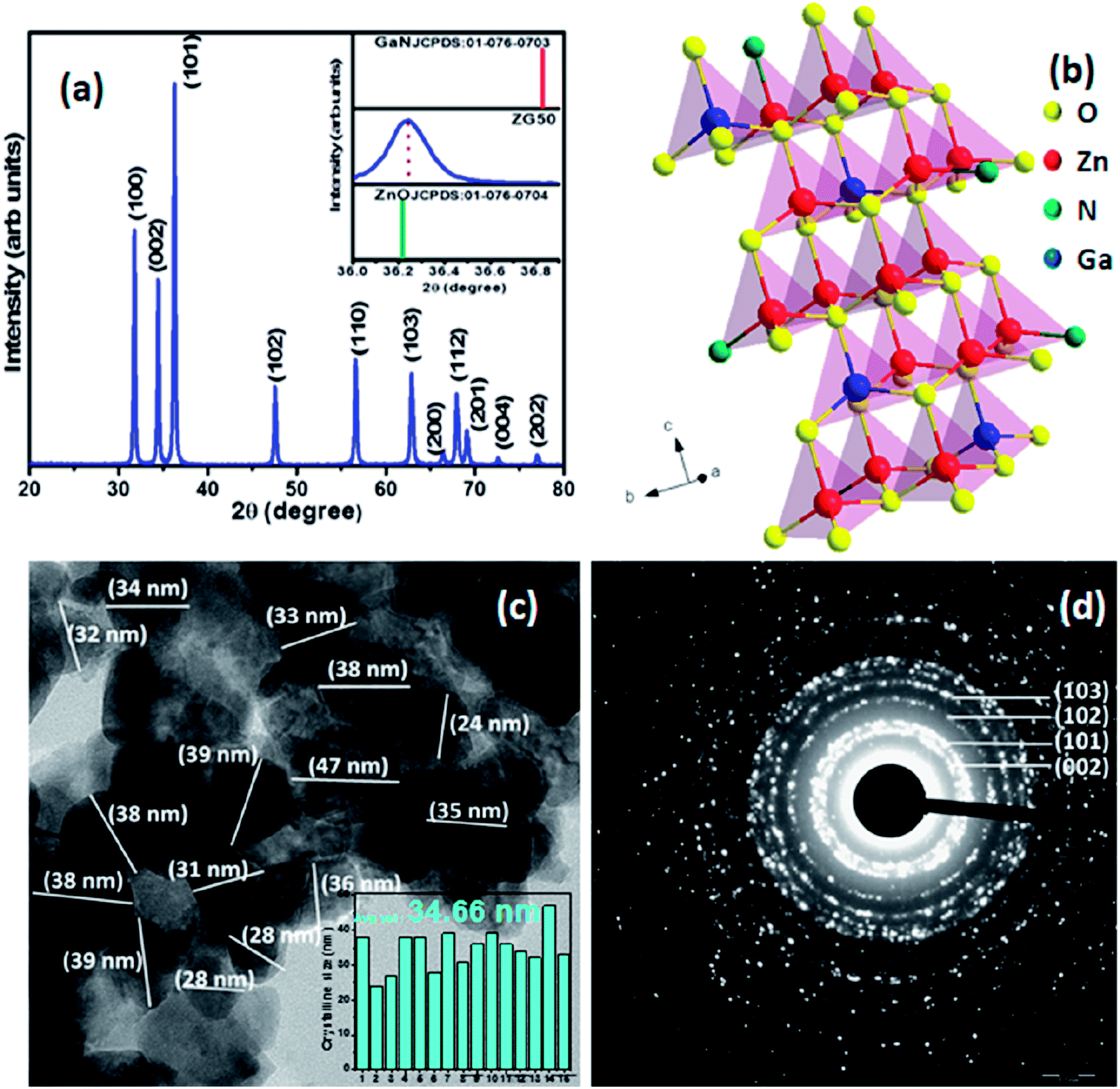 | ||
| Fig. 1 (a) XRD pattern of as prepared (Zn0.97Ga0.03)(O0.95N0.05) solid solution (inset: shift in (101) peak position of solid solution as compared to GaN and ZnO) (b) schematic representation of solid solution (c) particle size distribution of as prepared (Zn0.97Ga0.03)(O0.95N0.05) solid solution (inset: histogram of average crystalline size) (d) SAED pattern of the solid solution. | ||
The elemental presence and composition of sample were confirmed by EDAX and inductive coupled plasma (ICP), (ESI Table 1†). HRTEM images of the as prepared sample reveal particles with average diameter ∼34.6 nm (Fig. 1c) also corroborated by XRD data. The diffraction rings observed in the corresponding SAED pattern reveal the presence of (002), (101), (102) and (103) planes (Fig. 1d).
Substitution of Zn/O by Ga/N in the solid solution is bound to introduce new energy levels influencing the luminescence properties of the solid solution. The photoexcited active sites in metal oxide based photocatalysts could be well examined using low temperature PL providing an insight to the surface structures of oxides and their excited states so as to elucidate the mechanism of catalytic or photocatalytic behavior at molecular level. Hence, to investigate the impact of solid solution formation on luminescence of the parent material, temperature variant photoluminescence studies have been carried out from 4 K to 300 K. The temperature dependent spectra of near band edge (Fig. 2a) reveals two distinct emissions at 3.35 eV and 3.22 eV at low temperatures. At 4 K, the free exciton emission (FX) is observed at 3.36 eV, exhibiting a shift to lower energy with increase in temperature. The FX peak is prominent at temperatures below 100 K, broadening thereafter. The peak at 3.35 eV is assigned to donor bound excitons (D0X) which is the dominant emission at temperatures below 200 K. FX and D0X emissions are found to be mutually competitive. It is interesting to note that below 200 K the dominant emission at the near band edge is due to D0X, and as the temperature increases beyond 200 K, FX emission becomes prominent. As temperature increases, the intensities of D0X-related emissions decrease much faster than FX due to thermally activated donor-bound exciton.7 The emission at 3.28 eV is dominant at lower temperatures from 4 K to 200 K and flattens at room temperature. The energy dynamics of this emission is explained using the relationship
| E0 − Em = mΔhωLO − kBT, | (1) |
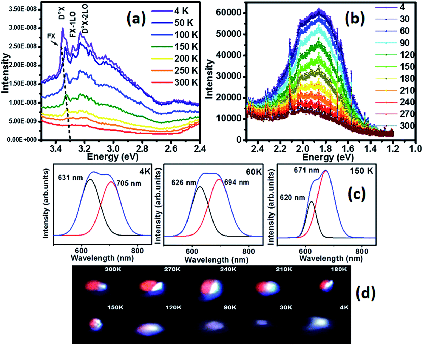 | ||
| Fig. 2 Low temperature photoluminescence of as prepared (Zn0.97Ga0.03)(O0.95N0.05) solid solution (a) near band edge emission (b) defect emission (c) deconvoluted PL peaks (d) snapshots of luminescence from the sample at different temperatures. | ||
Low temperatures encourage freezing of phonons as well as quenching of non-radiative recombination leading to an increase in emission intensity as well as shift in the peak position. The blue shift in DLE maximum with increase in temperature could be attributed to the populating of higher vibronic levels.13 Strong electron–phonon coupling in deep levels also give rise to a blue shift with increase in temperature.14 A similar blue shift of band edge emission with increasing temperature is caused by the thermal contraction of the lattice and changing electron–phonon interaction.15 When the temperature is less than 180 K there is no significant change in the peak position, but for higher temperatures there is a blue shift of peak maximum from 666 nm to 616 nm. Deconvolution of PL emission revealed the presence of a broad orange emission with two peaks around 631 nm and 705 nm at 4 K whose relative intensity changes with increase in temperature (Fig. 2c). The emission at higher wavelengths dominates at higher temperature and gives rise to an enhanced red colour of the illuminated sample. This enhanced red emission is captured at room temperature and is attributed to a combination of transitions involving native defects such as VO-Zni defect complex and VZnVO di-vacancies and an associated shallow donor (captured image, Fig. 2d). It is interesting to note that this red emission is suppressed at low temperature where near band edge emission predominates. As the temp decreases from room temperature a slow change is observed in the color emitted, from a red-violet to a prominent violet at extremely low temperatures. The intensity of emission in visible region is very high and enables us to witness it with naked eye and capture the same with camera coupled with spectrometer. To the best of our knowledge such an emission has not been observed before in related samples, suggesting creation of hybridized levels near VB and leading to effective narrowing of band gap.
XPS (Fig. 3a) analysis of the samples shows a broad and asymmetric N 1s peak centered at 398.65 eV with a full width at half maximum (FWHM) ∼4 eV suggesting the presence of more than one chemical state of nitrogen. Two peaks at 397.1 eV and 399.5 eV were identified by deconvolution. The peak at 399.5 eV suggests that the electron density on nitrogen remains similar to that of primary amines.16,17 The peak at 397.1 eV represents a Zn–N bond where N occupies oxygen vacancies in ZnO (VO) to form (N)O species contributing to deep acceptor levels and confirms N3− state of nitrides. It has been reported that the charge density of N in ZnO1−xNx is that of NH3 but an additional peak at 397 eV is observed with co doping of Ga and N which helps to form N3− state.18–20 The absence of any peak around 404 eV points to the fact that oxygen vacancy sites are not occupied by N2 forming (N2)O species. The Ga 2p doublet is observed at 1145.86 eV and 1119.16 eV ascertaining the presence of Ga3+ state as in GaN.19 XPS of Zn core level reveals the binding energies of the Zn 2p doublet at 1045.73 eV for 2p1/2 and 1022.82 eV for 2p3/2. The O 1s core level found at 531.3 eV is deconvoluted to reveal two peaks at 530 eV and 532.1 eV. The 530 eV peak corresponds to O in ZnO whereas the shoulder at 532.1 eV has been assigned to the oxygen in absorbed moisture on the sample whose binding energy lies between 531.5 eV and 535 eV.21
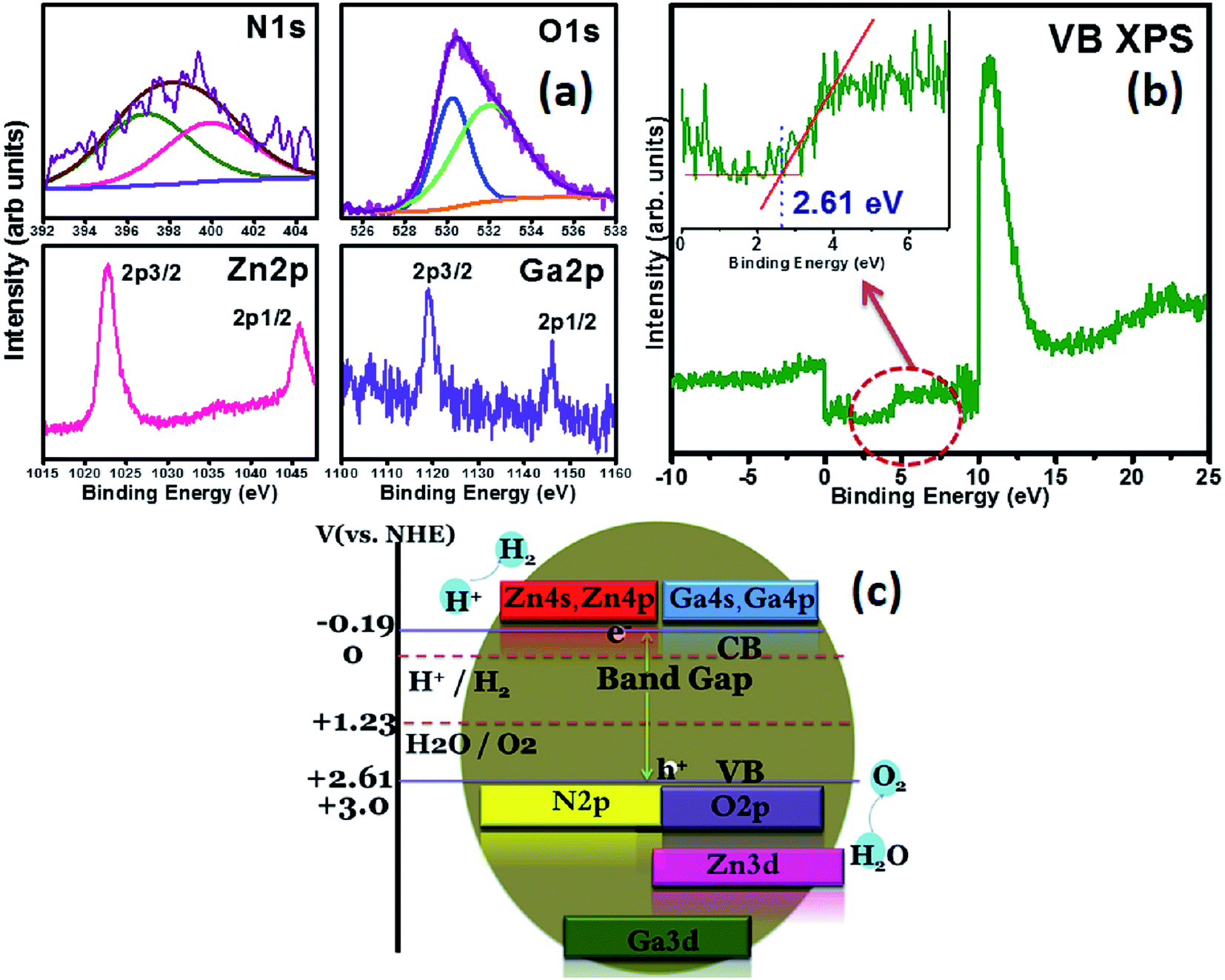 | ||
| Fig. 3 (a) Core level spectra of N 1s, O 2p, Zn 2p and Ga 2p (b) Valence Band (VB) spectra of the sample inset shows the valence band maximum energy (EVBmax) (c) schematic of electronic band structure of as synthesized sample. | ||
From the valence band XPS, several weak peaks were observed around Fermi level (EF) and a sharp peak of Zn 3d at 10.66 eV. The features observed in the energy range of 3–10 eV below Fermi level belong to O 2p states hybridizing with Zn 4s and Zn 4p.22 The position of valence band maximum (VBmax) is evaluated by taking linear extrapolation of the onset of XPS valence band spectra. A tangent to the fitted curve was drawn and the intercept is defined as VBmax.22 The value was found to be 2.61 eV indicating that the VB has shifted upwards, effectively reducing the band gap. This shift is attributed to the repulsion between the hybridized O 2p–Zn 2p bands and Zn 3d band. The band gap of the solid solution as found from diffuse reflectance spectroscopy (DRS) is found to be ∼2.8 eV (ESI Fig. 2†), thereby corroborating results from XPS studies. The conduction band minimum (CBmin) was obtained to be −0.19 eV since Eg = EVBmax(energy at valence band maximum) − ECBmin(energy at conduction band minimum), which is very close to that of reported value of ZnO (−0.2 eV), ascertaining that CBmin is unaffected during the solid solution formation and the observed reduction in band gap is due to the upshift of valence band.23 The conduction band is composed of Ga 4s, 4p and Zn 4s, 4p orbitals which undergo hybridization in the present case. There is no repulsion between the orbitals as in the case of p–d repulsion in valence band. Hence the position of conduction band minimum is unaffected. XPS analysis proves beyond doubt that the sample is infact a solid solution with an upshifted valence band.
Photocatalytic activity of the samples was realized using chronoamperometry, linear sweep voltammetry and impedance spectroscopy (Fig. 4).
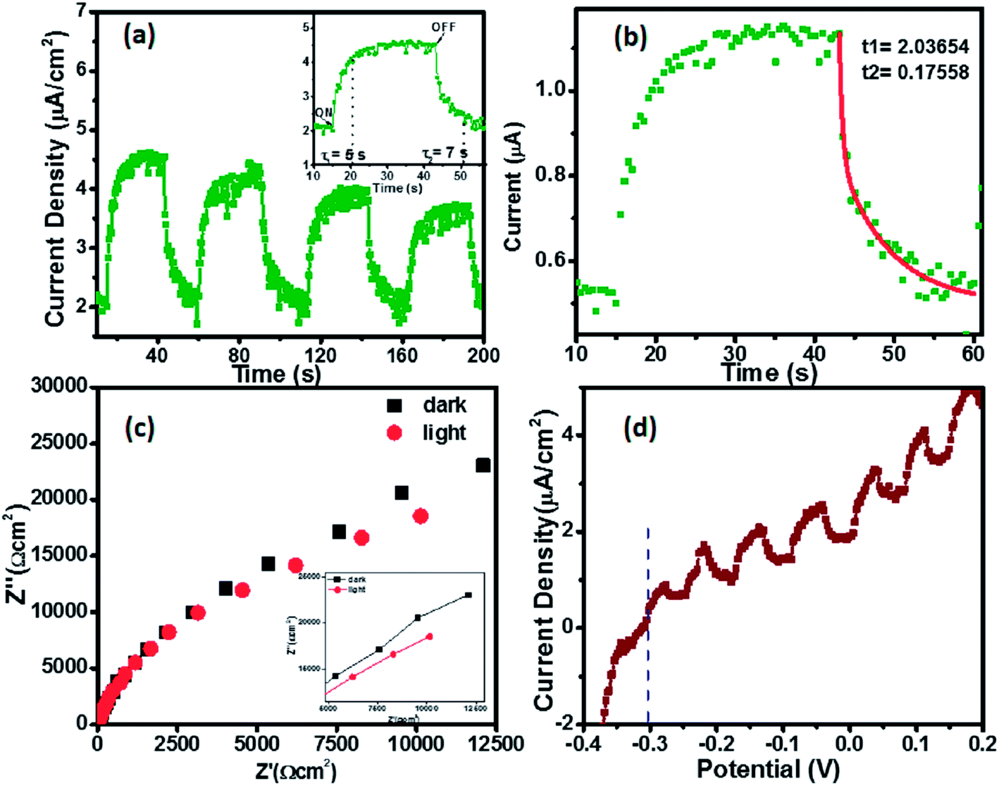 | ||
| Fig. 4 Plots representing photoelectrochemical measurements on (Zn0.97Ga0.03)(O0.95N0.05) films (a) chronoamperometry curve. Inset shows the current response for ON/OFF states (b) biexponential fitting to chronoamperometry curve (c) impedance measurement (inset shows magnified version) (d) linear sweep voltammetry measurements. | ||
A maximum photocurrent density of 4.5 μA cm−2 has been obtained under illumination as shown in Fig. 4a with the inset showing the response of current with light ON/OFF conditions. The response time and decay time was found to be 5 s and 7 s respectively. It is worth mentioning that the time constant for the rise time is always faster than the fall time, suggesting the involvement of traps and other defect states in this process. The decay observed in the current after each cycle indicates electron–hole recombination processes in the sample.24 The I–t curve has been used to fit a bi-exponential function with two time constants τ1 and τ2 as per the following equation
| Y(t) = Y0 + A1e−t/τ1 + A2e−t/τ2 | (2) |
| τm = τ1τ2/(τ1 + τ2) | (3) |
Linear sweep voltammetry was performed from −0.4 eV to 0.2 eV with a scan rate of 5 mV s−1 and a flat band potential at −310 meV vs. Ag/AgCl was observed. Impedance spectroscopic measurements under dark and light conditions on the sample show that the semicircular arc decreases under illumination. The results imply that efficient and rapid separation of photogenerated charge carriers takes place under light, validating the photocatalytic activity of as synthesized compound.26
Conclusion
In summary, nanostructured (Zn0.97Ga0.03)(O0.95N0.05) solid solution was synthesized by solution combustion technique and its defect and band edge emissions are investigated using temperature dependent photoluminescence. The phase pure sample has an effective band reduction from 3.35 eV to 2.8 eV due to the upshift of valence band. Our claim was supported by valence band XPS spectra where the valence band maximum was found to shift upwards. The samples exhibited an enhanced red luminescence at room temperature which gradually changed to violet luminescence as temperature was lowered from 300 K down to 4 K. The red emission and coexistence of defect and band edge emission is being reported for the first time for (Zn0.97Ga0.03)(O0.95N0.05) samples. The potential of the samples for photo-carrier generation under illumination has been demonstrated through photoelectrochemical studies, revealing the efficient generation and separation of charge carriers under visible illumination with an average current density of 4.5 μA cm−2.See ESI† for EDAX and diffuse reflectance spectroscopy data of the as prepared samples.
Acknowledgements
S. Singh would like to acknowledge the UGC-FRP scheme, DST-INSPIRE grant and DST Fast track young scientist program (SB/FTP/PS-023/2013). Pallabi Pramanik (09/028(0823)/2010-EMR-I) and Sayantani Sen (09/028(0921)/2014-EMR-I) would like to acknowledge the Council of Scientific and Industrial Research (CSIR) Senior Research Fellowship scheme.References
- (a) A. Fuertes, Mater. Horiz., 2015, 2, 453–461 RSC; (b) S. Martha, P. C. Sahoo and K. M. Parida, RSC Adv., 2015, 5, 61535–61553 RSC.
- (a) K. Maeda, T. Takata, M. Hara, N. Saito, Y. Inoue, H. Kobayashi and K. Domen, J. Am. Chem. Soc., 2005, 127, 8286–8287 CrossRef CAS PubMed; (b) J. Liu, M. V. Fernandez-Serra and P. B. Allen, Phys. Rev. B, 2016, 93, 054207 CrossRef.
- W. O. Haag, B. C. Gates and H. Knozinger, Adv. Catal., 1999, 44, 198–240 Search PubMed.
- M. Yoshida, T. Hirai, K. Maeda, N. Saito, J. Kubota, H. Kobayashi, Y. Inoue and K. Domen, J. Phys. Chem. C, 2010, 114, 15510–15515 CAS.
- Y. Lee, T. Lin, C. Wu, H. Teng, C. Hu, S. Hu and M. Yang, J. Appl. Phys., 2001, 109, 073506 CrossRef.
- A. L. Patterson, Phys. Rev., 1939, 56, 978–982 CrossRef CAS.
- B. Yan, R. Chen, W. Zhou, J. Zhang, H. Sun, H. Gong and T. Yu, Nanotechnology, 2010, 21, 445706–445712 CrossRef PubMed.
- W. Shan, W. Walukiewicz, J. W. Ager, K. M. Yu, H. B. Yuan, H. P. Xin, G. Cantwell and J. J. Song, Appl. Phys. Lett., 2005, 86, 191911 CrossRef.
- F. A. Kröger and H. J. Vink, J. Chem. Phys., 1954, 22, 250–252 CrossRef.
- M. Willander, O. Nur, J. Sadaf, M. IsrarQadir, S. Zaman, A. Zainelabdin, N. Bano and I. Hussain, Materials, 2010, 3, 2643–2667 CrossRef CAS.
- P. A. Rodnyi and I. V. Khodyuk, Opt. Spectrosc., 2011, 111, 776–785 CrossRef CAS.
- (a) X. Q. Wei, B. Y. Man, M. Liu, C. S. Xue, H. Z. Zhuang and C. Yang, Phys. B, 2007, 388, 145–152 CrossRef CAS; (b) Q. Ou, K. Shinj, A. Ogino and M. Nagatsu, J. Phys. D: Appl. Phys., 2008, 41, 205104–205109 CrossRef.
- S. L. Shi, G. Q. Li, S. J. Xu, Y. Zhao and G. H. Chen, J. Phys. Chem. B, 2006, 110, 10475–10478 CrossRef CAS PubMed.
- S. Singh, D. Nakamura, K. Sakai, T. Okada and M. S. R. Rao, New J. Phys., 2010, 12, 023007–023011 CrossRef.
- X. T. Zhang, Y. C. Liu, Z. Z. Zhi, J. Y. Zhang, Y. M. Lu, D. Z. Shen, W. Xu, X. W. Fan and X. G. Cong, J. Lumin., 2002, 99, 149–154 CrossRef CAS.
- V. Musat, A. M. Rego, R. Monteiro and E. Fortunato, Thin Solid Films, 2008, 516, 1512–1515 CrossRef CAS.
- M. Mapa, K. S. Thushara, B. Saha, P. Chakraborty, C. M. Janet, R. P. Viswanath, C. M. Nair, K. V. G. K. Murthy and C. S. Gopinath, Chem. Mater., 2009, 21, 2973–2979 CrossRef CAS.
- W. W. Liu, B. Yao, Z. Z. Zhang, Y. F. Li, B. H. Li, C. X. Shan, J. Y. Zhang, D. Z. Shen and X. W. Fan, J. Appl. Phys., 2011, 109, 093518 CrossRef.
- C. L. Perkins, S. H. Lee, X. Li, S. E. Asher and T. J. Coutts, J. Appl. Phys., 2005, 97, 034907 CrossRef.
- X. Zong, C. San, H. Yu, Z. G. Chen, Z. Xing, D. Ye, G. Q. Lu, X. Li and L. Wang, J. Phys. Chem. C, 2013, 117, 4937–4942 CAS.
- M. Mapa and C. S. Gopinath, Chem. Mater., 2009, 21, 351–359 CrossRef CAS.
- A. G. Joshi, S. Sahai, N. Gandhi, Y. G. R. Krishna and D. Haranath, Appl. Phys. Lett., 2010, 96, 123102 CrossRef.
- A. Janotti and C. G. Van de Walle, Rep. Prog. Phys., 2009, 72, 126501–126530 CrossRef.
- G. Cappelletti, V. Pifferi, S. Mostoni, L. Falciola, C. Di Bari, F. Spadavecchia, D. Meroni, E. Davoli and S. Ardizzone, Chem. Commun., 2015, 51, 10459–10462 RSC.
- Y.-C. Pu, G. Wang, K.-D. Chang, Y. Ling, Y.-K. Lin, B. C. Fitzmorris, C.-M. Liu, X. Lu, Y. Tong, J. Z. Zhang, Y.-J. Hsu and Y. Li, Nano Lett., 2003, 13, 3817–3823 CrossRef PubMed.
- B. Gupta, A. A. Melvin, T. Matthews, S. Dhara, S. Dash and A. K. Tyagi, Int. J. Hydrogen Energy, 2015, 40, 5815–5823 CrossRef CAS.
Footnote |
| † Electronic supplementary information (ESI) available. See DOI: 10.1039/c6ra21078c |
| This journal is © The Royal Society of Chemistry 2016 |