
Electronic, optical and vibrational features of BiVO4 nanostructures investigated by first-principles calculations
K. Ordonab,
A. Kassibab and
M. Makowska-Janusik*a
aInstitute of Physics, Faculty of Mathematics and Natural Science, Jan Dlugosz University in Czestochowa, Al. Armii Krajowej 13/5, 42200 Czestochowa, Poland. E-mail: m.makowska@ajd.czest.pl
bInstitute of Molecules and Materials of Le Mans, Université du Maine, 72085 Le Mans, France
First published on 7th November 2016
Abstract
Numerical models based on DFT and semi-empirical methods were developed on bulk and nano-sized BiVO4 semiconducting oxide. Two different approaches were implemented to calculate the electronic properties of the bulk BiVO4 crystal. One approach used the X-ray specified atomic positions with the defined lattice parameters involved in the monoclinic crystalline structure of BiVO4, for which geometry optimization was performed before the electronic properties calculations. The second approach considered the atomic positions of the scheelite structure, which was maintained frozen without any lattice rearrangement. The obtained data were considered as a guideline to choose appropriate methodology to calculate the physical properties of (BiVO4)n nanoparticles. A semi-empirical method with the PM6 parameterization was applied to calculate the electronic and vibrational properties of (BiVO4)n nanostructures versus their sizes. The quantum confinement effect was shown for the clusters through a blue-shift of the optical absorption bands compared to an infinite system. It was demonstrated that the optical and vibrational properties of the nanoparticles are determined by the internal atoms keeping their positions as in the crystalline structure and also that they feel surface reconstruction effects according to the environmental interactions. The above mentioned behaviors were analyzed (using UV-vis absorption, IR and Raman features), theoretically predicted and then compared with the experimental results. The performed analyses underlines the evolution of the electronic density of states and the optical absorption peculiarities between a bulk infinite system and nano-sized objects dedicated to realize visible-light-driven photocatalysts.
Introduction
Photocatalysis is a strongly expanding scientific area that can contribute to addressing a range of societal challenges, such as the need for new sources of energy and processes for environmental preservation, including the production of hydrogen from water dissociation, the degradation of organic pollutants from liquids and the atmosphere, as well as the development of self-cleaning surfaces. Additionally, the water-splitting process, which uses solar energy to generate hydrogen, is a promising way to produce renewable fuel. To date, the most commonly used photocatalysts have been based on titanium dioxide (TiO2)1 and have been extensively investigated during the last two decades. However, the high band gap of TiO2 (3.2 eV)2 limits the absorbed sunlight to only 6% of its UV spectral range. Therefore, the search for alternative visible-light-driven photocatalysts is an active quest and concerns a wide class of semiconducting oxides.Among the most promising structures, bismuth vanadate (BiVO4) is worthy of interest since it possesses many of the required features to compete with the already exploited photocatalysts.3 Moreover, BiVO4 nanostructures have attracted a broad interest due to their electrical, optical and mechanical properties. In particular, the use of BiVO4, with an energy gap equal to 2.3–2.4 eV,4,5 as a photocatalyst under solar light irradiation, was first reported by Kudo et al.,5–7 and it demonstrated good efficiency combined with chemical stability and nontoxicity. From structural aspect, three polytypes characterise the crystallography of BiVO4, which can be stabilized in monoclinic, tetragonal scheelite or zircon phases, however, only the monoclinic structure shows a low electronic band gap appropriate enough to harvest visible light irradiation8–10 as required for photocatalysis. However, the photocatalytic activity of pure BiVO4 remains limited due to the high recombination rate of photogenerated e−–h+ pairs and the fast charge carriers mobility. A suitable doping of the discussed structure by both metallic and non-metallic ions may help to improve the required photoactivity. This procedure was exhaustively carried out on X–BiVO4 systems, with X = N, Cu, Co, Fe, Mo or W.11–13 The photoactivity of the nanostructured BiVO4 was investigated in several situations,14 such as in nanocomposites based on Cu2O,15 Bi2O3,16 WO3,17 β-AgVO3,18 Bi2WO6 (ref. 19) and BiVO4.20–24 Also the versatility of the synthesis methods contributes to obtaine BiVO4 with different morphologies, such as thin films, mesoporous materials, powders, and nanostructures with different sizes and crystal order. Thus, monoclinic BiVO4 can be synthesised by a solid-state reaction,23–25 hydrothermal treatment,26,27 sonochemical method28 or by metal–organic decomposition.29
The photocatalytic properties of BiVO4 are intimately dependent on its electronic and optical peculiarities. These features are clearly a function of the stoichiometry, shape, size and the active exposed area. Though experimental procedures can modulate all these parameters, their effects on the electronic properties of the designed materials should be characterized and explained. Here, theoretical approaches supported by numerical analyses are able to evaluate the relevance and influence of each mentioned parameter and can allow better orienting the experimental investigations. Thus, in this work, we applied numerical modelling to predict and describe quantitatively the key physical properties of BiVO4 in its nano-sized forms. To the best of our knowledge, the cluster methodology that we developed in this work has not been considered up to now in the related literature. The implemented methodology and numerical analysis we used in the present study are based on the cluster model, which we also successfully applied to other classes of semiconducting oxides (titanium oxides, nickel titanate).30 Additionally, quantum-chemical calculations were implemented to explain the electronic properties of the studied nanoparticles with different sizes and to elucidate the influence of the surface effects on their electronic and vibrational properties. The developed approach is correlated with the former work on bulk BiVO4 structures and analysis of their electronic properties.31–40 Based on density functional theory (DFT) and applying the GGA/PBE potential, it has been shown that the largest contributions to the valence band maximum (VBM) are the O 2p and Bi 6s orbitals, while the conduction band minimum (CBM) is composed of V 3d orbitals.32,37,41–43 The energy band gap calculated for the monoclinic polytype of BiVO4 by using the DFT method gave values in the range of 2.1–2.6 eV.32,44
The present work combines the quantum-chemical calculations of the electronic and vibrational properties of BiVO4 nanoparticles versus their size, structural and surface features. The evaluations of the relevant properties of the nanostructures were then compared to the native bulk crystal features in order to highlight the major changes occurring with the size reduction and leading to structural relaxation. The calculations were performed by implementing a DFT methodology supported by a semi-empirical protocol based on a PM6 parameterized method. This theoretical approach applies to model the features of the mesoporous BiVO4 structure offering high specific surfaces that enhance the photocatalytic properties. The computationally obtained data predicted by the numerical simulations were combined with the experimental results, allowing a clearer evaluation of the related vibrational, electronic and optical features.
Computational methodology
Up to now, theoretical models supported by numerical simulations have been developed for bulk BiVO4 focusing on electronic band structures and density of states calculations for pure and doped systems.31–44 To the best of our knowledge, no studies have reported models of the nanocrystalline forms of the BiVO4 in contrast to reports on the bulk-like system. Therefore, we outline below our methodology based on theoretical models and numerical simulation analysis to predict the electronic and vibrational properties of nano-sized materials. First though, the bulk material properties were first simulated and are discussed herein. This step helps to orient the subsequent approach used to evaluate the electronic and vibration properties of the nano-sized BiVO4 structures.Bulk BiVO4 with monoclinic scheelite structure
The crystal structure of bulk BiVO4 was built using the Material Studio Program package and with data reported by Sleight et al.45 and Zhao et al.32 The considered polytype of the BiVO4 belongs to the C2/c space group with the point group C62h. Originally, the BiVO4 monoclinic scheelite structure was reported with the I2/b space group. However, changes in the crystallographic axes via the conversion of the monoclinic C-centred cell to a monoclinic I-centred (body-centred) cell were reported by Park et al.46 The unit cell parameters were as follows: a = 7.247 Å, b = 11.697 Å, c = 5.090 Å and γ = 134.226° with fractional atomic coordinates of Bi (0.000, 0.134, 0.750), V (0.000, 0.370, 0.250), O1 (0.261, 0.051, 0.380) and O2 (0.354, 0.208, 0.861).37,45,47 The vanadium atoms were located in VO4 tetrahedrons, while the bismuth atoms adopted a dodecahedron coordination as BiO8 with the surrounding eight oxygen atoms from eight different VO4 tetrahedral units.45The electronic properties of a single BiVO4 crystal were calculated using the CASTEP program. A total energy plane-wave pseudopotential method was used with the electronic exchange-correlation energy treated within the framework of the generalised gradient approximation (GGA) using the Perdew–Burke–Ernzerhof (PBE) potential.48 The calculations were performed with the cut-off energy of the plane-wave basis set to 350 eV and ultrasoft pseudopotentials. Pseudo-atomic calculations of the electron contributions to an electronic band structure of BiVO4 were performed for Bi 6s2 6p3, V 3s2 3p6 3d3 4s2 and O 2s2 2p4. Special points sampling integration over the Brillouin zone were fixed by using the Monkhorst–Pack method with a 5 × 5 × 7 special k-point mesh. The total energy was considered in order to achieve a convergence when the self-consistent field (SCF) tolerance was equal to 10−6 eV per atom.
The electronic properties were calculated for the frozen structure without any geometry optimised parameters as well as by following the procedure for total energy minimisation. The lattice parameters of the BiVO4 structure and its atomic coordinates were optimised by minimising the total energy using the PBE potential. The Broyden–Fletcher–Goldfarb–Shanno (BFGS) scheme was used for the minimisation algorithm.49 The convergence parameters were chosen for the energy as low as 2 × 10⁻⁵ eV per atom, force on the atom as less than 0.01 eV Å−1, stress on the atom as less than 0.02 GPa and atomic displacement below 5 × 10⁻⁴ Å.
BiVO4 nanostructures
Nanoclusters with a spherical shape composed by n units of (BiVO4) and referred to below as (BiVO4)n were built using Materials Studio software. Fig. 1 reports the projection of the (BiVO4)26 nanocrystal with a size of about 1.3 nm along the [010] crystallographic direction.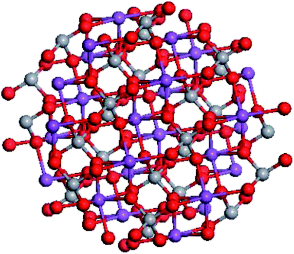 | ||
| Fig. 1 Structure of (BiVO4)26 nanocrystal sized 1.3 nm projected along the [010] crystallographic direction. | ||
Calculations of the electronic properties of nanocrystals require the use of two methodologies based on a semi-empirical approach and DFT theory to perform the simulations and also to ensure their stability. The semi-empirical approach uses the parameterised method referred to as PM6,50 which allows a pertinent evaluation of the physical features of clusters with large sizes and with the involvement of heavy atoms. Within such a framework, the numerical simulations were performed using the Gaussian09 quantum-chemical program package.51 All the calculations were made using restricted Hartree–Fock (RHF) regime with the SCF convergence criterion set at 10−5 kcal mol−1. The second approach was based on DFT calculations with Gaussian09 and DMol3 programs, i.e. Density functional for Molecules and 3-Dimensional periodic solids software as implemented in the Materials Studio package.51–54 The calculations were performed using the PBE48 and B3LYP55–58 functionals applying to atomic orbitals with the DND and CEP-4G basis sets. No symmetry rules were imposed during the electronic structure analysis. The SCF density convergence criterion was equal to 10−8 eV. In order to reduce the required computational time, all the core electrons were represented by effective core pseudopotentials.59,60 With regard to the size of the investigated clusters, the single point calculations were performed applying the RHF method.
Within such approaches, the electronic properties of three different clusters families were computed. The first one dealt with (BiVO4)n clusters possessing a monoclinic crystal structure without any reconstruction. The second family of clusters considered the same input structures as specified previously but their geometries were fully optimised according to the total energy minimisation. This means that the distances between the atoms change with taking into account the influence of surface limitation. The performed procedure simulates the amorphisation effect of the crystal structure. The geometry optimisation was performed in Cartesian coordinates of atoms with a C1 symmetry. The gradient convergence tolerance was equal to 10−6 Hartree/Bohr using the quadratic approximation (QA) method updating the Hessian matrix during the optimisation. The Hessian evaluation was performed to exclude those structures giving rise to negative modes. The third family of the investigated clusters included structures with partial reconstruction occurring on the cluster surface. In this case, the geometry optimisation procedure was performed applying the PCM solvent model, where the environment was modelled as BiVO4 nanoclusters with dielectric parameters measured at room temperature.61
To sum up, the present work deals with numerical modelling of the electronic properties of BiVO4 clusters with different configurations. On the one hand, these consist of clusters with frozen atomic positions, as also involved in the monoclinic phase, while on the other hand, reconstructed clusters possessing an amorphous structure and other partially reconstructed ones with the amorphisation gradually modified from the surface to the internal cluster core were also considered.
Results and discussion
Peculiarities of the bulk BiVO4 monoclinic structure
Usually quantum-chemical calculations of electronic properties of crystal materials are evaluated after achieving the geometry optimisation. In the present work, we propose two approaches to compute the electronic peculiarities of the BiVO4 crystal: first, by the usual methodology starting from geometry optimisation of the structure and then via calculation of its electronic properties, and second, by using the X-ray specified atomic positions with the defined lattice parameters involved in the monoclinic structure of BiVO4 without any lattice modification. The electronic properties were then evaluated. In this case, the quantum-chemical calculations were carried out for the geometry optimised structure and for the frozen crystal structure. The lattice parameters obtained from the geometry optimisation and the corresponding data from the X-ray studies are summarised in Table 1.| Parameters | Experimental structure (frozen atom positions) | Optimised structure |
|---|---|---|
| Bi–O bond length [Å] | 2.352 Å | 2.495 Å |
| 2.372 Å | 2.455 Å | |
| 2.518 Å | 2.437 Å | |
| V–O bond length [Å] | 1.762 Å | 1.740 Å |
| 1.688 Å | 1.744 Å | |
| Lattice parameters | a = 7.247 Å | a = 7. 330 Å |
| b = 11.697 Å | b = 11.649 Å | |
| c = 5.090 Å | c = 5.1932 Å | |
| γ = 134.226° | γ = 135.446° |
The geometry optimisation procedure revealed that the Bi–O bond lengths have a tendency to be symmetrical. The same situation is observed for V–O bonds. The possible reason for such isotropic bond lengths arrangement in the case of Bi–O connection is due to the strong correlation between the Bi 6s and the O 2p orbitals.34 The changes in the interatomic distances occurring during geometry optimisation influence the electronic properties of the structure. The energy dispersion curves of occupied and unoccupied states exhibit a similar behaviour for the optimised and frozen structures (see Fig. 2), but the energy gap was less by 0.24 eV for the optimised structure compared to the frozen structure. The results obtained for the optimised structure are consistent with the data published by Zhao et al.,32 where the band gap was evaluated as 2.17 eV by using the GGA/PBE potential. For the frozen structure of BiVO4, the band gap of 2.41 eV is consistent with the experimental reports.32,44 In both cases, the optimised and frozen structures possess an indirect band gap (see Fig. 2), which was confirmed by the experimental results presented in the work of Venkatesan et al.62 and Cooper et al.63
 | ||
| Fig. 2 The band structures calculated for the frozen BiVO4 crystal structure. | ||
The partial density of states (DOS) for the monoclinic BiVO4 crystal structure was also computed and used to compare the electronic features of the frozen (not optimised) structure with the optimised bulk structure. The partial DOS calculated for the optimised monoclinic BiVO4 phase is presented in Fig. 3. This underlines that the top of the valence band was built by hybridisation of the O 2p and V 3p states. The minimum of the conduction band was dominated by V 3d states with small contributions from Bi 6p and O 2p orbitals, as was also seen for the frozen BiVO4 structure (see Fig. 4). Contrary to the DOS of the optimised structure, the main contributions to the valence band states of the frozen BiVO4 crystal structure were from O 2p orbitals slightly hybridised with Bi 6s states. Usually, the valence band in metal oxides is derived from O 2p orbitals and the conduction band is built by metal s or d orbitals. However, in monoclinic BiVO4, the valence band contains hybrid Bi 6s and O 2p orbitals, which causes an upward dispersion of the electronic structure at the zone boundary.37 This indicates that the frozen structure allows sound analysis of the electronic features of the BiVO4 crystal. The distortions of Bi–O and V–O bond lengths during geometry optimisation enhance the impact of the Bi 6s states and this contributes to more dispersion in the valence band. These result are in agreement with the data measured by using the XPS64 method. The obtained results suggest that, from a computational point of view, both structures – optimised and frozen – lead to reasonable results. The obtained data make it possible to infer that modelled nano-sized clusters should be constructed with protection of the crystal internal structure and with optimised external atomic shells, according to the surface effects and environmental interactions.
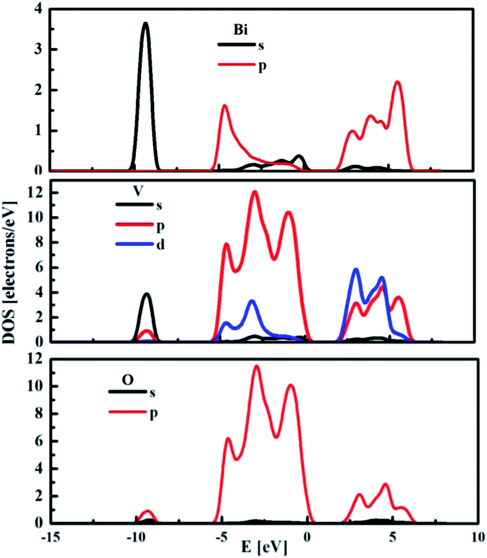 | ||
| Fig. 3 The partial density of states for monoclinic BiVO4 optimised structure. | ||
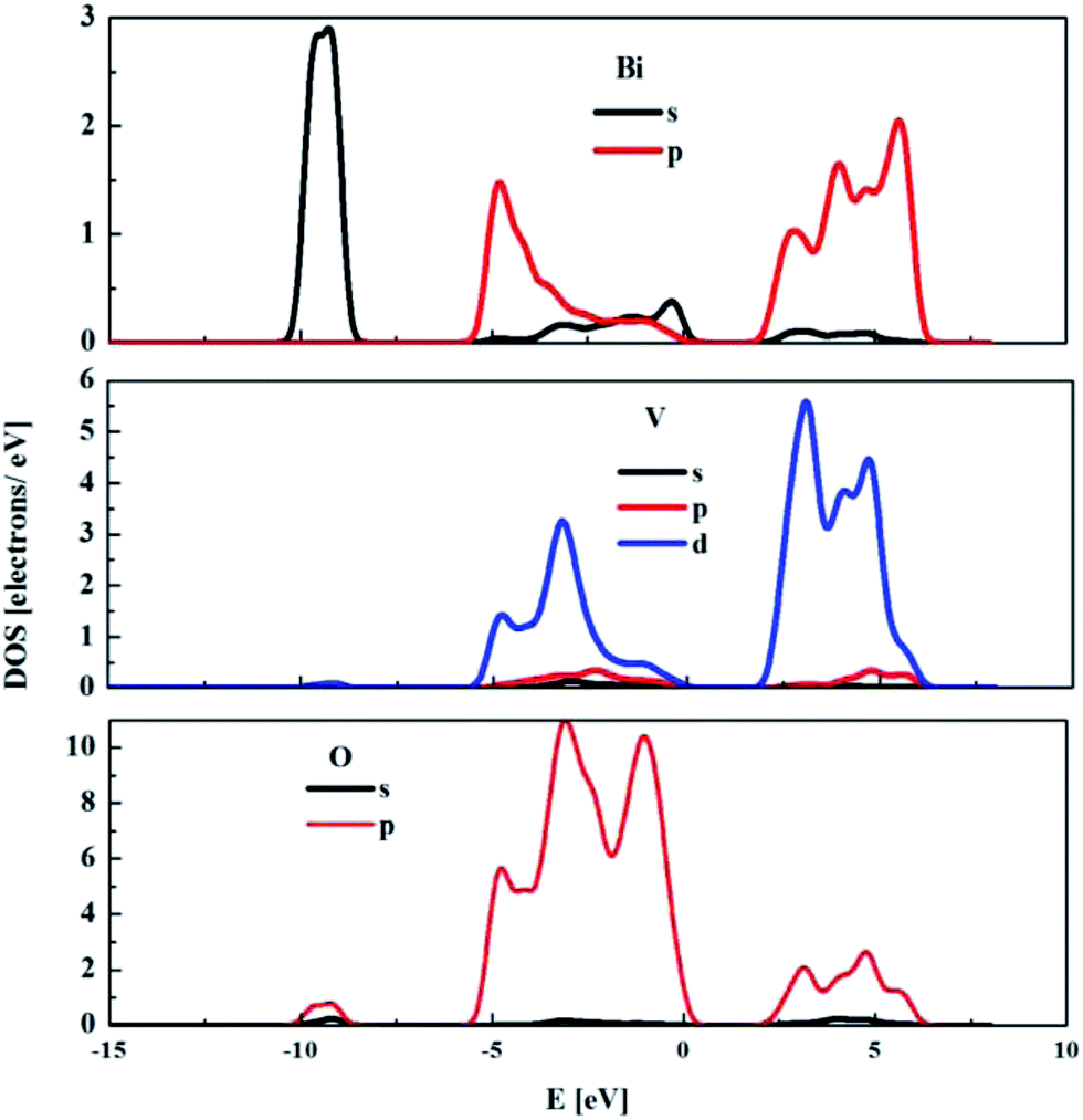 | ||
| Fig. 4 The partial density of states for monoclinic BiVO4 frozen (no optimised) structure. | ||
The simulated energy band structure for the frozen bulk BiVO4 structure leads to the effective masses of the charge carriers. The energy dispersion curves of VBM and CBM are symmetrical, respectively around the (−0.5, 0, 0) and (0, −0.5, 0.5) points of the Brillouin zone (see Fig. 2). In this case the calculated electrons and holes effective masses were equal to 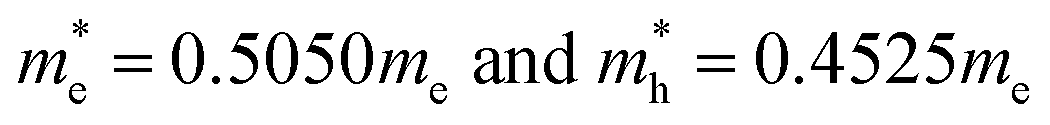 , respectively. These evaluations are in a good agreement with the work of Huang et al.65 and Zhao et al.32,42 One might expect that the mobility of charges in the nanoparticle core would be similar to that involved in the crystalline bulk structure. In semiconducting oxides, the valence bands formed by localised oxygen p orbitals lead to an increase in the effective mass of the holes. The VB of BiVO4 is composed of O 2p and Bi 6s electrons, with a strong correlation between them ensuring a decrease in the effective mass of the holes and an increase in their mobility. Such a light mass of holes is expected to facilitate efficient photoinduced charge separation and mobility, suggesting a possibility of high quantum efficiency in photocatalysis.
Electronic structure analysis for BiVO4 nanoclusters
The general advantage of nanostructured systems is related to their high surface areas, which increase the efficiency of photocatalytic reactions.66,67 The present work aimed to carry out exhaustive numerical evaluations of the electronic and vibration properties of nano-sized (BiVO4)n particles, built as described in the previous section. The number n of the structural units was changed from n = 1 up to n = 56, leading to a cluster diameter of up to 2.0 nm. To compute the physical properties of nanocrystals, the cluster approach was applied treating the inorganic nanostructure as molecules without any surface saturation. According to our previous work on other classes of nanocrystalline oxide systems, dangling bonds were not specially treated.30,68 The physical properties of the clusters were calculated for frozen clusters possessing a fixed position of atoms as well as for relaxed ones according to the geometry optimisation procedure described in the previous section. The electronic properties of spherically shaped clusters were computed by using DFT/PBE and DFT/B3LYP methodologies implemented in the DMOL3 program. Although the DFT functionals correctly evaluated the changes in the energy band gap versus the cluster size, thus exhibiting the size inducing quantum confinement effect, the obtained results are underestimated compared to the experimental data. Alternatively, the semi-empirical PM6 parameterised method was used to calculate the electronic properties of isolated (BiVO4)n clusters. The calculated energy difference between the highest occupied molecular orbital (HOMO) and lowest unoccupied molecular orbital (LUMO) was defined as the ΔEHOMO–LUMO energy gap splitting, as shown in Fig. 5 (top panel). The figure presents the evaluation of the ΔEHOMO–LUMO calculated for the frozen and optimised structures versus their size. In both cases, this means that for crystalline and amorphous nanoparticles, one may see that, with increasing the size of nanoclusters, their energy gap decreases in agreement with the size inducing quantum confinement effect. The related changes of ΔEHOMO–LUMO calculated for crystalline and amorphous nanoparticles are consistent with the data presented by Chattopadhyay et al.23,24 In these reports, the authors showed experimentally that BiVO4 nanocrystals possess an indirect band gap in the range of 3.51–3.67 eV or 2.75–2.82 eV, depending on the sample preparation and the particle size. The reported results for crystalline clusters are lower than those for amorphous structures. These results suggest that the measured clusters must have an amorphous fraction at their surface and a better crystalline order in their core part. | ||
| Fig. 5 The energy gap splitting (ΔEHOMO–LUMO) versus cluster size calculated by the PM6 method for (BiVO4)n clusters. Top panel reports the data obtained for frozen and optimised structures. Bottom panel shows the results obtained for partially optimised structures. | ||
The bottom panel of Fig. 5 shows ΔEHOMO–LUMO calculated by the PM6 method for partially optimised clusters. The surfaces of these clusters were reconstructed according to the environmental interaction acting on BiVO4 nanoparticles. The cluster optimisation was performed shell by shell starting from the surface and progressing to the core of the nanoparticle, taking the RMS difference for two successive optimisations as less than 1%. The obtained results, evaluating the ΔEHOMO–LUMO, can be divided into two parts, as marked by rectangles and triangles in the bottom panel of Fig. 5. The first class of data, represented by rectangles, traduces qualitatively the expected size inducing quantum confinement effect, as illustrated for BiVO4 optimised nanoparticles (see Fig. 5, top panel). The second set of data, represented by triangles, reflects the behaviour of the frozen BiVO4 structure. The computed data, represented by triangles, fluctuate with increasing the cluster size, but they have a tendency to be aligned to an asymptotic value close to 2.4 eV. The same value of energy gap was obtained for the bulk frozen crystal structure of BiVO4 as well as for non-optimised nanocrystals with a size greater than 1.0 nm (nanocrystals with n > 10). The obtained results are in good agreement with the data presented by Sun et al.20 Calculations performed for partially reconstructed clusters show that for nanoparticles smaller than 1.1 nm (n < 20), the physical peculiarities are generally dominated by surface effects. For larger particles (sizes above 1.8 nm, n > 40), the surface influence is less pronounced compared to core atoms keeping the same coordinates as involved in a monoclinic crystal structure.
The electronic properties were exhaustively studied for the partially reconstructed cluster with the size of 1.2 nm (n = 18). The obtained results confirm that the top of the HOMO orbital is built by the O 2p oxygen states and the LUMO is created by V 3d orbitals. The data reported in Fig. 6 underline that the HOMO and LUMO orbitals are located in the reconstructed, surface part of the cluster. Compared to the bulk material where the VBM was created by O 2p orbitals hybridised by V 3p and Bi 6s for the optimised and frozen structure, respectively, one could conclude that the size reduction of the investigated cluster does not drastically change its electronic properties.
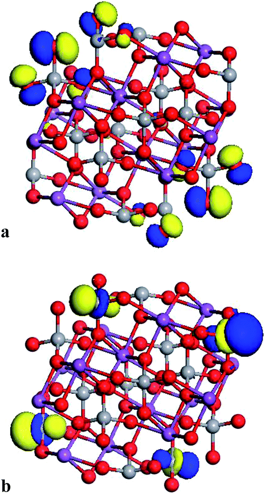 | ||
| Fig. 6 Visualisation of the HOMO (a) and LUMO (b) orbitals computed by PM6 semi-empirical method for the partially reconstructed cluster with size 1.2 nm. | ||
The partial DOS computed for the partially reconstructed (BiVO4)18 cluster indicates that the highest occupied energy levels are associated mainly with the O 2p states hybridised with Bi 6p (Fig. 7). Similar properties were demonstrated for the bulk monoclinic BiVO4 with frozen atomic coordinates. The main difference between the DOS of the bulk system and the nanocluster seems to be related to the contribution from Bi 6s and Bi 6p states, respectively. Moreover, it is worth noting that for nanocrystalline (BiVO4)18, a strong correlation is involved between Bi and O orbitals. This confirms that the electronic properties of the simulated cluster are mainly driven by the core atoms. The unoccupied orbitals with the lowest energy are composed mainly by V 3d states, with small contributions from Bi 6p and O 2p states, as was also observed for the bulk system.
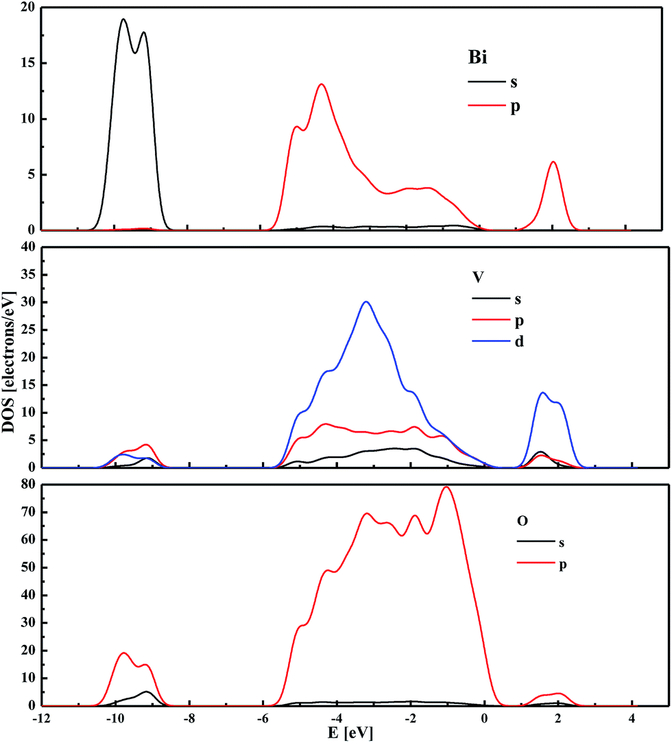 | ||
| Fig. 7 The partial density of states calculated by the PM6 semi-empirical method for the partially reconstructed cluster sized 1.2 nm. | ||
The optical properties of the partially reconstructed cluster (BiVO4)18 and those of the frozen monoclinic BiVO4 single crystal were also calculated. The obtained UV-vis absorption spectra related to both configurations are shown in Fig. 8 (top panel). The absorption edge calculated for the nano-sized cluster was shifted to higher energy compared to that of the bulk crystal. Such a difference is characteristic of the size inducing quantum confinement effect and is in agreement with the work of Karunakaran et al.22 Moreover, for the bulk infinite structure, the optical spectrum is more extended, with two main features reflecting the indirect band gap system. The UV absorption observed in monoclinic BiVO4 is associated with a band transition from O 2p to V 3d, whereas visible light absorption is due to the transition from a valence band formed by Bi 6s or a hybrid orbital of Bi 6s and O 2p to a conduction band of V 3d. This is in agreement with the data presented in the work of Ng et al.69 The relevance of the performed calculations was confirmed by comparing with the experimental studies. The optical properties were investigated by using the Ocean Optics UV-Vis spectrometer in a wavelength range from 100 nm to 1000 nm. Indeed, the calculated UV-vis absorption spectrum for the partially reconstructed (BiVO4)18 structure presented similar features with the experimental spectrum obtained on mesoporous BiVO4 (see Fig. 8, bottom panel). As it will be reported elsewhere, the experiments were carried out on mesoporous thin films synthesised by the sol–gel method with a suitable surfactant to ensure nanostructured samples. The energy band gap of BiVO4 mesoporous thin film could be estimated from plotting the square of the Kubelka–Munk functions F(R) versus photon energy, as shown in Fig. 8. The tangential line, which is extrapolated to [F(R)]2 = 0, indicates a band gap of 2.55 eV. The absorption cut-off wavelength was about 490 nm for a mesoporous thin film and as calculated for a partially reconstructed (BiVO4)18 cluster, suggesting the potential photoactivity of such a material under visible radiation. Additionally, the surface of the partially reconstructed nanoparticles was modified according to the environmental effect of the interacting bismuth vanadate. In this case, the implemented cluster model of partially modified structures is a good model for a mesoporous material to predict its electronic properties as crucial for photocatalytic applications.
 | ||
| Fig. 8 (Top panel) Theoretical UV-vis absorption spectra calculated for bulk (solid line) and nano-sized (dashed line) BiVO4 structures by using the DFT/PBE and semi-empirical PM6 parameterised methods, respectively. (Bottom panel) Experimental optical response of mesoporous thin film of BiVO4 represented by Kubelka–Munk function, giving an absorption edge at 2.55 eV. | ||
To sum up, the experimental optical features obtained on a mesoporous material are consistent with the theoretical calculations carried out for partially reconstructed nanostructures. This close correlation makes us confident in the developed numerical approach to analyse the electronic and optical effects of this class of semiconducting oxides. The quantum confinement effect was well demonstrated theoretically on the optical spectrum of a nano-sized cluster. The photoinduced charge transfer mechanism under visible light radiation is of primary importance for the photocatalytic responses of this class of materials. In the same context, nanostructured systems composed of nanoparticles possess high specific surfaces, which play a crucial role in heterogeneous photocatalysis. This was also confirmed by the fact that the active HOMO and LUMO orbitals were located at the nanoparticle surface. However, as was shown from our calculations, the spectral range of absorbed sunlight observed for nanoparticles was shifted to higher energies, which limits the absorption quantum efficiency. Thus, a balance must be achieved between the size reduction and the induced widening of the band gap. This task is a hot topic in major photoinduced phenomena since the modulation of the electronic structure and density of states may be ensured by the size and shape design.
Vibrational properties of BiVO4 nanoclusters
The vibrational properties were analysed for clusters with frozen and optimised (BiVO4)n atomic coordinates. As discussed above, the frozen clusters possess the same atomic arrangement involved in monoclinic bismuth vanadate. The optimised structures have a tendency to stabilise in amorphous configurations according to the requirement of the total energy minimum. The IR absorption spectra calculated by PM6 methodology for both cluster families are presented in Fig. 9. Experimental reports performed by Zhang et al.70 showed that BiVO4 nanoparticles are characterised by a broad and strong IR band near 728 cm−1 with shoulders at 892, 822, 684 and 632 cm−1. From our computational work, the calculated spectra for the frozen structure of nanoparticles show also a broad band around 800 cm−1, which develops for large-sized clusters. This result suggests that there is a significant influence on the vibrational fingerprints from core atoms of the nanoparticles, particularly when the cluster size increases. For small clusters, more influence on the vibrational properties occurs from surface atoms. This is illustrated in the case of clusters with small sizes (Fig. 8, bottom panel), where the IR signature is quite different for the optimised and frozen configurations. This contrasts with large-sized clusters, such as (BiVO4)44, where the same shape of the IR spectra was qualitatively obtained irrespective of the atomic arrangement being optimised or frozen. The main reason for such a behaviour lies in the optimisation procedure inducing reconstruction and relaxation at the outermost cluster surfaces while preserving the core atoms. As the small clusters are highly sensitive to surface atoms, in contrast to large-sized clusters, drastic changes occur on their IR spectra, as demonstrated from the performed calculations.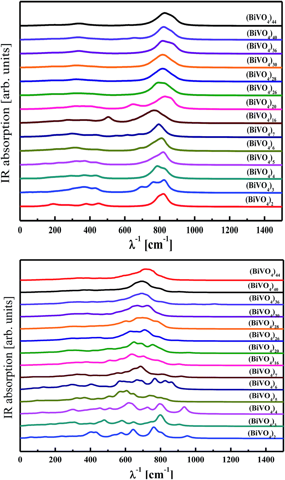 | ||
| Fig. 9 IR spectra calculated by PM6 methodology for frozen (top panel) and optimised (bottom panel) (BiVO4)n clusters of different sizes. | ||
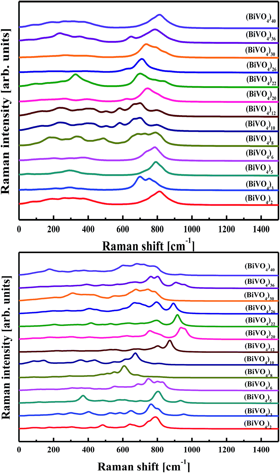
Taking into account the effect of electron–phonon interaction, evaluation of the Raman spectra related to the selected clusters was performed utilising the PM6 approach. The Raman spectra were calculated using a standard procedure implemented in the Gaussian program package. The calculations were performed for frozen and geometry optimised (BiVO4)n clusters; the latter being characterised by an amorphous network. The calculated Raman spectra, without any applied scissor recalculations, are presented in Fig. 10. Similar conclusions can be drawn between the calculated IR and Raman spectra. In particular, the main contribution occurs from core atoms of the clusters. For small clusters, where the ratio of the surface atoms to the internal ones is high, the main band located at 800 cm−1 is shifted and the spectrum part in the low wavenumber range is less detailed. The Raman spectrum performed for nano-sized BiVO4 is dominated by an intense Raman band at 827 cm−1, assigned to vs(V–O), and with a weak shoulder at about 709 cm−1, assigned to vas(V–O).70 In the calculated Raman spectrum for (BiVO4)40, one may notice the non-symmetric band at a position of 800 cm−1 with the same shoulder depicted in the low wavenumber part.
 | ||
| Fig. 10 Raman spectra calculated by PM6 methodology for frozen (top panel) and optimised (bottom panel) (BiVO4)n clusters with different sizes. | ||
In Fig. 11, a tentative comparison is made between the Raman spectra calculated by PM6 methodology for frozen and optimised (BiVO4)18 clusters and the experimental spectrum performed with the laser radiation at 568 nm on the mesoporous thin film of BiVO4. The experimental spectrum is characterised by a main peak at a position of around 800 cm−1, as seen for the frozen structure of (BiVO4)18 (band depicted as A). This contrasts with the amorphous structure, where such a band is absent due to the V–O distances being relaxed by the stabilisation criterion based on the total energy minimisation procedure. Only a broad feature is seen around 900 cm−1. It is worth noting a similar behaviour reported in our previous work devoted to the vibrational properties of NiTiO3 nanoparticles.30
 | ||
| Fig. 11 Raman spectra calculated by PM6 methodology for frozen (black solid line) and optimised (black dashed line) (BiVO4)n clusters and the experimental one performed with laser radiation 568 nm (red line). | ||
The experimental Raman spectrum reported for BiVO4 nanoparticles is characterised also by δs(VO43−) and δas(VO43−) modes at 366 and 324 cm−1, respectively.70 In the case of a mesoporous thin film structure, both Raman bands are resolved with high intensity, but the second peak is more pronounced (Fig. 11, band B′). From the computational results on the frozen (BiVO4)18 cluster, a similar behaviour is observed (Fig. 11, band B). The small discrepancy in the band positions may be explained by the fact that anharmonic vibration terms were not considered in the calculation model. The bands labelled as C are seen for the geometry optimised (BiVO4)40 cluster and occur probably from the same vibrational features as those leading to the bands at 366 and 324 cm−1. However, the V–O bond length changes modify the Raman band positions and amorphisation of the cluster by geometry optimisation creates a wavenumber distribution that broadens the bands, leading to features of the vibrational density of states.71
Conclusions
Quantum theory approaches based on DFT and semi-empirical models were applied on semiconducting oxides, such as BiVO4, dedicated to photocatalytic applications. A bulk infinite crystalline structure with a monoclinic scheelite polytype was built and the corresponding electronic properties were determined by using the CASTEP program. Two approaches were developed to compute the electronic properties of the BiVO4 crystal: one involving clusters submitted to a geometry optimisation procedure, and a second one possessing frozen positions of the atoms. The performed calculations demonstrated the validity of the calculation for the frozen structure, which was necessary to build a cluster model of (BiVO4)n with n = 1 ÷ 44. The electronic and vibration properties of the (BiVO4)n nanostructures were calculated versus the cluster size.The simulations of the structural and electronic properties of the nanostructures were performed by using the semi-empirical model known as PM6 and the second based on the DFT method. The used (BiVO4)n clusters were chosen with sizes up to 2 nm consisting of clusters with frozen atomic positions, optimised ones or ones with partially reconstructed structures according to the environmental interactions. The DFT implemented in DMol3 software with the B3LYP and PBE functionals was used for the evaluation of the electronic features. However, the obtained results and particularly the ΔEHOMO–LUMO energy did not reflect the experimental values. In contrast to the DFT method, relevant evaluations of the HOMO–LUMO energies were obtained by using the semi-empirical PM6 model. Furthermore, the calculations showed that the structural electronic and vibrational properties of the nano-sized BiVO4 clusters depend more on the importance of the surface atoms compared to the core ones. In particular, small clusters show a reconstruction leading to an amorphous structure, while larger clusters favour a crystalline order for their core atoms. The computational work demonstrated that the physical features correlate drastically with (BiVO4)n clusters with small sizes due to the dominant contributions of the surface atoms. Among the consequence of the performed calculations, a consistent insight can be drawn on the potential application of the considered semiconducting oxides. This is illustrated by the photocatalytic activity, which requires a compromise between the nanostructure sizes (specific surfaces) and the ability to harvest a large spectral range from sun radiation (small band gap). This last criterion needs nanocrystals with core atoms keeping the same coordinates as involved in the monoclinic scheelite structure.
Acknowledgements
M. Makowska-Janusik is thankful to COST Action MP1202 action for the financial assistance. Calculations have been carried out in Wroclaw Center for Networking and Supercomputing ‘http://www.wcss.wroc.pl’ (Grant no. 171). The MATERIALS STUDIO package was used under POLAND COUNTRY-WIDE LICENSE. K. Ordon has benefited in 2016 of Scholarship “Excellence Eiffel grant” from French Ministry of foreigner affairs. The authors would like to thank Dr Sandrine Coste for her contribution on experimental synthesis of BiVO4.Notes and references
- K. Hashimoto, H. Irie and A. Fujishma, Jpn. J. Appl. Phys., 2005, 44, 8269 CrossRef CAS.
- X. Kong, C. Liu, W. Dong, X. Zhang, C. Tao, L. Shen, J. Zhou, Y. Fei and S. Ruana, Appl. Phys. Lett., 2009, 94, 123502 CrossRef.
- H. Liu, R. Nakamura and Y. Nakato, J. Electrochem. Soc., 2005, 152, 856 CrossRef.
- J. B. Liu, H. Wang, S. Wang and H. Yan, Mater. Sci. Eng., B, 2003, 104, 36 CrossRef.
- A. Kudo, K. Omori and H. Kato, J. Am. Chem. Soc., 1999, 121, 11459 CrossRef CAS.
- A. Kudo, K. Ueda, H. Kato and I. Mikami, Catal. Lett., 1998, 53, 229 CrossRef CAS.
- S. Kohtani, M. Koshiko, A. Kudo, K. Tokumura, Y. Ishigaki, A. Toriba, K. Hayakawa and R. Nakagaki, Appl. Catal., B, 2003, 46, 573 CrossRef CAS.
- S. Tokunaga, H. Kato and A. Kudo, Chem. Mater., 2001, 13, 4624 CrossRef CAS.
- X. Zhang, Z. Ai, F. Jia, L. Zhang, X. Fan and Z. Zou, Mater. Chem. Phys., 2007, 103, 162 CrossRef CAS.
- S. Tokunaga, H. Kato and A. Kudo, Chem. Mater., 2001, 13, 4624 CrossRef CAS.
- M. Wang, Q. Liu, Y. Che, L. Zhang and D. Zhang, J. Alloys Compd., 2013, 548, 70 CrossRef CAS.
- H. Xu, H. Limailto, C. Wu, J. Chu, Y. Yan and H. Shu, Mater. Sci. Eng., B, 2008, 147, 52–56 CrossRef CAS.
- S. P. Berglund, A. J. E. Rettie, S. Hoang and C. B. Mullins, Phys. Chem. Chem. Phys., 2012, 14, 7065 RSC.
- L. Ren, L. Jin, J.-B. Wang, F. Yang, M.-Q. Qiu and Y. Yu, Nanotechnology, 2009, 20, 115603 CrossRef PubMed.
- W. Wang, X. Huang, S. Wu, Y. Zhou, L. Wang, H. Shi, Y. Liang and B. Zou, Appl. Catal., B, 2014, 74, 294 Search PubMed.
- M.-L. Guan, D.-K. Ma, S.-W. Hu, Y.-J. Chen and S.-M. Huang, Inorg. Chem., 2011, 50, 800 CrossRef CAS PubMed.
- S. J. Hong, S. Lee, J. S. Jang and J. S. Lee, Energy Environ. Sci., 2011, 4, 1781 CAS.
- Y. Yang, Y. Liu, B. Huang, R. Zhang, Y. Dai, X. Qin and X. Zhang, RSC Adv., 2014, 4, 20058 RSC.
- Y. Geng, P. Zhang and S. Kuang, RSC Adv., 2014, 4, 46054 RSC.
- S. Donga, J. Feng, Y. Li, L. Hu, M. Liu, Y. Wang, Y. Pi and J. Sun, Appl. Catal., B, 2014, 152–153, 413 CrossRef.
- Y. Lu, H. Shang, F. Shi, C. Chao, X. Zhang and B. Zhang, J. Phys. Chem. Solids, 2015, 85, 44 CrossRef CAS.
- C. Karunakaran, S. Kalaivani, P. Vinayagamoorthy and S. Dash, Mater. Sci. Semicond. Process., 2014, 21, 122–131 CrossRef CAS.
- S. Sarkar and K. K. Chattopadhyay, Phys. E, 2012, 44, 1742 CrossRef CAS.
- S. Sarkar, N. S. Das and K. K. Chattopadhyay, Solid State Sci., 2014, 33, 58 CrossRef CAS.
- A. R. Limt, S. H. Choh and M. S. Jang, J. Phys.: Condens. Matter, 1995, 7, 7309 CrossRef.
- L. Zhang, D. R. Chen and X. L. Jiao, J. Phys. Chem. B, 2006, 110, 2668 CrossRef CAS PubMed.
- L. Zhou, W. Z. Wang, S. W. Liu, L. S. Zhang, H. L. Xu and W. Zhu, J. Mol. Catal. A: Chem., 2006, 252, 120 CrossRef CAS.
- J. G. Yu and A. Kudo, Adv. Funct. Mater., 2006, 16, 2163 CrossRef CAS.
- A. Galembeck and O. L. Alves, Thin Solid Films, 2000, 365, 90 CrossRef CAS.
- M. A. Ruiz Preciado, A. Kassiba, A. Morales-Acevedo and M. Makowska-Janusik, RSC Adv., 2015, 5, 17396 RSC.
- W. J. Yin, S. H. Wei, M. M. Al-Jassim, J. Turner and Y. Yan, Phys. Rev. B: Condens. Matter Mater. Phys., 2011, 83, 155102 CrossRef.
- Z. Zhao, Z. Li and Z. Zou, Phys. Chem. Chem. Phys., 2011, 13, 4746 RSC.
- J. K. Cooper, S. Gul, F. M. Toma, L. Chen, P.-A. Glans, J. Guo, J. W. Ager, J. Yano and I. D. Sharp, Chem. Mater., 2014, 26, 5365 CrossRef CAS.
- J. Ma and L.-W. Wang, Appl. Phys. Lett., 2014, 105, 172102 CrossRef.
- M. Oshikiri, M. Boero, J. Ye, Z. Zou and G. Kido, J. Chem. Phys., 2002, 117, 7313 CrossRef CAS.
- K. Sayama, A. Nomura, T. Arai, T. Sugita, R. Abe, M. Yanagida, T. Oi, Y. Iwasaki, Y. Abe and H. Sugihara, J. Phys. Chem. B, 2006, 110, 11352 CrossRef CAS PubMed.
- A. Walsh, Y. Yan, M. N. Huda, M. M. Al-Jassim and S. H. Wei, Chem. Mater., 2009, 21, 547 CrossRef CAS.
- M. W. Stoltzfus, P. M. Woodward, R. Seshadri, J.-H. Klepeis and B. Bursten, Inorg. Chem., 2007, 46, 3839 CrossRef CAS PubMed.
- M. Oshikiri and M. Boero, J. Phys. Chem. B, 2006, 110, 9188 CrossRef CAS PubMed.
- M. Oshikiri, M. Boero, A. Matsushita and J. Ye, J. Electroceram., 2009, 22, 114 CrossRef CAS.
- K. E. Kweon and G. S. Hwang, Appl. Phys. Lett., 2013, 103, 131603 CrossRef.
- Z. Zhao, W. Luo, Z. Li and Z. Zou, Phys. Lett. A, 2010, 374, 4919 CrossRef CAS.
- J. Yang, D. Wang, X. Zhou and C. Li, Chem.–Eur. J., 2013, 19, 1320 CrossRef CAS PubMed.
- K. Ding, B. Chen, Y. Li, Y. Zhangab and Z. Chenc, J. Mater. Chem. A, 2014, 2, 8294 CAS.
- A. W. Sleight, H. Y. Chen, A. Ferretti and D. E. Cox, Mater. Res. Bull., 1979, 14, 1571 CrossRef CAS.
- Y. Park, K. J. McDonald and Q.-S. Choi, Chem. Soc. Rev., 2013, 42, 2321 RSC.
- J.-C. Liu, J.-P. Chen and D.-Y. Li, Acta Phys. Sin., 1983, 32, 1053 CAS.
- J. P. Perdew, K. Burke and M. Ernzerhof, Phys. Rev. Lett., 1996, 77, 3865 CrossRef CAS PubMed.
- B. G. Pfrommer, M. Côté, S. G. Louie and M. L. Cohen, J. Comput. Phys., 1997, 131, 233 CrossRef CAS.
- J. J. P. Stewart, J. Mol. Model., 2007, 13, 1173 CrossRef CAS PubMed.
- M. J. Frisch, G. W. Trucks, H. B. Schlegel, G. E. Scuseria, M. A. Robb, J. R. Cheeseman, G. Scalmani, V. Barone, B. Mennucci, G. A. Petersson, H. Nakatsuji, M. Caricato, X. Li, H. P. Hratchian, A. F. Izmaylov, J. Bloino, G. Zheng, J. L. Sonnenberg, M. Hada, M. Ehara, K. Toyota, R. Fukuda, J. Hasegawa, M. Ishida, T. Nakajima, Y. Honda, O. Kitao, H. Nakai, T. Vreven, J. A. Montgomery Jr, J. E. Peralta, F. Ogliaro, M. Bearpark, J. J. Heyd, E. Brothers, K. N. Kudin, V. N. Staroverov, T. Keith, R. Kobayashi, J. Normand, K. Raghavachari, A. Rendell, J. C. Burant, S. S. Iyengar, J. Tomasi, M. Cossi, N. Rega, J. M. Millam, M. Klene, J. E. Knox, J. B. Cross, V. Bakken, C. Adamo, J. Jaramillo, R. Gomperts, R. E. Stratmann, O. Yazyev, A. J. Austin, R. Cammi, C. Pomelli, J. W. Ochterski, R. L. Martin, K. Morokuma, V. G. Zakrzewski, G. A. Voth, P. Salvador, J. J. Dannenberg, S. Dapprich, A. D. Daniels, O. Farkas, J. B. Foresman, J. V. Ortiz, J. Cioslowski and D. J. Fox, Gaussian 09, Revision E.01, Gaussian, Inc., Wallingford CT, 2013 Search PubMed.
- M. S. Modelling, Release 3.0.1, Accelrys Inc., San Diego, 2004 Search PubMed.
- B. Delley, J. Chem. Phys., 1990, 92, 508 CrossRef CAS.
- B. Delley, J. Chem. Phys., 2000, 113, 7756 CrossRef CAS.
- A. D. Becke, J. Chem. Phys., 1993, 98, 5648 CrossRef CAS.
- C. Lee, W. Yang and R. G. Parr, Phys. Rev. B: Condens. Matter Mater. Phys., 1988, 37, 785 CrossRef CAS.
- S. H. Vosko, L. Wilk and M. Nusair, Can. J. Phys., 1980, 58, 1200 CrossRef CAS.
- P. J. Stephens, F. J. Devlin, C. F. Chabalowski and M. J. Frisch, J. Phys. Chem., 1994, 98, 11623 CrossRef CAS.
- M. Dolg, U. Wedig, H. Stoll and H. Preuss, J. Chem. Phys., 1987, 86, 866 CrossRef CAS.
- A. Bergner, M. Dolg, W. Kuechle, H. Stoll and H. Preuss, Mol. Phys., 1993, 80, 1431 CrossRef CAS.
- K. V. R. Prasad and K. B. R. Varma, Mater. Chem. Phys., 1994, 38, 406 CrossRef CAS.
- R. Venkatesan, S. Velumani and A. Kassiba, Mater. Chem. Phys., 2012, 135, 842 CrossRef CAS.
- J. K. Cooper, S. Gul, F. M. Toma, L. Chen, J. W. Ager, J. Yano and I. D. Sharp, J. Phys. Chem. C, 2015, 119, 2969 CAS.
- D. J. Payne, M. D. M. Robinson, R. G. Egdell, A. Walsh, J. McNulty, K. E. Smith and L. F. J. Piper, Appl. Phys. Lett., 2011, 98, 212110 CrossRef.
- Z.-F. Huang, L. Pan, J.-J. Zou, X. Zhang and L. Wang, Nanoscale, 2014, 6, 14044 RSC.
- Y. J. Kim, B. Gao, S. Y. Han, M. H. Jung, A. K. Chakraborty, T. Ko, C. Lee and W. I. Lee, J. Phys. Chem. C, 2009, 113, 19179 CAS.
- K. Sivula, R. Zboril, F. Le Formal, R. Robert, A. Weidenkaff, J. Tucek, J. Frydrych and M. Grätzel, J. Am. Chem. Soc., 2010, 132, 7436 CrossRef CAS PubMed.
- M. Makowska-Janusik, O. Gladii, A. Kassiba, J. Boucle and N. Herlin-Boime, J. Phys. Chem. C, 2014, 118, 6009 CAS.
- Y. H. Ng, A. Iwase, A. Kudo and R. Amal, J. Mater. Sci. Lett., 2010, 1, 2607 CAS.
- A. Zhang and J. Zhang, Mater. Sci.-Pol., 2009, 27, 1015 CAS.
- M. Makowska-Janusik, A. Kassiba, J. Bouclé, J. F. Bardeau, S. Kodjikian and A. Désert, J. Phys.: Condens. Matter, 2005, 17, 5101 CrossRef CAS.
| This journal is © The Royal Society of Chemistry 2016 |