MoO3@Ni nanowire array hierarchical anode for high capacity and superior longevity all-metal-oxide asymmetric supercapacitors

Chao Xua, Jie Liaoa, Ruozheng Wanga, Peichao Zoua, Ronghe Wanga, Feiyu Kangab and Cheng Yang*a
aDivision of Energy and Environment, Graduate School at Shenzhen, Tsinghua University, Shenzhen 518055, P. R. China. E-mail: yang.cheng@sz.tsinghua.edu.cn
bState Key Laboratory of New Ceramics and Fine Processing, Department of Materials Science and Engineering, Tsinghua University, Beijing 100084, China

Received 15th August 2016 , Accepted 31st October 2016

First published on 4th November 2016


Abstract

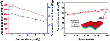
In this communication, a general technology for improving the electrochemical performances of metal oxide based electrode materials has been demonstrated via in situ growth of the electrode materials on Ni nanowire array (NNA) current collector films, which can attain a loading level up to ∼25 mg cm−2. The NNA@MoO3 electrode delivered a high areal capacity ∼477 mF cm−2 and superior longevity (∼5% capacitance loss after 20[thin space (1/6-em)]000 cycles). Moreover, crystalline VO2 was electro-deposited on NNA as the cathode, which was assembled with the NNA@MoO3 anode into an all-metal oxide-based asymmetric supercapacitor (AAS). The AAS can deliver an open circuit voltage of 1.6 V in an aqueous electrolyte and a high energy density (2.19 mW h cm−3) at the power density of 8.2 mW cm−3. This work provides an example of a flexible AAS device featuring a high areal capacity (307 mF cm−2) and excellent cyclability (116% retention after 20[thin space (1/6-em)]000 cycles) simultaneously purely involved with metal oxide electrodes.


Introduction

There is a growing demand for portable, miniaturized, low cost and high performance electronic devices for versatile applications such as wearable electronics, e-skin, and e-paper.1–3 For example, electrochemical energy storage units such as lithium ion batteries and supercapacitors featuring small sizes, high powers and long life spans have become more important than ever.4–6 Specifically, supercapacitors are a critical component due to their fast dynamic responses, superior cyclability, and integrated advantages over conventional capacitors (limited energy) and lithium ion batteries (limited power).7 Recently, all-metal-oxide based asymmetric supercapacitors (AASs) have attracted much attention by researchers due to the following reasons: (1) the open circuit voltage of the supercapacitor can be increased by choosing different electrode materials working in different potential ranges, (2) transition metal oxides typically show a high theoretical capacitance (usually >1000 F g−1), (3) there are several available metal oxide species showing superior performance characteristics, which are abundant in the earth and cheap, and sometimes are safer and more stable as compared with metal nitrides, metal carbides and metal sulfides. All of these features render them a promising candidate for future high-performance electrochemical energy storage applications. Therefore, a few transition metal oxides (such as MoO3,8 VO2,9 Fe2O3 (ref. 10) and MnO2 (ref. 11) etc.) have been intensively investigated for potential supercapacitor electrode applications. However, there are evident drawbacks for the metal-oxide-based electrode materials such as poor cyclability, which has been significantly hindering their technological development and commercial transfer. Therefore, scientists have conducted intensive studies for enhancing the electrochemical performance of the metal oxide-based supercapacitor electrodes. For example, nanostructured active materials have been explored for the purpose of increasing the surface area for better electrode/electrolyte contact and a short ion-diffusion length to accelerate the redox reactions at a high rate, including assembled nanoparticles, nanosheets and nanowires.12–14 Moreover, other approaches such as elemental doping and compositing conductive materials have been proven effective solutions to enhance the overall electrochemical performance for metal oxides.13,15,16 Most recently, the rational design of two-dimensional and three-dimensional nanostructures have rendered both a high volumetric capacitance and high areal mass loading.17–20 For instance, Muhammad Boota et al. developed a densely packed two-dimensional titanium carbon-based electrode towards a high volumetric capacity with a strong structural stability on the device-level.18 Hu et al. fabricated a 3D MnO2-CNT textile electrode, which reached a high mass loading level of ∼8.3 mg cm−2, and thus promised a high areal capacity up to 2.8 mF cm−2 at 0.05 mV s−1.19 Su et al. developed a freestanding Ni nanocone arrays film for preparing an ultrathin MnO2-based supercapacitor electrode.21 Likewise, similar approaches such as surface modification and composites with carbonaceous materials have been demonstrated to be effective for rendering high performance metal oxide electrodes. Despite the considerable efforts that have been made, it is still challenging to achieve a high areal capacity for metal-oxide based electrodes in the absence of conductive additives. Any breakthrough in this area will be instructive to the development of future high performance miniaturized energy storage technologies.

As an abundant earth and environmentally benign element, molybdenum (Mo) has multi-valance properties;22,23 Mo derivatives, such as sulfites,20,24 and oxides13,25 have been widely applied in advanced electronic devices,24 photonic devices8 and energy conversion/storage units, showing intriguing physicochemical properties and electrochemical activities.13,26 Among various Mo derivatives, its oxide derivatives (MoOx) exhibit a series of advantages such as low cost, high chemical stability, facile synthesis, and a wide range of oxidation states, which make them ideal electrode materials for electrochemical energy storage applications.13,25,27 However, their poor electrical conductivity and mechanical fragility are disadvantageous for MoOx-based electrodes to be practically utilized. To solve these problems, a series of investigations have been conducted recently. For instance, Tang et al. synthesized MoO3 nanoplates for aqueous supercapacitors. The size-reduced MoO3 nanostructure effectively increased the electrolyte/electrode interface and shortened the ion diffusion length compared to bulk MoO3 materials, which resulted in an improved capacity and rate performance.28 Ji et al. created MoO3/C interlayered sandwich nanostructure via in situ calcination.13 The MoO3/C sandwich nanostructure effectively decreased charge-transfer resistance and strengthened the nanostructure for a high current density and long cycle life. Inspired by prior creative works, we developed a high performance pure MoOx-based electrochemical electrode to efficiently work as an anode for practical energy storage devices.

In this manuscript, we utilized ultra-long Ni nanowire array (NNA) films as the current collector and electrodeposited a MoO3 thin layer as the active material for the anode. In this way, the maximized mass loading of MoO3 could be as high as ∼25 mg cm−2. The optimized NNA@MoO3 anode exhibited a high areal specific capacitance with outstanding cycling stability, which shows superior performance characteristic for the metal oxide based supercapacitor electrodes. In addition, we fabricated a full cell with the NNA@MoO3 anode and NNA@VO2 cathode, which showed a high areal capacity and superior cyclability. This AAS system is based on pure metal oxide-based electrodes, which feature both superior areal capacities and cyclabilities. It showed superior electrochemical performance characteristics over the highly reported all-metal oxide-based full supercapacitors. In addition, both electrode materials were synthesized through facile and scalable wet chemical technologies without introducing any conductive additives or binders. This technology will be instructive to obtain low cost and high performance supercapacitor technology in the future.

Results and discussions

The flexible NNA film was prepared via a template-free solution-based chemical deposition process, containing both seed layer deposition and magnetic field induced growth processes.10 The Ni nanowires with a length of ∼1000 μm and diameter ranging from 120–170 nm were metallurgically bonded to the activated substrate due to the giant magnetic effect of the Pd seeds.29 The NNA framework with an ultrahigh aspect ratio (∼8000) provided continuous electron and ion pathways and was capable to endure high levels of mass loading of active materials (Fig. 1a and b (side view) and Fig. S1a and b (top view)). After a one-step electrodeposition process, the MoO3 layer was uniformly coated on the Ni nanowires, as confirmed by the scanning electron microscopy (SEM) (Fig. 1c and S2) and transmission electron microscopy (TEM) analysis (Fig. 1d). The magnified TEM image of NNA@MoO3 nanowires suggested that the thickness of the MoO3 layer was ∼10 nm. No evident crystalline lattice was found, indicating that the MoO3 was poorly crystallized, which was further proven by the fast Fourier transform (FFT) diffraction pattern (Fig. 1d inset). Moreover, the X-ray diffraction (XRD) analysis suggested that the MoO3 was poorly crystallized, and the weak peaks could be indexed to the diffraction signal of MoO3 (Fig. 1f, the corresponding crystalline information was indexed).13 The scanning TEM (STEM) and X-ray elemental mapping studies confirmed that the amorphous MoO3 was homogeneously distributed on the Ni nanowires (Fig. 1g–j). Moreover, additional evidence for X-ray photoelectron spectroscopy (XPS) is provided in Fig. 2. Fig. 2a shows the full XPS spectrum of NNA@MoO3, indicating the existence of both Mo and O. The spectrum of Mo 3d is shown in Fig. 2b, where the peaks at 232.2 eV and 235.1 eV can be attributed to 3d5/2 and 3d3/2 of Mo6+, respectively.13
image file: c6ra20579h-f1.tif
Fig. 1 SEM images of (a) NNA film and (b), (c) NNA@MoO3 film. (d), (e) TEM and HRTEM images of NNA@MoO3 hierarchical nanostructure (inset: FFT pattern of NNA@MoO3). (f) XRD spectrum of the NNA@MoO3 nanostructure. (g) STEM image and corresponding elemental mapping images (h)–(j) of Ni, Mo and O.

image file: c6ra20579h-f2.tif
Fig. 2 Full XPS spectrum of NNA@MoO3 (a) and Mo 3d (b).

The electrochemical analysis on the NNA@MoO3 electrode was conducted in a three-electrode configuration using a 1.0 M Li2SO4 aqueous solution as the electrolyte, Pt foil as the counter electrode and the saturated calomel electrode (SCE) as the reference electrode. Fig. 3a shows the cyclic voltammetry (CV) curves of NNA@MoO3 and the blank NNA electrode with a potential window ranging from −0.8 V to 0 V at a scan rate of 1 mV s−1. The curves of the NNA@MoO3 electrode exhibited a pseudocapacitive characteristic in accordance with a prior report of a MoO3-based electrode.30 The electrochemical reactions during the charge/discharge process in a Li+ containing electrolyte can be described by the following equation:13

 
xLi+ + xe + MoO3 ↔ LixMoO3 (1)


image file: c6ra20579h-f3.tif
Fig. 3 (a) CV curves of the NNA@MoO3 film at 1 mV s−1. (b) Charge and discharge curves of the NNA@MoO3 film at different current densities. (c) Areal and specific capacitance of NNA@MoO3 at different current densities. (d) Cycling performance of the NNA@MoO3 film.

According to the results from the CV measurement, the areal capacitance of NNA@MoO3 was calculated to be 477 mF cm−2 and the gravimetric capacitance was 277.1 F g−1 both at 1 mV s−1. The Galvano-statistic charge–discharge (GCD) curves are plotted in Fig. 3b, where the discharge capacitance of NNA@MoO3 was 422 mF cm−2 at 5 mA cm−2 with a very small IR drop of 0.80 V both at 10 mA cm−2. Fig. 3c shows the areal and gravimetric capacitances of the electrodes at different current densities. The NNA@MoO3 electrode showed a discharge capacitance of 422 mF cm−2 at 5 mA cm−2 and 337 mF cm−2 at 20 mA cm−2, indicating that even with a mass loading of up to ∼2 mg cm−2, the NNA@MoO3 electrode can still deliver an excellent rate performance. The cycling stability of the electrode was measured via the GCD experiment at 20 mA cm−2, which suggested that there was only ∼5% capacitance loss after 20[thin space (1/6-em)]000 cycles (Fig. 3d). This performance characteristic is among the best metal-oxide-based nanostructured supercapacitor anodes reported to date.5,13,30,31 The abovementioned results indicate that the vertically aligned hierarchical Ni@MoO3 nanostructure is advantageous to enhance the electrochemical performance of the NNA@MoO3 electrode. Notably, the mass loading for NNA@MoO3 electrode can reach 20 mg cm−2 (Fig. 4a) and all electrodes with different mass loading still presented typical supercapacitor behavior (Fig. 4b) and excellent performance (Fig. 4c).


image file: c6ra20579h-f4.tif
Fig. 4 (a) Mass loading of the NNA@MoO3 electrode at different deposition times, as well as CV curves measured at 1 mV s−1 (b), corresponding areal and specific capacitance curves (c).

For the fabrication of the positive electrode material, a thin layer of VO2 was grown on a NNA current collector (Fig. S3) via a hydrothermal method according to a previous study.25 During the hydrothermal processes, the following reactions may take place:25,32

 
V2O5 + 3H2C2O4 → 2VOC2O4 + 3H2O + 2CO2 (2)
 
2VOC2O4 → 2VO2 + 3CO2 + C (3)

During the hydrothermal reaction, the VOC2O4 nanoparticles nucleated on the surface of the Ni nanowires, where bonding between the nucleates and substrate reduces the overall energy.25,33 Then a dense layer of crystalline VO2 formed on the surface of the NNA according to the strong crystal anisotropy of monoclinic VO2.25 Detailed elemental information and crystallographic details of the as-synthesized NNA@VO2 nanostructure are discussed in Fig. S4 and S5. As seen from the TEM image (Fig. S4), the VO2 was uniformly deposited onto the Ni nanowires. HRTEM from the VO2 shell clearly revealed the lattice fringes with a spacing of 0.58 nm, corresponding to the [200] lattice plane.25,34 XPS of the NNA@VO2 nanostructure is displayed in Fig. S5, where the peaks of the V 2p and O 1s orbitals can be observed. For the V 2p spectrum, the binding energy separation was ∼7.7 eV, which matched well with the electronic state of VO2.26,32 In the O 1s spectrum, the peak at 530.5 eV was related to the V–O bonding and the small peak at 532.5 eV was associated with H2O absorption.26

The electrochemical properties of the NNA@VO2 electrode were investigated and are displayed in Fig. S6, where the mass loading of VO2 was set to about 4.5 mg cm−2. The CV curves of VO2 showed a typical pseudocapacitive characteristic, which was in agreement with previous reports (Fig. S6a).26 Fig. S6b shows the areal and gravimetric specific capacitances calculated from the CV curves, and the maximized areal specific capacitance of NNA@VO2 was 453.1 mF cm−2, corresponding to 100 F g−1 in gravimetric specific capacitance. The GCD curves of NNA@VO2 measured under various current densities are displayed in Fig. S6c. Importantly, the NNA@VO2 electrode exhibited excellent cycling performance under the GCD experiment at 20 mA cm−2, where the capacitance retention of NNA@VO2 was 91.8% after 20[thin space (1/6-em)]000 cycles (Fig. S6d). The slight increase of the specific capacitance in the initial cycles is mainly due to the electrolyte's penetration into the NNA@VO2 forest, and the subsequent decrease can be attributed to the VO2 dissolution into the electrolyte.25

To further explore the feasibility of these composite electrodes in practical applications, a NNA-based all-metal-oxide asymmetric supercapacitor (NNA-AAS) was assembled using NNA@MoO3 as the anode and NNA@VO2 as the cathode separated by a piece of commercial separator immersed with 1 M Li2SO4 electrolyte (Fig. 5a). To make full utilization of the active mass of MoO3 and VO2, the mass loading of MoO3 was kept at ∼2 mg cm−2. Considering the different working potential window range of MoO3 and VO2, the working potential of NNA-AAS was set to 1.6 V (Fig. 5b). The CV curves of NNA-AAS were measured under different scan rates between 0 V and 1.6 V. The CV curves of NNA-AAS are shown in Fig. 5c. The specific capacitance of NNA-AAS was calculated from eqn (4), and the data were collected from GCD curves (Fig. 5d). The areal capacitance of NNA-AAS was 307 mF cm−2 and the corresponding gravimetric capacitance was 47.23 F g−1. These NNA-AAS all manifested an excellent rate performance such that the as-obtained ACS remained more than 60% of its original capacitance, whereas the current density increased from 2 A g−1 to 10 A g−1 (Fig. 5e). Moreover, the cycling performance of NNA-AAS was evaluated by the GCD experiment under a constant current density of 20 A g−1. The capacitance retention after 20[thin space (1/6-em)]000 cycles still remained 116% (Fig. 5f), where the increased capacity retention was mainly derived from the structural stability of the metal oxide electrodes and the successive penetration into the nanowire forests and porous active materials during charge/discharge cycling. The structural integrity of NNA@MoO3 and NNA@VO2 hierarchical nanostructures after the cycling test was investigated and the corresponding TEM images are shown in Fig. S7. The GCD curves of NNA-AAS at different cycling numbers are shown in Fig. S8. Based on the abovementioned studies, it can be concluded that the current technology shows superior areal capacity and cycling performance, which is better than the advanced metal-oxide-based supercapacitor systems recently reported, as shown in Table S1.


image file: c6ra20579h-f5.tif
Fig. 5 (a) Schematic illustration of the flexible sandwich configuration of NNA–AAS. (b) Comparison of CV curves of NNA@MoO3 and NNA@VO2 electrodes at a scan rate of 10 mV s−1. (c) CV curves of the NNA–AAS at different scan rates. (d) GCD curves at various current densities. (e) Areal and gravimetric capacitance of NNA–AAS at different current densities. (f) Cycling performance of NNA–AAS at 20 mA cm−2 for 20[thin space (1/6-em)]000 cycles.

In addition to the electrochemical capacitive property, the mechanical flexibility of the NNA-AAS is also important for practical device applications. From the cyclic voltammogram curves of the AAS device tested at 200 mV s−1 under flat and bending conditions (hand-operated bending, see Fig. S9), as shown in Fig. 6a, we can deduce that the NNA-AAS device experienced negligible deterioration of the capacitive performance after the mechanical bending test. This further indicates promising practical applications of the NNA-AAS device in portable and flexible electronics. The relationship between the volumetric energy density and power density is plotted in Fig. 6b, where the maximized energy and power densities of the NNA-AAS device were 2.19 mW h cm−3 and 8.2 mW cm−3, respectively, which is comparable to the latest state-of-the-art advanced miniaturized energy storage systems.15,35 It should be noted that, the energy density of NNA-AAS was significantly enhanced by several folds with negligible loss of power density, as the maximized gravimetric energy density was 27.3 W h kg−1 (based on the total mass of active materials) and the corresponding areal energy density was 109.5 μW h cm−2 (Fig. S10).


image file: c6ra20579h-f6.tif
Fig. 6 (a) CV curves of NNA-AAS at normal and bending conditions measured at 200 mV s−1. (b) Ragone plot of NNA-AAS compared with recent advanced AASs. (c) and (d) Two pieces NNA-AAS units connected in series and parallel.

In order to further demonstrate the practical application of the AAS device, we connected two of these supercapacitor units in series and parallel for tandem cells. Fig. 6c shows an increased working potential of 3.2 V for two NNA-AASs connected in series. In the case where two NNA-AASs were connected in parallel, the tandem cell exhibited a doubled charging-discharging duration under the same working potential window of 1.6 V (Fig. 6d). The abovementioned tests suggest the promise of using NNA-AAS units for practical applications.

Conclusions

In summary, we developed an all-metal oxide-based supercapacitor technology with superior performance characteristics and demonstrated the feasibility of the MoO3//VO2 AAS system. By utilizing the hierarchical nanowire array current collector structure, the hybrid electrode is able to achieve a high mass loading level (e.g. up to 25 mg cm−2 for MoO3) for a high energy density. Moreover, the optimized electrode delivered high capacity (477 mF cm−2) and superior longevity (up to 20[thin space (1/6-em)]000 cycles with ∼5% capacity decay). Furthermore, we demonstrated an all-metal oxide-based supercapacitor full cell using the NNA@MoO3 anode and NNA@VO2 cathode, which delivered a high areal capacity (307 mF cm−2) and excellent cycling capability (no capacity loss after 20[thin space (1/6-em)]000 cycles). The maximized energy density for the AAS is 2.19 mW h cm−3 at a power density of 8.2 mW cm−3. This technology can effectively shorten the transport length for both ions and free electrons, increase active sites, and relieve stress on the electrodes during the electrochemical processes. We believe that this asymmetric high-capacity all-metal-oxide configuration holds promise for the future supercapacitor technologies featured with high energy density and excellent durability performance characteristics. Feasibility studies regarding a large pool of other transition-metal oxides with larger electrode sizes are still undergoing.

Experimental

Synthesis of NNA

The NNA was synthesized via a template-free solution-based method. First, a piece of Ti foil was deposited with an active seeds layer of Zn/Pd, and then Ni nanoparticles were reduced in situ in the aqueous solution by hydrazine and assembled onto the activated substrate by applying a magnetic field vertical to the Ti foil. After a 60 min reaction, arrays of Ni nanowires with an average height of ∼1000 μm were achieved.

Preparation of NNA@MoO3 and NNA@VO2

The NNA/MoO3 electrode was fabricated via an electrochemical deposition process. An electrolyte solution (70 mL) containing 0.10 M sodium molybdate (Na2MoO4), 0.10 M ethylenediamine tetraacetic acid disodium salt (Na2EDTA), and 0.10 M ammonium acetate (CH3COONH4) was prepared in a 100 mL breaker. The NNA film (substrate dimension 1 × 1 cm2) was employed as the working electrode and one piece of nickel foam with the same dimension was used as the counter electrode. The electrodeposition process was carried out at a constant voltage of −2.0 V, where the mass loading density of MoO3 could be tuned with different duration of deposition. The VO2 deposited NNA film was prepared through a hydrothermal reaction protocol. First, 0.050 mmol of V2O5 powder and 0.034 mmol of oxalic acid powders were both dissolved in 10 mL of distilled water at 75 °C under magnetic stirring until a dark blue solution formed in about 20 minutes. Then, 10 μL of 30 wt% H2O2 and 30 mL of ethanol were added into the as-prepared solution, followed by stirring for about 20 min, and the color of the solution turned orange. After that, the solution was transferred into a 50 mL Teflon-lined stainless steel autoclave and a piece of NNA film (substrate dimension 11 cm2) was immersed into the solution. The autoclave was placed in an oven at 180 °C for 3 h, and then the NNA was collected and rinsed with ethanol and deionized water in turn several times (the mass loading of VO2 was controlled at about 4.0 mg, which was measured by an analytical balance). Prior to the electrochemical measurements, the NNA@MoO3 and NNA@VO2 electrodes were both activated in a three-electrode system through cyclic voltammetry (CV) measurements under 100 mV s−1 for 50 cycles to stabilize the electrodes.

Fabrication of NNA-based MoO3 and VO2 AAS

A pair of NNA@MoO3 and NNA@VO2 electrode films with the same area (1 × 1 cm2) were used for the assembly. The mass loadings of both the electrodes were measured based on the mass change before and after the deposition process. A piece of commercial separator with a thickness of 25 μm (NKK, TF4425) soaked with an electrolyte of 1.0 M Li2SO4 aqueous solution was used for electrode separation.

Calculations

The specific capacitance and areal capacitance were calculated from both the CV and discharging curves according to the equations:
 
image file: c6ra20579h-t1.tif(4)
 
image file: c6ra20579h-t2.tif(5)
where C is the specific capacitance of the materials, m is the mass loading density of MoO3 cathode or VO2 anode, A is the area of the electrodes, v is the scan rate, is the potential window in the CV curves, i(V) is the voltammetry current, I is the applied current, is the potential window in the discharging process and is the discharging time.36 The energy density (E) and power density (P) were calculated by the equations:
 
image file: c6ra20579h-t3.tif(6)
 
image file: c6ra20579h-t4.tif(7)
 
image file: c6ra20579h-t5.tif(8)
where is the charging current, is the voltage, is the time differential, is the discharging time and m refers to the total mass of active materials of both positive and negative electrodes, refers to the packaging volume of the asymmetric supercapacitor.

Materials characterization

The morphology and microstructure of the materials were characterized by field emission scanning electron microscopy (FE-SEM, HITACHI S4800, working voltage 5 kV, Japan) and transmission electron microscopy (TEM, FEI G2 Spirit, working voltage 300 kV, Germany). X-ray photoelectron spectrometry (XPS, ESCALASB 250 Xi, Thermo Scientific, USA) measurements were performed to analyze the surface species and their chemical states. Deconvolution and spectral line fitting were carried out using XPS Peak 4.0. Phase and crystallinity analyses was conducted on an X-ray diffraction (XRD, Bruker DS RINT2000/PC, Germany) instrument using Cu Kα radiation with λ = 1.5418 Å at a diffraction angle ranging from 20° to 90° at a scan rate of 5° min−1.

Acknowledgements

We are grateful to the National Key Basic Research Program of China (Project No. 2014CB932400), National Nature Science Foundation of China (Project No. 51578310), Guangdong Province Science and Technology Department (Project No. 2014B090917002 & 2014A010105002 & 2015A030306010), Shenzhen Government (Project No. JCYJ20150518162144944) and Nanshan District “Rising Stars” (Project No. KC2014JSQN0010A).

References

  1. J. Chmiola, C. Largeot, P.-L. Taberna, P. Simon and Y. Gogotsi, Science, 2010, 328, 480–483 CrossRef CAS PubMed.
  2. J. Liu, C. Yang, H. Wu, Z. Lin, Z. Zhang, R. Wang, B. Li, F. Kang, L. Shi and C. P. Wong, Energy Environ. Sci., 2014, 7, 3674–3682 CAS.
  3. D.-H. Kim, N. Lu, R. Ma, Y.-S. Kim, R.-H. Kim, S. Wang, J. Wu, S. M. Won, H. Tao, A. Islam, K. J. Yu, T.-i. Kim, R. Chowdhury, M. Ying, L. Xu, M. Li, H.-J. Chung, H. Keum, M. McCormick, P. Liu, Y.-W. Zhang, F. G. Omenetto, Y. Huang, T. Coleman and J. A. Rogers, Science, 2011, 333, 838–843 CrossRef CAS PubMed.
  4. M. F. El-Kady, V. Strong, S. Dubin and R. B. Kaner, Science, 2012, 335, 1326–1330 CrossRef CAS PubMed.
  5. H. Xu, X. Hu, H. Yang, Y. Sun, C. Hu and Y. Huang, Adv. Energy Mater., 2015, 5, 1401882 CrossRef.
  6. P. V. Braun and R. G. Nuzzo, Nat. Nanotechnol., 2014, 9, 962–963 CrossRef CAS PubMed.
  7. B. E. Conway, J. Electrochem. Soc., 1991, 138, 1539–1548 CrossRef CAS.
  8. B. Yao, L. Huang, J. Zhang, X. Gao, J. Wu, Y. Cheng, X. Xiao, B. Wang, Y. Li and J. Zhou, Adv. Mater., 2016, 28, 6353–6358 CrossRef CAS PubMed.
  9. M. Lee, B.-H. Wee and J.-D. Hong, Adv. Energy Mater., 2015, 5, 1401890 CrossRef.
  10. C. Guan, J. Liu, Y. Wang, L. Mao, Z. Fan, Z. Shen, H. Zhang and J. Wang, ACS Nano, 2015, 9, 5198–5207 CrossRef CAS PubMed.
  11. C. Xu, Z. Li, C. Yang, P. Zou, B. Xie, Z. Lin, Z. Zhang, B. Li, F. Kang and C.-P. Wong, Adv. Mater., 2016, 28, 4105–4110 CrossRef CAS PubMed.
  12. L. Yuan, X.-H. Lu, X. Xiao, T. Zhai, J. Dai, F. Zhang, B. Hu, X. Wang, L. Gong, J. Chen, C. Hu, Y. Tong, J. Zhou and Z. L. Wang, ACS Nano, 2012, 6, 656–661 CrossRef CAS PubMed.
  13. H. Ji, X. Liu, Z. Liu, B. Yan, L. Chen, Y. Xie, C. Liu, W. Hou and G. Yang, Adv. Funct. Mater., 2015, 25, 1886–1894 CrossRef CAS.
  14. N. Liu, J. Li, W. Ma, W. Liu, Y. Shi, J. Tao, X. Zhang, J. Su, L. Li and Y. Gao, ACS Appl. Mater. Interfaces, 2014, 6(16), 13627–13634 CAS.
  15. T. Zhai, X. Lu, Y. Ling, M. Yu, G. Wang, T. Liu, C. Liang, Y. Tong and Y. Li, Adv. Mater., 2014, 26, 5869–5875 CrossRef CAS PubMed.
  16. Z. Su, C. Yang, C. Xu, H. Wu, Z. Zhang, T. Liu, C. Zhang, Q. Yang, B. Li and F. Kang, J. Mater. Chem. A, 2013, 1, 12432–12440 CAS.
  17. J. Shen, J. Wu, L. Pei, M.-T. F. Rodrigues, Z. Zhang, F. Zhang, X. Zhang, P. M. Ajayan and M. Ye, Adv. Energy Mater., 2016, 6, 1600341 CrossRef.
  18. M. Boota, B. Anasori, C. Voigt, M. Q. Zhao, M. W. Barsoum and Y. Gogotsi, Adv. Mater., 2016, 28, 1517–1522 CrossRef CAS PubMed.
  19. L. Hu, W. Chen, X. Xie, N. Liu, Y. Yang, H. Wu, Y. Yao, M. Pasta, H. N. Alshareef and Y. Cui, ACS Nano, 2011, 5, 8904–8913 CrossRef CAS PubMed.
  20. J. Feng, X. Sun, C. Wu, L. Peng, C. Lin, S. Hu, J. Yang and Y. Xie, J. Am. Chem. Soc., 2011, 133, 17832–17838 CrossRef CAS PubMed.
  21. Z. Su, C. Yang, B. Xie, Z. Lin, Z. Zhang, J. Liu, B. Li, F. Kang and C. P. Wong, Energy Environ. Sci., 2014, 7, 2652–2659 CAS.
  22. X. Hu, W. Zhang, X. Liu, Y. Mei and Y. Huang, Chem. Soc. Rev., 2015, 44, 2376–2404 RSC.
  23. R. Heckingbottom and J. W. Linnett, Nature, 1962, 194, 678 CrossRef CAS.
  24. B. Radisavljevic, A. Radenovic, J. Brivio, V. Giacometti and A. Kis, Nat. Nanotechnol., 2011, 6, 147–150 CrossRef CAS PubMed.
  25. D. Chao, C. Zhu, X. Xia, J. Liu, X. Zhang, J. Wang, P. Liang, J. Lin, H. Zhang, Z. X. Shen and H. J. Fan, Nano Lett., 2015, 15, 565–573 CrossRef CAS PubMed.
  26. H. Wang, H. Yi, X. Chen and X. Wang, J. Mater. Chem. A, 2014, 2, 1165–1173 CAS.
  27. J. Chang, M. Jin, F. Yao, T. H. Kim, V. T. Le, H. Yue, F. Gunes, B. Li, A. Ghosh, S. Xie and Y. H. Lee, Adv. Funct. Mater., 2013, 23, 5074–5083 CrossRef CAS.
  28. W. Tang, L. Liu, S. Tian, L. Li, Y. Yue, Y. Wu and K. Zhu, Chem. Commun., 2011, 47, 10058–10060 RSC.
  29. S. U. Son, Y. Jang, J. Park, H. B. Na, H. M. Park, H. J. Yun, J. Lee and T. Hyeon, J. Am. Chem. Soc., 2004, 126, 5026–5027 CrossRef CAS PubMed.
  30. K. Zhou, W. Zhou, X. Liu, Y. Sang, S. Ji, W. Li, J. Lu, L. Li, W. Niu, H. Liu and S. Chen, Nano Energy, 2015, 12, 510–520 CrossRef CAS.
  31. R. Li, Y. Wang, C. Zhou, C. Wang, X. Ba, Y. Li, X. Huang and J. Liu, Adv. Funct. Mater., 2015, 25, 5384–5394 CrossRef CAS.
  32. X. Xia, D. Chao, C. F. Ng, J. Lin, Z. Fan, H. Zhang, Z. X. Shen and H. J. Fan, Mater. Horiz., 2015, 2, 237–244 RSC.
  33. J. Liu, H. G. Zhang, J. Wang, J. Cho, J. H. Pikul, E. S. Epstein, X. Huang, J. Liu, W. P. King and P. V. Braun, Adv. Mater., 2014, 26, 7096–7101 CrossRef CAS PubMed.
  34. E. Uchaker, M. Gu, N. Zhou, Y. Li, C. Wang and G. Cao, Small, 2013, 9, 3880–3886 CrossRef CAS PubMed.
  35. P. Yang, Y. Ding, Z. Lin, Z. Chen, Y. Li, P. Qiang, M. Ebrahimi, W. Mai, C. P. Wong and Z. L. Wang, Nano Lett., 2014, 14, 731–736 CrossRef CAS PubMed.
  36. J.-G. Wang, Y. Yang, Z.-H. Huang and F. Kang, J. Mater. Chem., 2012, 22, 16943–16949 RSC.

Footnote

Electronic supplementary information (ESI) available. See DOI: 10.1039/c6ra20579h

This journal is © The Royal Society of Chemistry 2016
Click here to see how this site uses Cookies. View our privacy policy here.