
Facile synthesis of novel nest-shaped Sb2O3 micro/nanostructures and their optical properties†
Jing Zhou*a,
Caihong Zhenga,
Yun Yang*b and
Lin Guo*b
aCollege of Chemistry Engineering, Northeast Dianli University, Jilin 132012, P. R. China. E-mail: zhoujing@mail.nedu.edu.cn
bSchool of Chemistry and Environment, Beihang University, Beijing 100191, P. R. China. E-mail: Yangyun0731@buaa.edu.cn; guolin@buaa.edu.cn
First published on 5th September 2016
Abstract
Novel nest-shaped Sb2O3 micro/nanostructure consisting of numerous nanorods grown along the [111] direction has been synthesized via a wet chemical method. A possible formation mechanism was proposed. Furthermore, optical properties suggest that the nest-shaped Sb2O3 material has great potential applications in electronics and optoelectronics.
Recently, micro/nanomaterials have been developed with self-assembled three-dimensional structures; these materials have peculiar physical and chemical properties due to their unique size and morphology.1 For instance, the flower-like,2 hierarchical,3 and leaf-like4 ZnO micro/nanomaterials possess different gas sensing properties. Microsphere,5 branch-like,6 and flower-like7 TiO2 micro/nanomaterials have demonstrated increased photocatalytic and photoelectrochemical performance. Nanoscale WO3 based composites have exhibited enhanced electrochromic properties.8 Flower-like9 and octahedron-like10 SnO2 micro/nanomaterials have showed improved optical and electrochemical performances. Sphere-like, cubic and octahedron-like Cu2O exhibited enhanced electromagnetic,11 biological,12 catalytic and sensing properties.13 Sb2O3, as an important semiconducting V–VI main group compound, has been widely used in various industrial fields, e.g., flame retardants of rubber, plastics and textile products,14 catalysts,15 gas sensors,16 functional fillers and clarifying agent of glasses.17 Sb2O3 is also used in optical, optoelectronic, and magnetic materials.18 In addition, the various Sb2O3 nanostructures (grass-like,19 flower-like,20 bow-tie-like,21 branched22 and octahedron-like23 structures) that are already known have confirmed that the properties of Sb2O3 semiconductor micro/nanomaterials depend not only on their chemical compositions but also on their shapes and sizes.24
In this study, cubic phase Sb2O3 with a nest shape was synthesized by a wet chemical method. The formation of a unique nest-shaped micro/nanostructure was studied by adjusting the reaction time, temperature, and concentrations of didodecyldimethylammonium bromide (DDAB) and urea. In addition, optical properties, i.e., UV-vis diffuse reflectance, Fourier transform infrared, Raman and photoluminescence of the as-prepared nest-shaped Sb2O3, were also evaluated. This work presents a novel Sb2O3 nanostructure with potential applications in electronics and optoelectronics.
A simple wet chemical method was developed for the synthesis of Sb2O3 (see ESI†). Typical SEM images of the as-prepared Sb2O3 samples at different magnifications are shown in Fig. 1. From the overall view image (Fig. 1a), it is observed that the sample is mainly nest-shaped Sb2O3 micro/nanostructures with uniform morphology and size. The high-magnification image (Fig. 1b) reveals a detailed morphology of a single Sb2O3 crystal with a diameter of ∼5 μm, which is composed of many nanorods. The diameter of these nanorods is only about 200–500 nm, according to the high-magnification FESEM image (Fig. 1c). The nanorods have two orientations: parallel to each other in one direction and crisscross in different direction. The EDS spectrum (Fig. 1d) indicates that the sample is composed of Sb and O, with the atom ratio of Sb to O being 56.72![[thin space (1/6-em)]](https://www.rsc.org/images/entities/char_2009.gif) :43.28 or close to 1:1.5, which is in agreement with the stoichiometry of Sb2O3. No other element was identified, confirming that the product is of high purity.
:43.28 or close to 1:1.5, which is in agreement with the stoichiometry of Sb2O3. No other element was identified, confirming that the product is of high purity.
 | ||
| Fig. 1 SEM and EDS images of the as-prepared Sb2O3 samples at different magnifications: (a) a panorama; (b) one typical single microparticle; (c) local image; and (d) EDS image. | ||
The room temperature powder XRD pattern of the sample was recorded for phase confirmation and chemical state determination. As can be observed from Fig. 2a, the XRD pattern exhibits standard peaks of the cube phase Sb2O3 (JCPDS Card no. 05-0534) with lattice constants a, b, c = 11.152 Å. No peak from any other phase of Sb2O3 or impurities can be observed, indicating that it is a single-phase sample. The diffraction peaks are narrow and sharp, proving that the product is of high crystallinity.
 | ||
| Fig. 2 (a) XRD pattern; (b and c) TEM images; (d) HRTEM image; (e) SAED pattern of nest-shaped Sb2O3 micro/nanostructures. | ||
Transmission electron microscopy (TEM) was used to verify the microstructure of Sb2O3. Fig. 2b and c show low-magnification TEM images of Sb2O3, exhibiting a self-assembled nest-shaped microstructure, which is consistent with the SEM results (Fig. 1b). The high-resolution transmission electron microscopy (HRTEM) image shown in Fig. 2d was taken from the square-closed area in Fig. 2b. The lattice spacing was calculated to be around 6.42 Å in different spots, which corresponded to the (111) lattice planes spacing of Sb2O3 in the cube phase. The electron diffraction (SAED) pattern of the selected area (in Fig. 2e) provides additional evidence of the single crystalline nature of the sample. This testifies that nanorods prefer to grow along the [111] crystallographic direction and have good crystallinity.
In order to explore the formation process of nest-shaped Sb2O3 micro/nanostructures, we investigated the influence of the concentration of DDAB and urea, reaction temperature and time on the shape of the final product (Fig. S1–S4, see ESI†). On the basis of those observations, we speculated that the growth process of the nest-shaped Sb2O3 might include three stages: crystal nuclei formation, self-assembly and oriented attachment. At the initial stage, numerous nuclei of Sb2O3 were formed. The chemical reactions were as follows:
| (NH2)2CO + 3H2O → 2NH4OH + CO2↑ | (1) |
| 2K(SbO)C4H4O6 + 2OH− → Sb2O3↓ + K2C4H4O6 + H2O + C4H4O62− | (2) |
We found that DDAB is the key factor in determining the final morphology of Sb2O3 microcrystals (Fig. S1, see ESI†). It is well known that DDAB in an aqueous solution with ammonium compounds has two long-chain alkyl groups. Kunitake et al. found that DDAB could form stable bilayer structures, which further form vesicles and lamellae in water spontaneously.25 The formation of these structures may be related to interaction of its non-polar long chain alkyl groups with the polar aqueous media. After the initial formation of Sb2O3 crystal nuclei, the particles dissolved gradually and absorbed to the surface of micelles to grow again due to Ostwald ripening mechanisms. The subsequent stages, self-assembly and oriented attachment, are thought to be strongly dependent on the interaction with DDAB molecules. As the aging time increased, Sb2O3 nanorods appeared owing to selective growth in the favorable crystallographic direction [111]. Finally, surfactant micelles were removed by washing with distilled water and absolute alcohol, and the final Sb2O3 materials were obtained. This process was used previously for the formation of spindle-like Sb2O3 products.26 The formation mechanism consisting of dissolution–recrystallization, self-assembly and oriented attachment is illustrated in the Scheme 1 and Fig. S4 (see ESI†).
 | ||
| Scheme 1 Schematic of the formation process of nest-shaped Sb2O3 micro/nanostructures. | ||
Diffuse reflectance spectra of the Sb2O3 sample were obtained in order to determine the energy gap (Eg). As shown in Fig. 3a, the as-prepared nest-shaped Sb2O3 micro/nanostructures can only absorb ultraviolet light with wavelength smaller than 320 nm. The photonic energy band gap (Eg) value can be obtained from the Tauc plot,27 which describes the αhν value versus photon energy (hν),
| αhv = (hv − Eg)n | (3) |
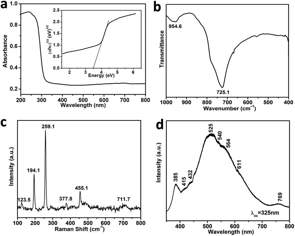 | ||
| Fig. 3 (a) Diffuse reflectance absorption spectrum of the as-prepared Sb2O3 sample. The inset shows the corresponding plots of (αhν)1/2 versus photon energy. (b) Fourier transform infrared spectrum; (c) room-temperature Raman spectrum; (d) photoluminescence spectrum of nest-shaped Sb2O3 micro/nanostructure. | ||
A Raman spectrum for the nest-shaped Sb2O3 material in the range from 100 to 800 cm−1 is shown in Fig. 3c. The strong peaks correspond to Raman shifts of 123.5, 194.1, 259.1, 377.8, 455.1, and 711.7 cm−1. Comparison with previous experimental and theoretical Raman investigations of Sb2O3 (121, 193, 256, 376, 452, 717 cm−1)29 enabled assignment of the main peaks in this spectrum to the cubic Sb2O3 phase. According to previous reports for Sb2O3 materials, the peaks observed for the nest-shaped material can be ascribed to the vibration modes of Sb–O–Sb groups: all signals below 400 cm−1 belong to the external lattice mode regime, whereas those above 400 cm−1 can be ascribed to internal vibration.30
Fig. 3d shows the photoluminescence (PL) spectrum of nest-shaped Sb2O3 using an excitation wavelength of 325 nm. It shows an intense blue emission at 525 nm (2.36 eV), which is associated with oxygen vacancy related defect centers in the Sb2O3 lattice. Deng et al. found that defect centers appeared during the processes of oriented attachment and assisted self-assembly.31 Due to the recombination of photo-generated electrons and holes, a UV emission band at about 385 nm (3.22 eV) was observed. Additional broad peaks at approximately 415, 432, 564 and 611 nm were observed as well and can be attributed to either of the oxygen vacancies, dangling bonds or defect centers.32
In summary, cubic phase Sb2O3 nest-shaped micro/nanostructure has been successfully prepared via a simple wet chemical method in the presence of DDAB. The nest-shaped microparticle has a typical diameter of 5 μm and is composed of nanorods. The formation mechanism of unique nest-shaped micro/nanostructure was attributed to dissolution–recrystallization, self-assembly and oriented attachment process. The UV-vis diffuse reflectance spectrum demonstrates that the band gap energy of as-prepared nest-shaped Sb2O3 is about 3.48 eV, and the PL spectrum reveals an intense blue photoluminescence at 525 nm. These excellent characteristics indicate potential for applications in functional semiconductor materials and photoelectric devices.
Acknowledgements
This project was financially supported by the National Natural Science Foundation of China (No. 51442002).Notes and references
- (a) S. Y. Wei, Q. Wang, J. H. Zhu, L. Y. Sun, H. F. Lin and Z. H. Guo, Nanoscale, 2011, 3, 4474 RSC; (b) Q. L. He, T. T. Yuan, S. Y. Wei, N. Haldolaarachchige, Z. P. Luo, D. P. Young, A. Khasanov and Z. H. Guo, Angew. Chem., Int. Ed., 2012, 51, 8842 CrossRef CAS PubMed; (c) H. G. Wei, Y. R. Wang, J. Guo, N. Z. Shen, D. W. Jiang, X. Zhang, X. R. Yan, J. H. Zhu, Q. Wang, L. Shao, H. F. Lin, S. Y. Wei and Z. H. Guo, J. Mater. Chem. A, 2015, 3, 469 RSC; (d) J. Sharma, M. Lizu, M. Stewart, K. Zygula, Y. Lu, R. Chauhan, X. R. Yan, Z. H. Guo, E. K. Wujcik and S. Y. Wei, Polymers, 2015, 7, 186 CrossRef; (e) J. W. Gu, N. Li, L. D. Tian, Z. Y. Lv and Q. Y. Zhang, RSC Adv., 2015, 5, 36334 RSC; (f) J. W. Gu, J. J. Du, J. Dang, W. C. Geng, S. H. Hu and Q. Y. Zhang, RSC Adv., 2014, 4, 22101 RSC; (g) J. W. Gu, X. T. Yang, Z. Y. Lv, N. Li, C. B. Liang and Q. Y. Zhang, Int. J. Heat Mass Transfer, 2016, 92, 15 CrossRef CAS; (h) S. He, G. S. Wang, J. W. Wang, Y. Z. Wei, Y. Wu, L. Guo and M. S. Cao, ChemPlusChem, 2013, 78, 875 CrossRef CAS; (i) H. Wang, T. T. You, W. W. Shi, J. H. Li and L. Guo, J. Phys. Chem. C, 2012, 116, 6490 CrossRef CAS; (j) H. Wang, J. Gao, T. Q. Guo, R. M. Wang, L. Guo, Y. Liu and J. H. Li, Chem. Commun., 2012, 48, 275 RSC.
- C. Peng, J. J. Guo, W. K. Yang, C. K. Shi, M. R. Liu, Y. X. Zheng, J. Xu, P. Q. Chen, T. T. Huang and Y. Q. Yang, J. Alloys Compd., 2015, 654, 371 CrossRef.
- (a) G. S. Wang, Y. Deng and L. Guo, Chem.–Eur. J., 2010, 16, 10220 CrossRef CAS PubMed; (b) Q. Liu, L. Jiang and L. Guo, Small, 2014, 10, 48 CrossRef CAS PubMed.
- G. C. Qi, S. Z. Zhao and Z. H. Yuan, Sens. Actuators, B, 2013, 184, 143 CrossRef CAS.
- (a) Y. Yang, G. Z. Wang, Y. Liang, C. L. Yuan, T. Yu, Q. L. Li and Q. Li, J. Alloys Compd., 2015, 652, 386 CrossRef CAS; (b) L. L. Lai and J. M. Wu, Ceram. Int., 2015, 41, 12317 CrossRef CAS.
- H. Wang, Y. S. Bai, Q. Wu, W. Zhou, H. Zhang, J. H. Li and L. Guo, Phys. Chem. Chem. Phys., 2011, 13, 7008 RSC.
- P. B. Patil, S. S. Mali, V. V. Kondalkar, R. M. Mane, P. S. Patil, C. K. Hong and P. N. Bhosale, Mater. Lett., 2015, 159, 177 CrossRef CAS.
- (a) J. H. Zhu, S. Y. Wei, M. Alexander, T. D. Dang, T. C. Ho and Z. H. Guo, Adv. Funct. Mater., 2010, 20, 3076 CrossRef CAS; (b) H. G. Wei, X. R. Yan, Y. F. Li, H. B. Gu, S. J. Wu, K. Q. Ding, S. Y. Wei and Z. H. Guo, J. Phys. Chem. C, 2012, 116, 16286 CrossRef CAS; (c) H. G. Wei, D. W. Ding, X. R. Yan, J. Guo, L. Shao, H. R. Chen, L. Y. Sun, H. A. Colorado, S. Y. Wei and Z. H. Guo, Electrochim. Acta, 2014, 132, 58 CrossRef CAS.
- H. Wang, Q. Q. Liang, W. J. Wang, Y. R. An, J. H. Li and L. Guo, Cryst. Growth Des., 2011, 11, 2942 CAS.
- L. Jiang, P. G. Yin, T. T. You, H. Wang, X. F. Lang, L. Guo and S. H. Yang, ChemPhysChem, 2012, 13, 3932 CrossRef CAS PubMed.
- L. Jiang, T. T. You, P. G. Yin, Y. Shang, D. F. Zhang, L. Guo and S. H. Yang, Nanoscale, 2013, 5, 2784 RSC.
- W. H. Fan, Z. W. Shi, X. P. Yang, M. M. Cui, X. L. Wang, D. F. Zhang, H. Liu and L. Guo, Water Res., 2012, 46, 5981 CrossRef CAS PubMed.
- Y. Shang and L. Guo, Adv. Sci., 2015, 2, 1500140 CrossRef.
- (a) A. Laachachi, M. Cochez, M. Ferriol, E. Leroy, J. M. Lopez Cuesta and N. Oget, Polym. Degrad. Stab., 2004, 85, 641 CrossRef CAS; (b) Z. J. Dong, L. R. Xun and F. S. Hua, J. Cent. South Univ. T., 2008, 15, 64 CrossRef; (c) E. Jakab, M. A. Uddin, T. Bhaskar and Y. Sakata, J. Anal. Appl. Pyrolysis, 2003, 68, 83 CrossRef; (d) M. Brebu, E. Jakab and Y. Sakata, J. Anal. Appl. Pyrolysis, 2007, 79, 346 CrossRef.
- (a) K. Matsuzawa, A. T. Shido and Y. Iwasawa, Langmuir, 2003, 19, 2756 CrossRef CAS; (b) B. Duh, Polymer, 2002, 43, 3147 CrossRef CAS; (c) J. Spengler, F. Anderle, E. Bosch, R. K. Grasselli, B. Pillep, P. Behrens, O. B. Lapina, A. A. Shubin, A. H. J. Eberle and H. Knözinger, J. Phys. Chem. B, 2001, 105, 10772 CrossRef CAS; (d) H. C. Liu and Y. Iwasawa, J. Phys. Chem. B, 2002, 106, 2319 CrossRef CAS.
- (a) P. W. Haycock, G. A. Horley, K. C. Molloy, C. P. Myers, S. A. Rushworth and L. M. Smith, J. Phys. IV, 2001, 11, 1045 Search PubMed; (b) T. S. Zhang, P. Hing and R. F. Zhang, J. Mater. Sci., 2000, 35, 1419 CrossRef.
- (a) V. Aravindan and P. Vickraman, Solid State Sci., 2007, 9, 1069 CrossRef CAS; (b) M. Legouera, P. Kostka and M. Poulain, J. Phys. Chem. Solids, 2004, 65, 901 CrossRef CAS; (c) R. E. Youngman, S. Sen, L. K. Cornelius and A. J. G. Ellison, Phys. Chem. Glasses, 2003, 44, 69 CAS.
- K. S. Liu, Z. Jin and J. Lei, Nanotechnology, 2008, 19, 6588 Search PubMed.
- L. M. Song, S. J. Zhang and Q. W. Wei, Chem. Eng. J., 2012, 179, 404 CrossRef CAS.
- S. S. Ge, X. K. Yang, Q. Shao, Q. Y. Liu, T. J. Wang, L. Y. Wang and X. J. Wang, J. Solid State Chem., 2013, 200, 136 CrossRef CAS.
- S. S. Ge, Q. Y. Wang, J. Y. Li, Q. Shao and X. J. Wang, J. Alloys Compd., 2010, 494, 169 CrossRef CAS.
- (a) L. M. Song, S. J. Zhang and Q. W. Wei, Cryst. Growth Des., 2012, 12, 764 CrossRef CAS; (b) L. Liu, Z. L. Hu, Y. M. Cui, B. Li and X. F. Zhou, Solid State Sci., 2010, 12, 882 CrossRef CAS.
- J. Zhou, H. W. Zhao and L. Guo, Chin. Sci. Bull., 2014, 59, 572 CrossRef.
- H. Gleiter, Int. Mater. Rev., 1995, 40, 41 CrossRef.
- T. Kunitake and Y. Okahata, J. Am. Chem. Soc., 1977, 99, 3860 CrossRef CAS.
- S. S. Ge, Q. Y. Wang, Q. Shao, Y. H. Zhao, X. K. Yang and X. J. Wang, Appl. Surf. Sci., 2011, 257, 3657 CrossRef CAS.
- X. Zhang, X. R. Yan, Q. L. He, H. G. Wei, J. Long, J. Guo, H. B. Gu, J. F. Yu, J. J. Liu, D. W. Ding, L. Y. Sun, S. Y. Wei and Z. H. Guo, ACS Appl. Mater. Interfaces, 2015, 7, 6125 CAS.
- (a) A. E. Panasenko, L. A. Zemnukhova, L. N. Ignat'eva, T. A. Kaidalova, S. I. Kuznetsov, N. V. Polyakova and Y. V. Marchenko, Inorg. Mater., 2009, 45, 402 CrossRef CAS; (b) A. H. Abdullah, N. H. M. Noor, I. Ramli and M. Hashim, Mater. Chem. Phys., 2008, 111, 201 CrossRef CAS.
- (a) I. A. Degen and G. A. Newman, Spectrochim. Acta, Part A, 1993, 49, 859 CrossRef; (b) X. C. Ma, Z. D. Zhang, X. B. Li, Y. Du, F. Xu and Y. T. Qian, J. Solid State Chem., 2004, 177, 3824 CrossRef CAS.
- B. S. Naidu, M. Pandey, V. Sudarsan, R. Tewari and R. K. Vatsa, J. Lumin., 2011, 131, 177 CrossRef CAS.
- Z. T. Deng, D. Chen, F. Q. Tang, X. W. Meng, J. Ren and L. Zhang, J. Phys. Chem. C, 2007, 111, 5325 CAS.
- Q. Y. Wang, X. C. Yang, J. W. Hou, M. Huang and Y. H. Zhao, Appl. Surf. Sci., 2011, 257, 5857 CrossRef CAS.
Footnote |
| † Electronic supplementary information (ESI) available: Synthetic process and mechanism analysis. See DOI: 10.1039/c6ra20558e |
| This journal is © The Royal Society of Chemistry 2016 |