
Phosphonic acid self-assembled monolayer improved the properties of n-type organic field-effect transistors in air ambient†
Li Cao,
Yue Peng and
Zhefeng Li*
College of Chemistry and Chemical Engineering, Chongqing University, Chongqing 400044, PR China. E-mail: zhefeng@cqu.edu.cn
First published on 13th September 2016
Abstract
Here we report an approach to surface modification of the SiO2 gate dielectric on a Si device based on a simple procedure in which a dilute solution of a phosphonic acid is drawn down across the surface of the Si substrate. A crystalline thin film of NDI-C14 was successfully grown by vapor deposition on the surface of SAM modified dielectrics and obtained improved electron mobility up to 4.23 × 10⁻² cm2 V−1 s−1 at room temperature in air ambient. Three SAM (ODPA, TDPA, and NAPA) modified dielectrics increased the electron mobility of the NDI-C14 by three orders of magnitude compared to that on bare SiO2. The improvement of electron mobility is associated with the close packing arrangement of NDI-C14 film on different SAMs.
Introduction
Organic semiconductors are the active components of organic thin film transistors (OTFTs) that include n-type (electron-transporting) and p-type (hole-transporting). Although a number of n-type organic semiconductor materials have been advanced for OTFT applications, there is still an urgent need for further improvement in not only device performance but also other factors such as air stability and thin-film morphology.1–4 Naphthalene diimides (NDIs) are among the most representative n-channel materials for organic TFTs because of their high electron affinity and easily controllable properties by changing the substituent on the imide N atoms or on the naphthalene backbone.5–7 Especially, N,N′-dialkyl-1,4,5,8-naphthalenediimides (NDI-Cn) are extremely promising n-type materials with a high electron mobility, and air stability.8 For instance, Deepak et al. have reported that vapor-deposited OTFTs based on N,N-bis(cyclohexyl)naphthalene diimides (NDI) exhibited high electron mobilities.9,10 Musubu et al. have synthesized several corecyanated NDIs (NDI-C8, NDI-C11, NDI-C12, NDI-C13, NDI-C15, NDI-C18) with different length alkyl chains.11,12 Numerous researchers have made efforts to develop high-mobility n-type NDI OTFTs by modifying the substituent on the imide N atoms, by controlling deposition conditions and modifying the surface state of the dielectrics with self-assembled monolayers (SAMs).13It is universally acknowledged that the morphology and microstructure of organic thin film has a strong impact on the charge carrier mobility and OTFTs device characteristics. Generally, the surfaces of these dielectric structures post-fabrication are commonly partially covered with –OH groups leading to reduced performance in organic devices fabricated on this unmodified layer.14,15 An effective method to block charge traps and provide a smooth transition from an inorganic dielectric material to an organic semiconductor is through the use of self-assembly.16,17 Silane based molecules and phosphonic acid (PA) based molecules are commonly used to modify silicon substrate surfaces. However, compared with silane SAMs, PA SAMs have better stability to moisture and less tendency to homocondense between self-assembled molecules.18,19 The PA head group has a better affinity for the SiO2 and begins forming covalent bonds with the SiO2 substrate surface immediately after exposure.20 Clearly, PA SAMs with tremendous potential to optimize insulator/semiconductor interface of OTFTs that would be taken priority of selection.
In this research, we report air stable N,N′-bis(n-tetradecyl)-1,4,5,8-naphthalene diimide (NDI-C14)-based bottom-gate top-contact n-type OTFTs, which modified by three kinds of PA SAMs molecules octadecyl phosphonic acid (ODPA), tetradecyl phosphonic acid (TDPA), and 6-naphthoxy-hexyl phosphonic acid (NAPA). Although, NDI derivatives bearing normal alkyl chains with various lengths have been reported a lot, we believe that there are currently no reports that NDI-C14-based OTFTs with good performance. The unmodified OTFT exhibit fairly weak performance of semiconductor, and it's electron mobility as low as 1.17 × 10⁻⁵ cm2 V−1 s−1 from our experiment. Oppositely, the three PA SAMs of OTFTs exhibit relatively high electron mobility, that ODPA SAMs shows the optimum mobilities up to 4.23 × 10⁻² cm2 V−1 s−1 at room temperature in air ambient. It is observed that the electron mobility enhanced highly significant. By study the morphology of NDI-C14 film on different SAMs, it is found that the improvement of electron mobility is associated with its close packing arrangement of NDI-C14 film on different SAMs.
Experimental
Synthesis of NDI-C14
NDI-C14 was synthesized by condensation of naphthalene dianhydride with tetradecylamine. A mixture of 1,4,5,8-naphalenetetracarboxylic acid anhydride (0.5 g, 1.8 mmol), tetradecylamine (2.3 g, 10.8 mmol) and zinc acetate (50 mg) in 70 mL NMP was heated at 120 °C for 6 hours. The mixture was cooled and diluted with several volumes of methanol. The resulting slurry was filtered, the collected solid washed with methanol and dried in air. The crude product was then purified by column chromatography using dichloromethane as eluent (yield: 79%). 1H NMR (500 MHz, CDCl3): δ = 8.75 (s, 4H), 4.18–4.21 (t, 4H), 1.25 (s, 48H), 0.87 (d, 6H). Calcd for C42H62N2O4: C, 76.55%; H, 9.48%; N, 4.25%. Found: C, 76.36%; H, 9.57%; N, 4.21%.SiO2 surface modification with ODPA
An oxidized silicon wafer (Si is highly n-doped with resistivity smaller than 0.005 G cm and the thermally grown SiO2 is 300 nm thick) was used as substrates for organic thin film transistors. The following surface treatments of the SiO2 were performed on the dielectric surface before vacuum sublimation of the semiconductor film: a 10 min sonication in acetone, followed by a 70![[thin space (1/6-em)]](https://www.rsc.org/images/entities/char_2009.gif) :30 H2SO4/H2O2 (piranha) etch for 1 hour at 100 °C, then a 1:1:5 NH3 H2O/H2O2/deionized H2O wash for 20 min at 70 °C, and the silicon wafer was held vertically using a small clamp in a solution of ODPA (1 mM in THF) in a 50 mL beaker. The solvent was allowed to evaporate slowly over 3 h, until the level of the solution fell below the silicon wafer. The treated Si sample was then removed from its holder and was heated at 140 °C in a simple glass tube for 2 days to bond the SAMs to the SiO2/Si as octadecylphosphonate. ODPA/SiO2/Si substrate was sonicated in THF for 10 min. NAPA and TDPA modified SiO2 wafers were made with the same method.
:30 H2SO4/H2O2 (piranha) etch for 1 hour at 100 °C, then a 1:1:5 NH3 H2O/H2O2/deionized H2O wash for 20 min at 70 °C, and the silicon wafer was held vertically using a small clamp in a solution of ODPA (1 mM in THF) in a 50 mL beaker. The solvent was allowed to evaporate slowly over 3 h, until the level of the solution fell below the silicon wafer. The treated Si sample was then removed from its holder and was heated at 140 °C in a simple glass tube for 2 days to bond the SAMs to the SiO2/Si as octadecylphosphonate. ODPA/SiO2/Si substrate was sonicated in THF for 10 min. NAPA and TDPA modified SiO2 wafers were made with the same method.
Fabrication of OFETs devices
The thin films composed of NDI-C14 was vacuum-deposited by an TECHNOL ZHD-300 vacuum coater with the Turbo-molecular pump at a pressure of 9.0 × 10⁻⁶ Torr or lower, with a deposition rate of ca. 0.1 Å s−1 to the desired thickness. The temperature of substrate was 25 °C for NDI-C14. During vacuum deposition the distance between source and substrate was 18 cm. Different substrate temperatures for deposition were achieved using a radiant heater and measured with a thermocouple. Top-contact drain and source gold electrodes were vacuum-deposited through a shadow mask onto the films of NDI-C14 in the same vacuum chamber, and the resulting semiconducting channels were 50 μm (L) × 2 mm (W) and 100 μm (L) × 2 mm (W). In these transistors highly n-doped silicon functioned as gate electrode and SiO2 of 300 nm thick (untreated or treated with SAMs) functioned as dielectrics.Characterization and apparatus
1H NMR spectra (500 MHz) were taken on a Bruker 500 ultra-shield NMR spectrometer with tetramethylsilane (TMS) as internal reference. Elemental analyses of carbon, hydrogen, and nitrogen were performed on a Vario-EL analyzer. Cyclic voltammetry (CV) investigations of the synthesized NDI-C14 were carried out using an electrochemical workstation (CHI 660E). Thermal gravity analysis (TGA) was performed on a Simultaneous Thermal Analyzer DTG-60H under nitrogen at a heating rate of 10 °C min−1. Morphology of NDI-C14 films were investigated by Atomic Force Microscope (AFM, Jpk nano wizard 2). XRD of organic semiconductor films were measured on a diffractometer LabX XRD-6000. Electrical measurements of OTFTs were taken on KEITHLEY 4200 semiconductor system in ambient atmosphere.Results and discussion
The compounds and device structure of (NDI-C14)-based bottom-gate top-contact n-type OTFTs were shown in Fig. 1. For n-type OTFTs, the thermal stability of organic semiconductors materials (OSCs) are very significant since they are directly related to practical issues such as device fabrication and operation. | ||
| Fig. 1 Chemical structure of NDI-C14, SAMs molecules and schematic cross section of TFTs prepared in this study. | ||
The NDI-C14 was thermally stable up to 385 °C and complete degradation is observed above 460 °C (ESI Fig. 1†). The maximum deposition temperature is ∼220 °C, which is much below the degradation temperature of NDI-C14.
Cyclic voltammogram of NDI-C14 was shown in Fig. 2. For measurements, glassy carbon electrode as working electrode, Pt electrode as counter electrode, Ag/AgCl electrode as reference electrode were used. NDI-C14 was dissolved in 0.1 M dichloromethane chloride solution of TBPAF6 which used as supporting electrolyte. The concentration of NDI-C14 was 1.28 × 10⁻⁴ M, and at a scan rate of 50 mV s−1. Its reduction potentials was measured to be  = −0.66 V and
  = −0.74 V. Accordingly, the LUMO energy was obtained from the following eqn (1)
 | (1) |
 and
and  are the half-wave reduction potentials. Eref is a reference electrode position relative to the vacuum level. For the Ag/AgCl electrode, the Eref value is equal to −4.7 eV. The LUMO energy of NDI-C14 was estimated to be −3.99 eV. Compared to that of NDI without substituent, the LUMO energies of NDI-C14 is lowered by 0.1 eV.
 | ||
| Fig. 2 Cyclic voltammogram of NDI-C14. | ||
Thin film transistors of NDI-C14 acted as semiconductor layer and three type SAMs (ODPA, TDPA and NAPA) were used to modified dielectric layer presented n-channel semiconductor characteristic, while the OTFTs on bare SiO2 did not exhibit obvious field effect properties. The transistors key parameters (μ, Vth, Ion/off) with various SAMs are summarized in Table 1. NDI-C14 on ODPA-modified substrates exhibited an electron mobility as high as 4.23 × 10⁻² cm2 V−1 s−1 along with an on/off ratio of 6.20 × 10³ and a threshold voltage (Vth = 16 V). In comparison, NDI-C14 on TDPA and NAPA modified substrates shown a little lower electron mobility of 1.29 × 10⁻² to 3.80 × 10⁻² cm2 V−1 s−1. Obviously, SAMs modified dielectrics not only increased the electron mobility and on/off ratio of the NDI-C14 by three orders of magnitude but also improved the threshold voltage and air-stability.
| Compound | Ts (°C) | Dielectric surface | μ (cm2 V−1 s−1) | Vth (V) | Ion/off |
|---|---|---|---|---|---|
| NDI-C14 | RT (25 °C) | SiO2 | 1.17 × 10⁻⁵ | 18 | 1.2 × 10² |
| NAPA/SiO2 | 1.29 × 10⁻² | 15 | 1.43 × 10³ | ||
| TDPA/SiO2 | 3.80 × 10⁻² | 22 | 7.54 × 10³ | ||
| ODPA/SiO2 | 4.23 × 10⁻² | 16 | 6.20 × 10³ |
The output curves and transfer curves of NDI-C14/ODPA/SiO2, NDI-C14/TDPA/SiO2 and NDI-14/NAPA/SiO2 were given in Fig. 3a–c. The mobility of the saturated region was extracted from the following eqn (2)
 | (2) |
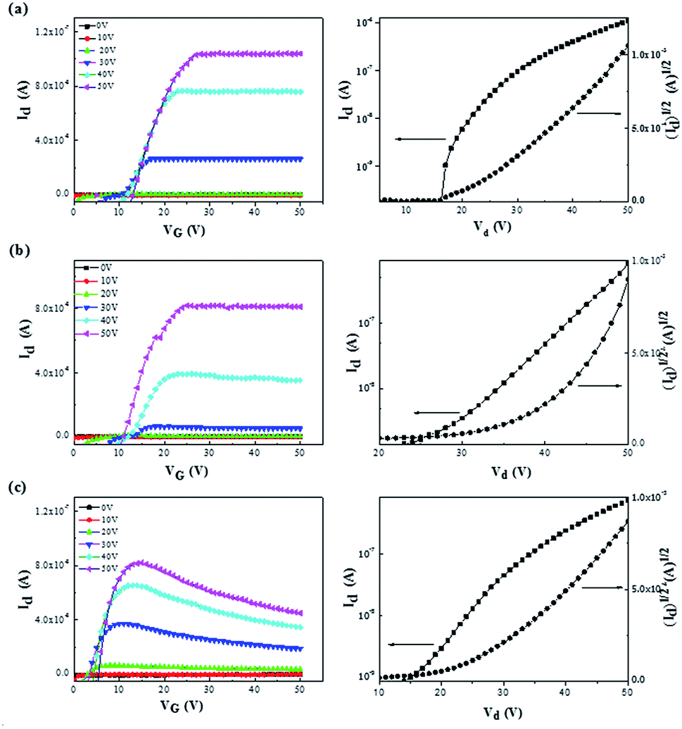 | ||
| Fig. 3 Output and transfer characteristics curves of (a) NDI-C14/ODPA, (b) NDI-C14/TDPA, (c) NDI-C14/NAPA. | ||
To understand the role of SAMs in the induced crystallization of NDI-C14, AFM images of 60 nm thick NDI-C14 films on the different SAMs surfaces were investigated using AFM. As shown in Fig. 4 and 5, the thin-film morphology of NDI-C14 on ODPA/SiO2 and TDPA/SiO2 are composed of uniform and well-connected height circular grains associated with island growth mode. Also, it can be seen on Fig. 5a and b, the circular grains of NDI-C14 on ODPA/SiO2 is bigger than that of NDI-C14 on TDPA/SiO2. While NDI-C14 on bare SiO2 has poorly connected 3D grains with open grain boundaries that extend down to the underlying substrate. The 3D image of NDI-C14 film on NDPA/SiO2 is similar to that on bare SiO2.
 | ||
| Fig. 4 AFM height images (10 μm scale) of 80 nm NDI-C14 film on (a) ODPA/SiO2, (b) TDPA/SiO2, (c) NAPA/SiO2 surfaces and (d) bare SiO2 surface. | ||
 | ||
| Fig. 5 AFM 3D images (10 μm scale) of 80 nm NDI-C14 film on (a) ODPA/SiO2, (b) TDPA/SiO2, (c) NAPA/SiO2 surfaces and (d) bare SiO2 surface. | ||
The compact morphology of NDI-C14 on ODPA/SiO2 and TDPA/SiO2 may provide a continuous percolation pathway for electron accumulation and transport which in turn prevents high charge density accumulation at the dielectric interface.21
The improvement in the charge carrier mobility using any one of the SAMs compared to the bare SiO2 can be explained in part from a combination of surface energy and chemical functionality at the dielectric interface.22 This is helpful for NDI-C14 film to form close packing arrangement when deposition in vacuum.
From the X-ray diffraction analysis (XRD), it can be confirmed that NDI-C14 form crystal thin films on four different surfaces (ODPA, TDPA, NAPA and bare SiO2) and show major peaks at 2θ = 5.8° (d spacing = 15.4 Å) and 2θ = 8.6° (d spacing = 10.4 Å) (shown in Fig. 6). The diffraction peaks are consistent with other NDI derivatives which have been reported.23,24
 | ||
| Fig. 6 X-ray diffraction patterns of 80 nm thick NDI-C14 films on different surfaces. | ||
Conclusions
In conclusion, we have definitely demonstrated a new strategy of using three SAMs (ODPA, TDPA, and NAPA) to modify SiO2 dielectrics. It shows that SAMs layer possess multiple properties known to be beneficial for device performance, such as dipole moment, high hole/electron conductivity, and hole/electron blocking effects, have tremendous potential for further improvement of organic electronic devices. The three SAMs can induce NDI-C14 to form orderly crystal thin film during vapor deposition. The best device shows FET of 4.23 × 10⁻² cm2 V−1 s−1, threshold voltage of 16 V, on/off current ratio of 6.2 × 10³. From AFM morphology studying, it is found that SAMs-treated SiO2 is helpful for improving growth of the organic semiconductor with fewer defects, and higher local order. This in turn maximizes the charge carrier mobility of the whole device. Thus, appropriate surface modification at dielectric interfaces is essential for enhancing the electrical properties of organic thin film transistors.Acknowledgements
Financial aid from the Opening fund of State Key Laboratory of Rare Earth Resources Utilization (No. RERU2015011), and the Fundamental Research Funds for the Central Universities (No. CDJZR13225502 and CDJRC10220007) are gratefully acknowledged.Notes and references
- H. Chang, Y. Deng, Y. Geng, T. Wang and D. Yan, Org. Electron., 2015, 22, 86–91 CrossRef CAS.
- Z. Yuan, Y. Ma, T. Gebner, M. Li, L. Chen and M. Eustachi, Org. Lett., 2016, 18, 456–459 CrossRef CAS PubMed.
- T. He, M. Stolte and F. Wurthner, Adv. Mater., 2013, 25, 6951–6955 CrossRef CAS PubMed.
- R. A. Street, Adv. Mater., 2009, 21, 4173 CrossRef.
- Y. Wen, Y. Liu, C.-A. Di, Y. wang, X. Sun, Y. Guo and J. Zheng, Adv. Mater., 2009, 21, 1631 CrossRef CAS.
- X. Li, C. Xiao, W. Jiang and Z. Wang, J. Mater. Chem. C, 2013, 1, 7513 RSC.
- H. E. Katz, J. Johnson, A. J. Lovinger and W. Li, J. Am. Chem. Soc., 2000, 122, 7787–7792 CrossRef CAS.
- J. H. Oh, S. L. Suraru, W.-Y. Lee, M. Konemann, H. W. Hoffken, C. Roger, R. Schmidt, Y. Chung, W.-C. Chen and Z. Bao, Adv. Funct. Mater., 2010, 20, 2148 CrossRef CAS.
- B. A. Jones, A. Facchetti, T. J. Marks and M. R. Wasielewski, Chem. Mater., 2007, 19, 2703 CrossRef CAS.
- D. Shukla, S. F. Nelson, D. C. Freeman, M. Rajeswaran, W. G. Ahearn, D. M. Meyer and J. T. Carey, Chem. Mater., 2008, 20, 7486–7491 CrossRef CAS.
- I. Tszydel, M. Kucinska, T. Marszalek, R. Rybakiewicz, A. Nosal, J. Jung, M. Gazicki-Lipman and J. Ulanski, Adv. Funct. Mater., 2012, 22, 3840 CrossRef CAS.
- M. Ichikawa, Y. Yokoka, H.-G. Jeon, G. R. Banoukepa, N. Hirata and N. Oguma, Org. Electron., 2013, 14, 516–522 CrossRef CAS.
- T. Jung, B. Yoo, L. Wang, A. Dodabalapur, B. A. Jones, A. Facchetti, M. R. Wasielewski and T. J. Marks, Appl. Phys. Lett., 2006, 88, 183102 CrossRef.
- B. A. Jones, A. Facchetti, M. R. Wasielewski and T. J. Marks, J. Am. Chem. Soc., 2007, 129, 15259–15278 CrossRef CAS PubMed.
- M. McDowell, I. G. Hill, J. E. McDermott, S. L. Bernasek and J. Schwartz, Appl. Phys. Lett., 2006, 88, 073505 CrossRef.
- D. O. Hutchins, T. Weidner, J. Baio, B. Polishak, O. Acton, N. Cernetic, H. Ma and A. K.-Y. Jen, J. Mater. Chem. C, 2013, 1, 101 RSC.
- O. Acton, I. Osaka, G. Ting, D. O. Hutchins, H. Ma, R. D. McCullough and A. K. Y. Jen, Appl. Phys. Lett., 2009, 95, 113305 CrossRef.
- P. Thessen, M. Valtiner and G. Grundmeier, Langmuir, 2009, 26, 156 CrossRef PubMed.
- M. Novak, A. Ebel, T. Meyer-Friedrichsen, A. Jedaa, B. F. Vieweg, G. Yang, K. Voitchovsky, F. Stellacci and E. Spiecker, Nano Lett., 2010, 11, 156 CrossRef PubMed.
- E. L. Hanson, J. Schwartz, B. Nickel, N. Koch and M. F. Danisman, J. Am. Chem. Soc., 2003, 125, 16074–16080 CrossRef CAS PubMed.
- M. S. Liu, Y. J. Cheng and G. Ting, Adv. Funct. Mater., 2008, 18, 3964–3971 CrossRef.
- H. Ma, O. Acton, D. O. Hutchins, N. Cernetic and A. K.-Y. Jen, Phys. Chem. Chem. Phys., 2012, 14, 14110–14126 RSC.
- P. Gawrys, D. Boudinet, M. Zagorska, D. Djurado, J. M. Verilhac, G. Horowitz, J. Pécaud, S. Pouget and A. Pron, Synth. Met., 2009, 159, 1478–1485 CrossRef CAS.
- A. Kalita, A. Dey and P. Krishnan Iyer, Phys. Chem. Chem. Phys., 2016, 18, 12163–12168 RSC.
Footnote |
| † Electronic supplementary information (ESI) available. See DOI: 10.1039/c6ra17255e |
| This journal is © The Royal Society of Chemistry 2016 |