
 Open Access Article
 This Open Access Article is licensed under a
 Creative Commons Attribution 3.0 Unported Licence
Effect of sulfur substitution on the thermoelectric properties of (SnSe)1.16NbSe2: charge transfer in a misfit layered structure
Priyanka
Jood
* and
Michihiro
Ohta
 *
*
Research Institute for Energy Conservation, National Institute of Advanced Industrial Science and Technology (AIST), 1-1-1 Umezono, Tsukuba, Ibaraki 305-8568, Japan. E-mail: p.jood@aist.go.jp; ohta.michihiro@aist.go.jp
First published on 31st October 2016
Abstract
Misfit layered compounds have gained tremendous interest in the past couple of years due to the unique opportunities they offer for ZT enhancement arising from their phonon glass-electron crystal (PGEC) behavior. In this study we investigated the thermoelectric properties of polycrystalline layered misfit selenide (SnSe)1.16NbSe2 for the first time and tried to optimize its high hole concentration (p ∼ 9.6 × 1021 cm−3) through sulfur (S) doping. The Seebeck coefficient, electrical resistivity, and thermal conductivity were measured in both directions, perpendicular (in-plane) and parallel (out-of-plane) to the pressing direction over the temperature range of 300 K to 760 K. S doping resulted in the decrease of hole concentration (p ∼ 4.0 × 1021 cm−3) and ∼50% increase in hole mobility by increasing the charge transfer from SnSe to NbSe2 layer. This provided a 15% enhancement in power factor over the entire temperature range with a value of ∼120 μW K−2 m−1 at 760 K in the out-of-plane direction. These power factor values are still quite low for this misfit to be considered as a potential thermoelectric material. Further p optimization needs to be performed through charge transfer tuning in order to increase the power factor. For all the samples, the κlat is quite low and lies in the range from 0.9 to 2.3 W K−1 m−1 in the out-of-plane direction at 760 K. Despite such low κlat, this Se misfit shows a poor maximum ZT (∼0.03 at 760 K) owing to high carrier concentration (low power factor). Nonetheless, this work provides further insights into the interdependence of electrical properties and charge transfer in misfit systems.
1. Introduction
There is an ever increasing demand for sustainable clean energy technologies to overcome the energy crisis and to provide a promising solution to the global climate change. Thermoelectric power generation is one such technology that has been generating extensive interest, since it involves power generation from waste heat produced by various sources such as, automobiles, power plants, data centres etc. The efficiency of a thermoelectric device largely depends on the potential of the comprising p and n-type thermoelectric materials, which in turn is determined by their dimensionless thermoelectric figure of merit, ZT= (S2/ρκtotal)T, where S, ρ, κtotal, and T are Seebeck coefficient, electrical resistivity, total thermal conductivity (κtotal = κel + κlat; κel is electronic thermal conductivity and κlat is lattice thermal conductivity) and absolute temperature.Many new concepts have been proposed to guide the search for novel thermoelectric materials and phonon glass-electron crystal (PGEC) concept1 is among the prominent ones. In a PGEC material, the phonon glass region provides the disorder needed for phonon scattering (i.e., low κlatl) without affecting the carrier mobility in the electron crystal region (i.e., high S2/ρ), providing a perfect platform for ZT optimization. The most known examples of PGEC materials include filled skutterudites2 and clathrates3 consisting of rattling atoms, tetrahedrites with low energy vibration modes,4 nanocomposites consisting of coherently embedded nanoprecipitates,5–7 and layered systems such as superlattice thin films8 and layered oxides and chalcogenides9–13 where one layer serves as a carrier pathway and the other provides disorder. Misfit layered oxides such as NaxCoO2![[thin space (1/6-em)]](https://www.rsc.org/images/entities/char_2009.gif) 9,14 and Ca–Co–O10,11 have shown promising high temperature thermoelectric properties, however, their high electrical resistivity due to high electronegativity of oxygen still poses a limit for ZT enhancement. This brought misfit layered sulfides to the attention of the thermoelectric community since one can expect better power factor (S2/ρ) owing to their lower electrical resistivity compared to oxides.15 Misfit layered sulfides are a part of the family (MX)1+m(TX2)n (M = Pb, Bi, Sn, Sb, rare-earth elements; T = Ti, V, Cr, Nb, Ta; X = S, Se; n = 1, 2, 3)16,17 and provide tremendous opportunities for ZT enhancement due to their PGEC behavior, where the CdI2-type TX2 host layer provides a passage for high-mobility carrier and the intercalated NaCl-type MX layer creates disorder and is responsible for scattering phonons. The charge transfer from MX to TX2 layer maintains the stability of the whole system.
9,14 and Ca–Co–O10,11 have shown promising high temperature thermoelectric properties, however, their high electrical resistivity due to high electronegativity of oxygen still poses a limit for ZT enhancement. This brought misfit layered sulfides to the attention of the thermoelectric community since one can expect better power factor (S2/ρ) owing to their lower electrical resistivity compared to oxides.15 Misfit layered sulfides are a part of the family (MX)1+m(TX2)n (M = Pb, Bi, Sn, Sb, rare-earth elements; T = Ti, V, Cr, Nb, Ta; X = S, Se; n = 1, 2, 3)16,17 and provide tremendous opportunities for ZT enhancement due to their PGEC behavior, where the CdI2-type TX2 host layer provides a passage for high-mobility carrier and the intercalated NaCl-type MX layer creates disorder and is responsible for scattering phonons. The charge transfer from MX to TX2 layer maintains the stability of the whole system.
The discovery of a large power factor ∼3710 μW K−2 m−1 in TiS2 single crystal18,19 along with a high κtotal ∼ 6.7 W K−1 m−1 triggered an extensive research on its intercalated compounds where the guest transition metals or rock-salt-type MS layers (where M = Pb, Bi, or Sn) were intercalated into the van der Waals gap of layered TiS2, with the aim of lowering its κlat.20–23 Promising ZT values were reported for various intercalated sulfides such as, n-type ZT ≈ 0.45 at 800 K for polycrystalline Cu0.02TiS2,21 n-type ZT ≈ 0.38 at 673 K for polycrystalline (SnS)1.2(TiS2)2,20 p-type ZT ≈ 0.2 at 950 K for (La1.05S1.05)1.14NbS2,24 and n-type ZT ≈ 0.14 at 950 K for (LaS)1.20CrS2.25 Recently, organic intercalation has also been achieved in layered TiS2 in order to form a flexible hybrid superlattice with ZT of 0.28 at 373 K.26 These studies show the potential of layered misfit sulfides as new generation thermoelectric materials. Layered misfit selenides, however, have not been explored yet for their temperature dependent thermoelectric performance.
In this study, we present an in-depth account of the high temperature thermoelectric properties of (SnSe)1.16NbSe2 or Sn1.16NbSe3.16 misfit selenide. This compound has been studied by a few authors in the past for various aspects, such as, (1) its complex crystal structure27 which ensures low lattice thermal conductive like all other misfit layered chalcogenides, (2) synthesis and study of ferecrystalline alloys/thin films28–30 which have shown that charge transfer and hence the electronic properties in this misfit are tunable and, (3) polycrystalline room temperature electronic properties16,27 which indicate its low room temperature electrical resistivity (∼6 μΩ m). These previous studies make this misfit selenium compound a suitable candidate for thermoelectric investigation as well. In this study we also try to improve the thermoelectric performance of Sn1.16NbSe3.16 misfit selenide by doping the Se site with S. Presence of mixed anion/cation have proven to be beneficial in terms of enhancing ZT31 and influencing the interlayer/intralayer interactions32 for similar systems in the past.
2. Experimental
2.1 Synthesis and sintering
Elemental tin (Sn; 99.9999%, Kojundo Chemical Laboratory Co. Ltd), elemental niobium (Nb; 99.9%, Kojundo Chemical Laboratory Co. Ltd), elemental selenium (Se; 99.999%, Kojundo Chemical Laboratory Co. Ltd), and elemental sulfur (S; 99.9999%, Kojundo Chemical Laboratory Co. Ltd) were used as starting materials without further purification. Powders (∼6 g) with nominal composition Sn1.16Nb(Se1−xSx)3.16 (x = 0, 0.1, 0.2) were synthesized by mixing appropriate ratios of starting materials of Sn, Nb, Se, and S in quartz tubes. For example, 1.775 g of Sn, 1.197 g of Nb, 2.895 g of Se, and 0.130 g of S were used to prepare 6 g of Sn1.16Nb(Se0.9S0.1)3.16. The tubes were evacuated to 7 × 10⁻³ Pa and then sealed. They were heated to 673 K at a rate of 0.5 K min−1 and held for 12 h, and further heated to 1023 K and held for 24 h. The samples were then cooled to room temperature over 12 h. The prepared powders were grinded and placed into 10 mm- or 15 mm-diameter graphite dies which were then inserted into the sintering equipment (SPS-515S, Fuji Electronic Industrial) and heated at 14 K min−1. Sintering was performed at 923 K for 1 h under 30 MPa uniaxial pressure in vacuum (7 × 10⁻³ Pa) and subsequently cooled at 25 K min−1 to prepare high density and oriented sintered compacts, which were cut into bars, disks, and plates for further measurements. The density of the sintered compacts was determined using the gas pycnometer method (Accu Pyc II 1340, Shimadzu) at room temperature. All samples showed a density >95% of the theoretical density.2.2 Powder X-ray diffraction and scanning electron microscopy
The crystal structure of the powders and the grain orientation in the sintered compacts was examined using XRD (Rint-Ultima+, Rigaku) with Cu Kα radiation over the 2θ range of 10–60°. Lattice parameters were refined by Le Bail decomposition to the powder XRD data using JANA2006 software.33The microstructure of the sintered compacts were observed using scanning electron microscopy (SEM, HITACHI, TM3030 Plus, Miniscope).
2.3 Electrical transport measurement
The Seebeck coefficient and electrical resistivity of the compact samples were simultaneously measured using temperature-differential and four probe methods, respectively, (ZEM-3, Advance Riko) perpendicular (in-plane) and parallel (out-of-plane) to the pressing direction under a He atmosphere over the temperature range of 300–773 K. The bars used for the in-plane and out-of-plane measurements typically were ∼3 mm × ∼2 mm × ∼10 mm and ∼3 mm × ∼2 mm × ∼7 mm, respectively. Seebeck coefficient and electrical resistivity were reproducible over heating and cooling cycles for both directions. The uncertainty of the Seebeck coefficient and electrical conductivity is estimated to be within ∼5%.The Hall coefficient of the sintered compacts was measured using a homemade system under a magnetic field from 0 to 2.3 T at room temperature. The samples typically were ∼5 mm × ∼5 mm × ∼0.3 mm. In rich In–Ga paste was used to attach Cu contact wires to the samples. In our previous work we have confirmed the accuracy of our home made Hall measurement system by measuring the same samples using physical property measurement system (PPMS, Quantum Design).25
2.4 Thermal transport measurement
The total thermal conductivity (κtotal) was calculated using the density (d), the thermal diffusivity (D), the heat capacity (CP) of the sintered compacts, and the equation κtotal = DCPd. The thermal diffusivity was directly measured and the heat capacity was indirectly derived using a standard sample (Pyroceram 9606) and laser flash method (LFA 457 MicroFlash, Netzsch) over the temperature range of 300–773 K under Ar flowing at 100 mL min−1. The samples used for the out-of-plane measurements were typical ∼10 mm diameter, ∼2 mm thick coins, and those used for the in-plane measurements were 2 mm thick, ∼6 × 6 mm square plates. The heating and cooling cycles enable the repeatable thermal diffusivity for all the sintered compacts.The uncertainty of the thermal conductivity is estimated to be within 8%, taking into account the uncertainties of D, CP, and d. The combined uncertainty for all measurements involved in the calculation of ZT is around 12%.
3. Results and discussions
3.1 Crystal structure and microstructure
Fig. 1a shows the X-ray diffraction (XRD) patterns of Sn1.16Nb(Se1−xSx)3.16 (x = 0, 0.1, 0.2) powder samples. Also shown are the reference peaks for comparison.27 No impurity peaks attributable to secondary phases are detected for x = 0 and 0.1 samples, however, for x = 0.2, impurities of unidentifiable mixed phases can be observed. At this point, it couldn't be determined whether the S atom occupies Se sites in SnSe layer or NbSe2 layer or both. However, the disappearance of many peaks corresponding to SnSe layer in Sn1.16Nb(Se0.9S0.1)3.16 (such as, 2θ = 22.29° [111], 25.64° [112], 42.55° [115], 43.60° [221], and 57.64 [225]) indicates a possibility of increased compositional disorder or defects in SnSe layer due to the introduction of multiple anions. This is expected since the NaCl type layer is known to be the most prone to any kind of disorder in misfit systems.16,24,25 For a much accurate analysis and understanding of the compositions of various elements and the associated disorder in these samples, synchrotron X-ray diffraction experiments are required.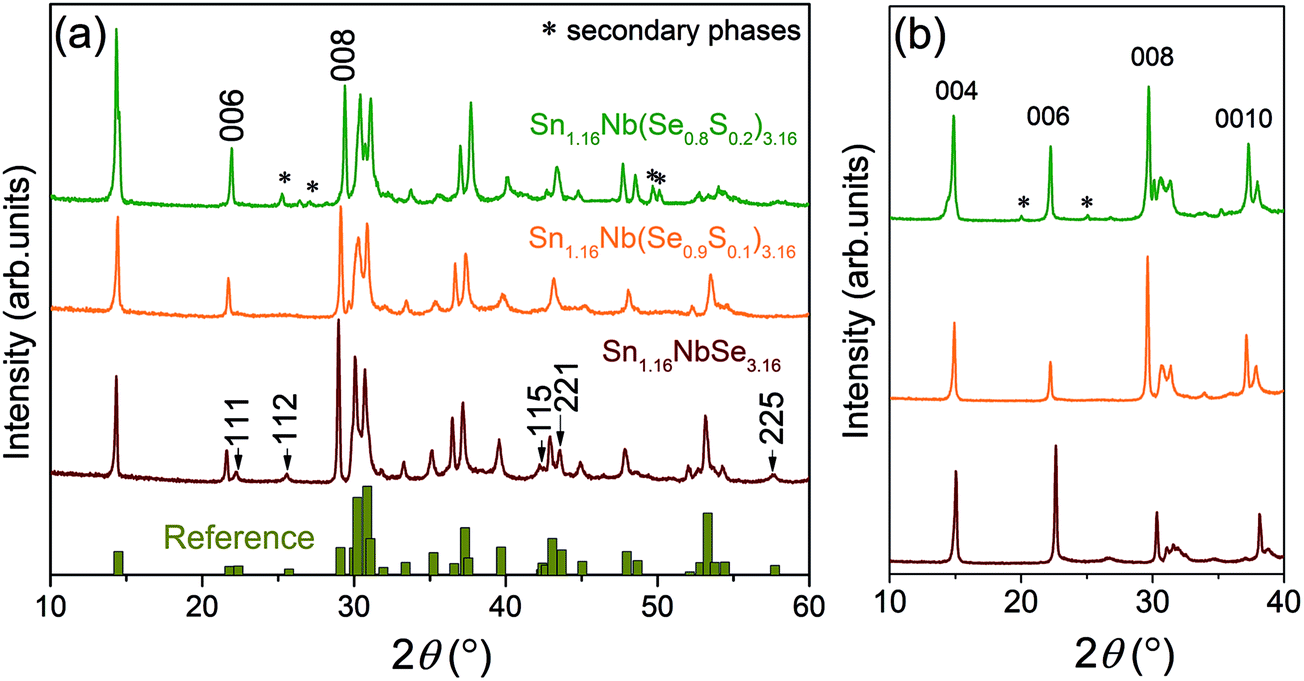 | ||
| Fig. 1 (a) Powder X-ray diffraction (XRD) patterns for Sn1.16Nb(Se1−xSx)3.16 (x = 0, 0.1, 0.2) along with the reference pattern.27 (b) Out-of-plane XRD patterns for Sn1.16Nb(Se1−xSx)3.16 (x = 0, 0.1, 0.2) sintered compacts. | ||
Table 1 shows the refined lattice parameters at room temperature for all the samples with typical refinement R values being, Rp ∼ 6.8% and Rwp ∼ 9.7%. The (SnSe)1.16NbSe2 system is indexed as CF type, where SnSe and NbSe2 layers have C and F centered orthorhombic lattices, respectively.27 Since this system is isostructural with (LaS)1.14NbS2, a similar approach of lattice refinement was followed using a (3 + 1)-dimensional superspace group Fm2m(p00)00s.34 Both layers have common b and c-axis, but incommensurate a-axis with the ratio of p = aNbSe2/aSnSe, considering (Sn2Se2)pNbSe2. With the substitution of Se for S, all the lattice parameters decrease considerably with ∼3–4% reduction in case of x = 0.1 to as high as ∼12–13% for x = 0.2 for both the layers, when compared with the pristine Se sample. This indicates that S might be occupying Se sites in both the layers. The reduction in lattice parameters is expected since S2− (1.84 Å for 6 coordination) has a smaller ionic radius than Se2− (1.98 Å for 6 coordination), and the presence of impurities (in x = 0.2 sample) and deviation from the ideal configuration is bound to cause some kind of crystallographic strains on the lattice. The lattice parameters can also be affected by the changes in charge transfer between SnSe and NbSe2 layers, which will be studied in the later section.
| Sample | Subgroup | a (Å) | b (Å) | c (Å) |
|---|---|---|---|---|
| Sn1.16NbSe3.16 | SnSe | 6.1 | 6.1 | 12.7 |
| NbSe2 | 3.6 | 6.1 | 25.3 | |
| Sn1.16Nb(Se0.9S0.1)3.16 | SnSe | 5.9 | 5.9 | 12.2 |
| NbSe2 | 3.4 | 5.9 | 24.4 | |
| Sn1.16Nb(Se0.8S0.2)3.16 | SnSe | 5.3 | 5.4 | 11.0 |
| NbSe2 | 3.1 | 5.4 | 22.1 |
Fig. 1b shows the XRD patterns for the surfaces perpendicular (out-of-plane) to the pressing directions for all the sintered compacts. All the samples show a strong normalized orientation index of the (00l) plane, indicating that the crystalline c-axis is preferably oriented along the out-of-plane direction, as reported for other misfit layered systems.20,25 The covalent bonding within the layers being much stronger than the interlayer bonding, causes the grains to grow in direction perpendicular to the pressure applied during sintering which gives the highly preferred (00l) orientation. The extent of grain orientation was analyzed using the peak intensity ratio ∑I(00l)/∑I(hkl). The pristine Se system showed the highest peak intensity ratio of 80% suggesting a highly oriented texture, followed by x = 0.1 with 73% and x = 0.2 with 61% with the least degree of orientation.
The SEM images of the sintered compacts shown in Fig. 2 strongly support the XRD patterns in regards to orientation and layering of grains. The grains in Sn1.16NbSe3.16 vary in size from 10 μm to 100 μm and are self-arranged into a layered structure (Fig. 2a). Fig. 2b provides a closer look at these sheets of grains. This natural layering of the grains is due to the anisotropic nature of the atomic bonds in these materials, as mentioned before. Sulfur doping, however, disrupts this preferential grain growth most likely due to the expected compositional disorder/defects arising from the presence of mixed anions. Fig. 2c shows the SEM image of Sn1.16Nb(Se0.9S0.1)3.16 sample with grains ∼20–30 μm in size with a slight orientation perpendicular to the pressing direction. This sample has a homogenous grain size distribution but lacks the layered ordering of the micrograins. For Sn1.16Nb(Se0.8S0.2)3.16, no grain orientation is apparent in the SEM image, (Fig. 2d) and the grain size distribution also appears to be very inhomogeneous most probably due to the secondary phase impurities present in this sample. Even the slightest compositional changes in these misfit layered systems can greatly influence the grain growth, as studied comprehensively in our previous work on (LaS)1.14NbS2 system.24
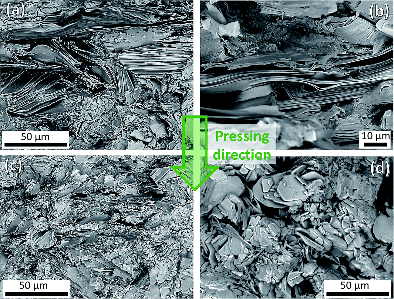 | ||
| Fig. 2 Scanning electron micrographs of the fractured areas of (a and b) Sn1.16NbSe3.16, (c) Sn1.16Nb(Se0.9S0.1)3.16 and (d) Sn1.16Nb(Se0.8S0.2)3.16 sintered compacts. | ||
3.2 Thermoelectric properties
The sintered density was confirmed to be higher than 95% of the theoretical density (6.32 g cm−3) for all the measured samples. Specifically, the density of Sn1.16NbSe3.16, Sn1.16Nb(Se0.9S0.1)3.16, and Sn1.16Nb(Se0.8S0.2)3.16 is 6.19 g cm−3, 6.11 g cm−3, and 6.01 g cm−3, respectively. From the room temperature Hall effect measurements and assuming parabolic bands and single-band conduction, we estimated the hole concentration (p) and carrier mobility (μ) using the relation: p = 1/eRH and μ = 1/peρ, where RH is the Hall coefficient and e represents electronic charge and ρ is electrical resistivity. Table 2 shows the RH, p and μ for all the samples. The sign of RH and Seebeck coefficient (S, Fig. 3b) are positive for all the samples indicating conduction by holes. This misfit selenide exhibits p-type metallic conduction in a more than half filled 4dz2 band, with a slight electron transfer from SnSe to NbSe2 layer.16,27 In (MS)1+m(TS2)n (M = Pb, Sn) misfits, the defects in the S lattice is proposed to be responsible for the slight charge (electron) transfer.16 A similar assumption can be made for our Se system as well, where the defects in the Se sites could be responsible for the slight charge transfer from the SnSe to the NbSe2 layer and the conduction only determined by holes in the dz2 band of NbSe2.| Sample | Direction | R H (109 m3 C−1) | p (1021 cm−3) | μ (cm2 V−1 s−1) | m*/m0 |
|---|---|---|---|---|---|
| Sn1.16NbSe3.16 | In-plane | 0.7 | 9.3 | 1.7 | 1.9 |
| Out-of-plane | 1.1 | 3.2 | |||
| Sn1.16Nb(Se0.9S0.1)3.16 | In-plane | 1.6 | 4.0 | 4.5 | 0.9 |
| Out-of-plane | 2.7 | 2.0 | |||
| Sn1.16Nb(Se0.8S0.2)3.16 | In-plane | 1.4 | 4.2 | 3.9 | 1.0 |
| Out-of-plane | 2.6 | 2.0 |
 | ||
| Fig. 3 Temperature dependencies of the (a) electrical resistivity (ρ), (b) Seebeck coefficient (S), and (c) power factor (S2/ρ) measured perpendicular (in-plane (ip)) and parallel (out-of-plane (op)) to the pressing direction for the Sn1.16Nb(Se1−xSx)3.16 (x = 0, 0.1, 0.2) sintered compacts. | ||
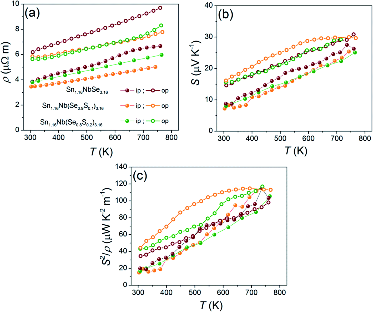
We measured RH ∼ 0.7 × 10⁻⁹ m3 C−1 and p ∼ 9.3 × 1021 cm−3 for pristine Se system, which is similar to the previously reported values (RH ∼ 0.6 × 10⁻⁹ m3 C−1 and p ∼ 9.6 × 1021 cm−3)27 at room temperature. This value of p corresponds to 1.3 holes/Nb atoms. With the substitution of Se for S, p reduces to less than half with a value of ∼4 × 1021 cm−3 corresponding to 0.5 holes/Nb atoms. The variation in holes/Nb atoms is known to be greatly affected by the extent of charge transfer with greater charge transfer leading to lower holes/Nb atoms.30 One assumption is that the substitution of Se for S increases the defects on the Se sites leading to excessive charge transfer from the SnSe layer to the NbSe2 layer, hence decreasing the holes/Nb atom in the NbSe2 layer. This assumption is also supported by the fact that μ of S doped samples is more than twice higher than the pristine Se system, even though the SEM images show better texturing of grains for the latter. For example, the in-plane and out-of-plane μ of (SnSe)1.16NbSe2 is 1.7 and 1.1 cm2 V−1 s−1, whereas for Sn1.16Nb(Se0.9S0.1)3.16 and Sn1.16Nb(Se0.8S0.2)3.16 the values are 4.5 and 2.7 cm2 V−1 s−1; 3.9 and 2.6 cm2 V−1 s−1, respectively. Higher charge transfer increases the strength of inter and intra layer bonding which can promote the better mobility of the charge carriers and also play a role in the decrease of the lattice parameters,32 which we also observe in Table 1.
The temperature dependence of electrical resistivity (ρ) and Seebeck coefficient (S) are shown in Fig. 3a and b, respectively. The samples exhibit a metallic behavior where ρ and S increase with temperature. As expected, the ρ of all the samples are highly anisotropic in accordance with the mobility (Table 2) trends. The oriented textures promote higher μ (1.7–4.5 cm2 V−1 s−1) and lower ρ (3.8–3.4 μΩ m) in the in-plane direction, while increased carrier scattering at the interfaces between the layers results in a lower μ (1.1–2.7 cm2 V−1 s−1) and ∼40% larger ρ (6.2–5.6 μΩ m) in the out-of-plane direction, for all the samples at room temperature. In general, the ρ of S containing samples is lower than the pristine Se system mainly due to higher carrier mobility in the former. The room temperature ρ values of our samples are similar to the ferecrystalline (SnSe)1.16NbSe2 (ref. 30) and its VSe2 variant,35 but is twice lower than its n-type TiSe2 variant (12–15 μΩ m).36
The Sn1.16Nb(Se0.9S0.1)3.16 sample shows the highest S almost over the entire temperature range owing to its lower p with a value of ∼16 μV K−1 at room temperature, peaking at 760 K to ∼30 μV K−1, followed by pristine (SnSe)1.16NbSe2 sample with ∼14 μV K−1 at room temperature and ∼31 μV K−1 at 760 K, in out-of-plane direction (Fig. 3b). These S values in general are much lower compared to the sulfide misfit systems (∼50–170 μV K−1 above 700 K)20,23 and do not lie in the range for good thermoelectric materials.
All the samples show anisotropic S in the whole temperature range measured; the in-plane S values are smaller (7–9 μV K−1) than the out-of-plane ones (14–16 μV K−1) (Fig. 3b). To analyze this anisotropy, we estimated the carrier (hole) effective mass m* from the measured n and S using the following relation.
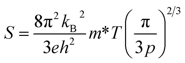 | (1) |
As shown in Fig. 3c, Sn1.16Nb(Se0.9S0.1)3.16 shows the highest power factor, S2/ρ, in out-of-plane direction in the entire temperature range with a value of ∼40 μW K−2 m−1 at 300 K and ∼120 μW K−2 m−1 at 760 K, which is about ∼15% improvement compared to the pristine Se system. The former has higher S2/ρ due to higher μ (low ρ) and lower p (high S), compared to the latter. In general, the S2/ρ values are higher in the out-of-plane directions than in the in-plane direction due to higher m* for all the samples in the out-of-plane direction. Although the introduction of S in Se site has proven beneficial in improving the S2/ρ of this system, the values are still much (2–3 times) lower compared with misfit layered sulfides reported in the past23 which is mostly due to a magnitude higher carrier concentration in our Se misfit system.
Fig. 4a and b shows the temperature dependences of the total thermal conductivity (κtotal) and lattice thermal conductivity (κlat) determined by subtracting electronic thermal conductivity (κel) from κtotal of Sn1.16Nb(Se1−xSx)3.16 (x = 0, 0.1, 0.2) in both the directions, respectively. The κel was estimated using the Wiedemann–Franz law given as κel = LT/ρ, where L is the Lorenz number (2.44 × 10⁻⁸ W Ω K−2). For all the samples in both directions, the κtotal and κlat are quite low and lie in the ranges from 3.0 to 5.4 W K−1 m−1 and 0.9 to 2.3 W K−1 m−1 at 760 K, respectively, with in-plane values being higher than the out-of-plane ones. This is because the interfaces between the layers effectively scatter the longer wavelength heat-carrying phonons, as is expected in layered systems. However, the κlat of these misfit selenides are slightly higher than for misfit sulfides (0.3–1.9 W K−1 m−1 at high temperatures),23 which adds to their disadvantage. For pristine Sn1.16NbSe3.16 sample, the difference between its in-plane (∼2.3 W K−1 m−1) and out-of-plane (∼1.0 W K−1 m−1) κlat is the largest with the former being twice larger at 760 K and is due to the increased interlayer and boundary scatterings arising from strong orientation of grains (as observed through SEM). S doping disrupts the strong grain orientation and also results in a smaller grain size, owing to which Sn1.16Nb(Se0.9S0.1)3.16 and Sn1.16Nb(Se0.8S0.2)3.16 have a much lower in-plane κlat (∼1.8 W K−1 m−1 and ∼1.1 W K−1 m−1, respectively). The additional impurities in Sn1.16Nb(Se0.8S0.2)3.16 must also contribute towards its low κlat.
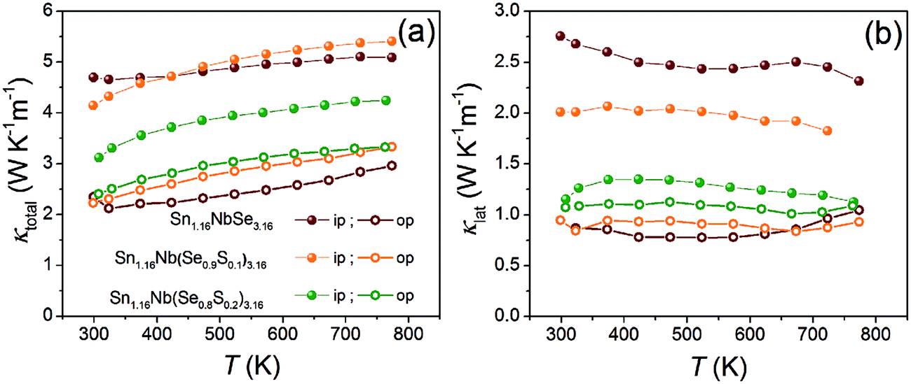 | ||
| Fig. 4 Temperature dependencies of (a) total thermal conductivity (κtotal), and (b) lattice thermal conductivity (κlat) measured perpendicular (in-plane (ip)) and parallel (out-of-plane (op)) to the pressing direction for the Sn1.16Nb(Se1−xSx)3.16 (x = 0, 0.1, 0.2) sintered compacts. | ||
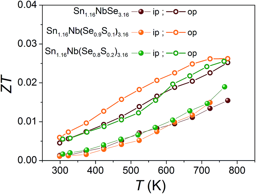
The thermoelectric figure of merit (ZT) for the misfit layered selenides, Sn1.16Nb(Se1−xSx)3.16 (x = 0, 0.1, 0.2), in the in-plane and out-of-plane directions calculated from the measured ρ, S, and κtotal are shown in Fig. 5. Sn1.16Nb(Se0.9S0.1)3.16 has the highest ZT in the whole temperature range with a value of ∼0.03 at 760 K, mainly due its higher S2/ρ compared to the other samples. These ZT values are very low for this selenide system to be considered as a potential thermoelectric material, mainly due to the high hole concentration in the system. In order to enhance ZT, further carrier concentration optimization needs to be performed on this system. One way, is to synthesize compound with paired NbSe2 layers (for example, (SnSe)1.16(NbSe2)n, n = 2, 3) to tune the charge transfer which could ultimately lead to lower p. Proper doping on anion or cation sites as well as studying the effects of non-stoichiometry can also be useful in enhancing the thermoelectric properties of this Se misfit system.
 | ||
| Fig. 5 Temperature dependence of the thermoelectric figure of merit (ZT) measured perpendicular (in-plane (ip)) and parallel (out-of-plane (op)) to the pressing direction for the Sn1.16Nb(Se1−xSx)3.16 (x = 0, 0.1, 0.2) sintered compacts. | ||
4. Conclusion
Here, we synthesized bulk polycrystalline misfit layered selenides Sn1.16Nb(Se1−xSx)3.16 (x = 0, 0.1, 0.2) and studied their temperature dependent thermoelectric properties for the first time. S doping was performed to improve the thermoelectric properties of the system. S doping seemed to increase the charge transfer from the SnSe to NbSe2 layers, thereby reducing the hole concentration and increasing the hole mobility in the system. This resulted in slightly higher S and lower ρ, owing to which 15% higher S2/ρ ∼ 120 μW K−2 m−1 at 760 K was achieved for S doped system compared to the pristine Se system, in out-of-plane direction. For all the samples, the κlat is quite low and lie in the ranges from 0.9 to 2.3 W K−1 m−1 in the out-of-plane direction at 760 K. Despite such low κlat, this Se misfit shows poor maximum ZT (∼0.03 at 760 K) due to its low S2/ρ arising from high hole concentration. Further carrier concentration optimizations need to be performed on this system through relevant dopings or making compound with paired NbSe2 layers. At the same time, other Se misfit compounds should be explored, such as TiSe2, VSe2, CrSe2, TaSe2 host layer compounds and rare-earth intercalation compounds, in order to determine the true potential of layered Se misfits for thermoelectrics.Author contributions
P. J. and M. O. designed the experiments. P. J. prepared the powders and sintered samples and performed the XRD experiments and measured the electrical and thermal transport properties. Both authors discussed the results and contributed to writing of the manuscript.Conflict of interest
The authors have declared no conflicts of interest.Acknowledgements
The authors express our thanks to Ms Naoko Fujimoto of AIST for measuring the electrical and thermal transport properties. The work was supported by Bilateral Joint Research Projects between the Japan Society for the Promotion of Science and French Ministry of Foreign Affairs and International Development (JSPS-MAEDI SAKURA Program).References
- G. A. Slack, CRC Handbook of Thermoelectrics, CRC Press, Boca Raton, FL, 1995 Search PubMed.
- B. C. Sales, D. Mandrus and R. K. Williams, Science, 1996, 272, 1325–1328 CAS.
- G. S. Nolas, J. L. Cohn, G. A. Slack and S. B. Schujman, Appl. Phys. Lett., 1998, 73, 178–180 CrossRef CAS.
- K. Suekuni, K. Tsuruta, M. Kunii, H. Nishiate, E. Nishibori, S. Maki, M. Ohta, A. Yamamoto and M. Koyano, J. Appl. Phys., 2013, 113, 043712 CrossRef.
- M. G. Kanatzidis, Chem. Mater., 2010, 22, 648–659 CrossRef CAS.
- M. Ohta, K. Biswas, S.-H. Lo, J. He, D. Y. Chung, V. P. Dravid and M. G. Kanatzidis, Adv. Energy Mater., 2012, 2, 1038 CrossRef.
- P. Jood, R. J. Mehta, Y. Zhang, G. Peleckis, X. Wang, R. W. Siegel, T. Borca-Tasciuc, S. X. Dou and G. Ramanath, Nano Lett., 2011, 11, 4337–4342 CrossRef CAS PubMed.
- C. Chiritescu, D. G. Cahill, N. Nguyen, D. Johnson, A. Bodapati, P. Keblinski and P. Zschack, Science, 2007, 315, 351–353 CrossRef CAS PubMed.
- I. Terasaki, Y. Sasago and K. Uchinokura, Phys. Rev. B: Condens. Matter Mater. Phys., 1997, 56, R12685–R12687 CrossRef CAS.
- K. Koumoto, I. Terasaki and R. Funahashi, MRS Bull., 2006, 31, 206–210 CrossRef CAS.
- R. Funahashi, I. Matsubara, H. Ikuta, T. Takeuchi, U. Mizutani and S. Sodeoka, Jpn. J. Appl. Phys., Part 1, 2000, 39, L1127–L1129 CAS.
- M. Ohta, S. Satoh, T. Kuzuya, S. Hirai, M. Kunii and A. Yamamoto, Acta Mater., 2012, 60, 7232–7240 CrossRef CAS.
- M. Ohta, D. Y. Chung, M. Kunii and M. G. Kanatzidis, J. Mater. Chem. A, 2014, 2, 20048–20058 CAS.
- M. Lee, L. Viciu, L. Li, Y. Wang, M. L. Foo, S. Watauchi, R. A. Pascal Jr, R. J. Cava and N. P. Ong, Nat. Mater., 2006, 5, 537–540 CrossRef CAS PubMed.
- S. Hébert, W. Kobayashi, H. Muguerra, Y. Bréard, N. Raghavendra, F. Gascoin, E. Guilmeau and A. Maignan, Phys. Status Solidi, 2013, 210, 69–81 CrossRef.
- G. A. Wiegers, Prog. Solid State Chem., 1997, 24, 1–139 CrossRef.
- C. M. Fang, S. v. Smaalen, G. A. Wiegers, C. Haas and R. A. d. Gsroot, J. Phys.: Condens. Matter, 1996, 8, 5367–5382 CrossRef CAS.
- S. H. Han and B. A. Cook, AIP Conf. Proc., 1994, 316, 66–70 CrossRef.
- H. Imai, Y. Shimakawa and Y. Kubo, Phys. Rev. B: Condens. Matter Mater. Phys., 2001, 64, 241104(R) CrossRef.
- C. Wan, Y. Wang, N. Wang and K. Koumoto, Materials, 2010, 3, 2606–2617 CrossRef CAS.
- E. Guilmeau, Y. Bréard and A. Maignan, Appl. Phys. Lett., 2011, 99, 052107 CrossRef.
- C. Wan, Y. Wang, W. Norimatsu, M. Kusunoki and K. Koumoto, Appl. Phys. Lett., 2012, 100, 101913 CrossRef.
- P. Jood and M. Ohta, Materials, 2015, 8, 1124–1149 CrossRef.
- P. Jood, M. Ohta, O. I. Lebedev and D. Berthebaud, Chem. Mater., 2015, 27, 7719–7728 CrossRef CAS.
- P. Jood, M. Ohta, H. Nishiate, A. Yamamoto, O. I. Lebedev, D. Berthebaud, K. Suekuni and M. Kunii, Chem. Mater., 2014, 26, 2684–2692 CrossRef CAS.
- C. Wan, X. Gu, F. Dang, T. Itoh, Y. Wang, H. Sasaki, M. Kondo, K. Koga, K. Yabuki, G. J. Snyder, R. Yang and K. Koumoto, Nat. Mater., 2015, 14, 622–627 CrossRef CAS PubMed.
- G. A. Wiegers and W. Y. Zhou, Mater. Res. Bull., 1991, 26, 879–885 CrossRef CAS.
- R. D. Westover, R. A. Atkins, J. J. Ditto and D. C. Johnson, Chem. Mater., 2014, 26, 3443–3449 CrossRef CAS.
- M. B. Alemayehu, M. Falmbigl, C. Grosse, K. Ta, S. F. Fischer and D. C. Johnson, J. Alloys Compd., 2015, 619, 861–868 CrossRef CAS.
- M. B. Alemayehu, M. Falmbigl, K. Ta, C. Grosse, R. D. Westover, S. R. Bauers, S. F. Fischer and D. C. Johnson, Chem. Mater., 2015, 27, 867–875 CrossRef CAS.
- F. Gascoin, N. Raghavendra, E. Guilmeau and Y. Bréard, J. Alloys Compd., 2012, 521, 121–125 CrossRef CAS.
- K. Kisoda, M. Hangyo, J. Kuroda, H. Harima and S. Nakashima, Solid State Commun., 1997, 103, 597–602 CrossRef CAS.
- V. Petříček, M. Dusek, and L. Palatinus, Jana2006, the crystallographic computing system, Czech Republic: Institute of Physics, Praha, 2006 Search PubMed.
- Y. Miyazaki, H. Ogawa, T. Nakajo, Y. Kikuchii and K. Hayashi, J. Electron. Mater., 2013, 42, 1335–1339 CrossRef CAS.
- R. Atkins, S. Disch, Z. Jones, I. Haeusler, C. Grosse, S. F. Fischer, W. Neumann, P. Zschack and D. C. Johnson, J. Solid State Chem., 2013, 202, 128–133 CrossRef CAS.
- D. R. Merrill, D. B. Moore, J. Ditto, D. R. Sutherland, M. Falmbigl, M. Winkler, H. F. Pernau and D. C. Johnson, Eur. J. Inorg. Chem., 2015, 83–91 CrossRef CAS.
- C. Wan, Y. Wang, N. Wang, W. Norimatsu, M. Kusunoki and K. Koumoto, J. Electron. Mater., 2011, 40, 1271–1280 CrossRef CAS.
| This journal is © The Royal Society of Chemistry 2016 |