DOI:
10.1039/C6RA20338H
(Paper)
RSC Adv., 2016,
6, 91370-91376
Controlled synthesis of nanotubes and nanowires decorated with TiO2 nanocuboids with exposed highly reactive (111) facets to produce enhanced photoelectrochemical properties†
Received
12th August 2016
, Accepted 9th September 2016
First published on 9th September 2016
Abstract
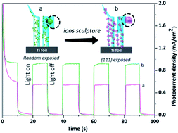
The ability to control the exposure of facets of a crystal has been garnering considerable attention due to the fascinating dependence of the physical properties of crystals on their shapes. Herein, a TiO2WT photoelectrode decorated with anatase TiO2 nanocuboids (TiO2C111WTs) displaying high-energy exposed (111) facets and quantum dot dimensions was prepared for the first time by using a TiCl4 treatment process. F− and NH4+ were introduced together to limit the randomness of the TiCl4 hydrolysates. We propose that both F− and NH4+ were necessary for controlling the exposure of the (111) facets. In comparison with TiO2WT photoelectrodes decorated with either randomly deposited TiO2 nanoparticles (non-facet) or with TiO2 nanofilms or with TiO2 nanocuboids displaying exposed {001} facets (denoted as TiO2PWT, TiO2FWT and TiO2C001WT photoelectrodes, respectively), the hybrid-structured TiO2C111WT photoelectrode achieved superior PEC performances, with Jsc and photoconversion efficiency values of 0.97 mA cm−2 and 0.49%. This enhancement was attributed to the exposure of the highly active (111) facets and the increased specific surface area of TiO2C111WTs. Meanwhile, the photoactive (111) facets offered oxygen vacancies, resulting in an increase of donor density and the enhancement of PEC performances. These facets also promoted the adsorption of CdS QDs and hence further sensitization. The CdS/TiO2C111WTs achieved Jsc and photoconversion efficiency values of 3.95 mA cm−2 and 2.05%, which were about twice those of CdS/TiO2WTs.
1. Introduction
Anatase titanium dioxide (TiO2) photoelectrodes constitute one of the most important semiconductors, playing an important role in solar energy conversion applications, and tremendous attention has been paid to improving its photoelectrochemical (PEC) properties.1–10 One-dimensional nanostructured TiO2 forms, such as nanowires and nanotubes, have been considered as candidates with enhanced efficiencies due to their direct pathways, which facilitate electron transport.11,12 Moreover, these morphologies display large surface-to-volume ratios, and such morphologies can thus load more quantum dots (QDs) and provide more effective contact areas with the electrolyte.13 Thus, the hybrid structure of nanowire-decorated nanotubes (denoted here as TiO2WTs) combines the advantages of both the nanotube and nanowire in charge separation, electron transport and light harvesting,14–16 which broaden its prospects for many solar energy conversion applications.17
In recent years, considerable efforts have been devoted to improving the PEC properties of TiO2 photoelectrodes.14,18,19 TiCl4 treatment is a simple and effective method,20,21 which could decorate the structure with an extra layer of TiO2 nanoparticles. These nanoparticles effectively enhance PEC performance by increasing the contact areas of TiO2 photoelectrodes with electrolyte and reducing the recombination rate at the TiO2/electrolyte interface by passivating the surface defects.22 However, those nanoparticles were found to be attached to TiO2WTs in random orientations (non-facet), which restricts the further improvement of its PEC properties.
PEC properties differ for different TiO2 facets, which has been attributed to their different bandgaps and surface electronic band structures.23,24 The use of uniformly exposed high-energy facets of TiO2 crystals could provide an approach for achieving a superior PEC performance,25–27 by improving the utilization rate of the surface. Theoretical results have indicated the order of the average surface energies of anatase TiO2 to be {111} facets (1.61 J m−2) > {001} facets (0.90 J m−2) > {010} facets (0.53 J m−2) > {101} facets (0.44 J m−2).28–31 Moreover, the {111} facet, much of which is formed by undercoordinated Ti (Ti5c and Ti3c) atoms and O (O2c) atoms (as shown in Fig. S1 in ESI†). These undercoordinated atoms affect the electronic properties by forming oxygen vacancies (donor densities) and hence acting as active sites in the photoreaction.28,32,33 Consequently, the {111} facets of anatase TiO2 have been considered as the most active facets in solar applications. Nevertheless, the energy values of facets with initially high surface energies diminish rapidly during the crystal growth process to minimize the total crystal energy.34 Hence, it is important to explore an efficient method to accurately control the exposure of the {111} facets of TiO2 nanoparticles that attach to TiO2WTs.
In the present work, we successfully controlled the uniform exposed facets of TiO2 nanoparticles attached to TiO2WTs, by introducing F−/NH4+ ions during the TiCl4 treatment process. We synthesized TiO2WTs photoelectrodes with randomly deposited TiO2 nanoparticles (non-facet), TiO2 nanofilms, TiO2 nanocuboids with exposed {001} facets, and TiO2 nanocuboids with exposed (111) facets, denoted as TiO2 PWTs, TiO2 FWTs, TiO2C001WTs and TiO2C111WTs, respectively, as illustrated in Scheme 1. Then we demonstrated that the TiO2C111WT photoelectrode displayed significantly greater PEC performances than did the other TiO2WT photoelectrodes, owing to its increased surface-to-volume ratio and highly reactive (111) exposed facets, which effectively increased the utilization rate of the photoelectrode surface. Afterwards, we deposited CdS QDs on the photoelectrodes using the successive ionic layer adsorption and reaction (SILAR) method. The CdS/TiO2C111WT photoelectrode presents superior PEC performance, owing to the exposed high-energy (111) facets, which are the predominant sources of active sites and which favor CdS adsorption. This photoelectrode could be an excellent candidate for use in photovoltaics, gas sensors, photo-catalysis, Li-ion batteries and water splitting.
 |
| | Scheme 1 Schematic illustration of the primary TiCl4 treatment process from which TiO2 PWTs were obtained (A). Introducing F−/NH4+ ions during the TiCl4 treatment process resulted in TiO2 FWTs, TiO2C001WTs and TiO2C111WTs being obtained (B). | |
2. Experimental
2.1 Synthesis
All chemicals used were of the highest purity available and used as received without further purification. Deionized water was used in all cases. The TiO2WT photoelectrode was prepared by carrying out an electrochemical anodization of a Ti foil as in our previous work (with details described in ESI†).14
To prepare the TiO2C111WT photoelectrode, a TiO2WT photoelectrode was immersed into an aqueous solution containing 25 mM TiCl4 and 2.6 mM (NH4)2TiF6 at 70 °C for 20 min. Then, the treated photoelectrode was washed with DI water and annealed in the air at 450 °C for 1 h. In order to obtain a fair comparison, before characterization, the original TiO2WT photoelectrode was annealed for a second time at 450 °C in air for 1 h.
The procedures used to prepare the TiO2 PWT, TiO2 FWT, and TiO2C001WT photoelectrodes were similar to the preparation process described above, the only difference was the addition amount of F− and NH4+ ions in solution containing TiCl4. The details of these procedures are shown in ESI.†
2.1.1 Preparation of CdS QD-sensitized TiO2 photoelectrodes. CdS QDs were assembled onto photoelectrodes by using the SILAR technique. Specifically, as-prepared TiO2 photoelectrodes were successively immersed into three different solutions for 10 min each: first in 1 M mercaptoacetic acid in ethanol, then in 0.5 M Cd(NO3)2·4H2O in ethanol, and then in 0.5 M Na2S in deionized water. Following each immersion, the photoelectrodes were respectively rinsed with pure ethanol and deionized water to remove excess precursors and dried in air before the next dipping. This process was repeated six times. Eventually, the samples were annealed at 300 °C for 1 h.
2.2 Characterization of the materials
Scanning electron microscopy (SEM) images and EDS patterns were acquired by using a field-emission SEM (JEOL JSM-6700F). Transmission electron microscope (TEM) and high-resolution TEM (HR-TEM) images were acquired with a JEM-2100F high-resolution transmission microscope operating at 200 kV. X-ray diffraction (XRD) spectra of samples were obtained with a Rigaku D/max-2500 X-ray diffractometer with Cu Kα radiation (λ = 1.5418 Å). Raman spectra were acquired by using a Renishaw spectrometer (Renishaw in Via) equipped with a microscope (50× objective) with a spot size of 5–10 μm. Optical characterization (UV-Vis absorption spectroscopy) of the films was performed using a UV-3150 double-beam spectro-photometer (Shimadzu UV-3150).
2.3 Determination of photoelectrochemical (PEC) properties
The PEC properties of TiO2 and CdS/TiO2 photoelectrodes were determined by using a three-electrode electrochemical system made of a quartz cell and linked with an electrochemical workstation (CH Instruments, model CHI601C), and using an SCE reference electrode, a Pt wire as the counter electrode, and a 500 W Xe lamp (Spectra Physics) with a monochromator for simulated sunlight. Before the tests, a laser power meter (BG26M92C, Midwest Group) was used to adjust the light intensity, as effective as AM 1.5 light at 100 mW cm−2. A mask with a 0.25 cm2 window was clipped on the TiO2 side to define the working area. The electrolyte solution was an aqueous solution composed of 0.25 M Na2S·9H2O, 0.35 M Na2SO3 and 0.1 M KCl (pH = 12). Transient photocurrent response (I–T) measurements were taken at a potential of 0 V versus SCE. Mott–Schottky plots were collected at a frequency of 5 kHz in a three-electrode electrochemical system made of a quartz cell and linked with an electrochemical workstation (CH Instruments, model CHI660E), and using an Ag/AgCl reference electrode and a Pt wire as the counter electrode.
3. Results and discussion
3.1 Morphological characterization of the TiO2 photoelectrodes
SEM and TEM images of as-prepared TiO2PWTs, TiO2FWTs, TiO2C001WTs, and TiO2C111WTs are shown in Fig. 1. After TiCl4 treatment, TiO2WTs were decorated with TiO2 nanoparticles/film (Fig. 1A, D, G and J), and they retained the original morphology (WT hybrid structure), as shown in Fig. S3.†
 |
| | Fig. 1 SEM and TEM images of TiO2 PWTs (A–C), TiO2 FWTs (D–F), TiO2C001WTs (G–I) and TiO2C111WTs (J–L). | |
For the TiO2PWT photoelectrode, nanoparticles attached to the TiO2 tubes were randomly shaped (Fig. 1B). The HR-TEM result (Fig. 1C) further indicated that the outer-layer crystallites next to the exposed facets of the TiO2 tube were also random (non-facet). As shown in Fig. 1C, the corresponding lattice fringes were found to be d{004} = 0.237 nm and d{103} = 0.244 nm, which could be indexed to the anatase phase of TiO2 [JCPDS no. 71-1166]. When only introducing NH4+ ions, as shown in Fig. 1E, the nanoparticles ultimately merged into the film (14 nm), and the HR-TEM results (Fig. 1F) showed a d{204} crystalline spacing of 0.148 nm, corresponding to the anatase phase of TiO2. When only introducing F− ions, as shown in Fig. 1H, the nanoparticles adopted nanocuboid shapes (with dimensions of 12 nm). Their exposed facets were {001}, as indicated by the HR-TEM results in Fig. 1I, which also showed a lattice spacing of 0.189 nm for both d{020} and d{200}, which were observed to be related by an angle of 90°, indicating that the {001} facets constituted the basal plane of the cuboid, perpendicular to the [001] direction. The Fast-Fourier Transform (FFT) pattern (insert of Fig. 1I) provided further evidence that the {001} facets were the exposed facets. When introducing both NH4+ and F− ions, cuboid-shaped nanoparticles with dimensions of 12 nm were observed in their SEM image (Fig. 1K), and the corresponding HR-TEM image (Fig. 1L) showed lattice spacings of 0.352 nm and 0.350 nm related by an angle of 82° and matching the spacings between the {101} and {011} planes of anatase TiO2 with the [111] zone axis. These observations confirmed the top and bottom faces of the nanocuboid to be the high-energy {111} facets.
In addition, we could see that the nanoparticle, nanofilm and nanocuboid lattices were stacked on the nanotube lattices with a certain angle at their interface, revealing that all of the nanoparticles and nanocuboids as well as the nanofilm grew on the nanotube. The interfaces between nanocuboids and nanotubes resulted in more charge transfer channels, which could enhance the injection of electrons.
We noticed that the inclusion of both F− and NH4+ was necessary to control the exposure of the {111} facets, and similar results were shown in the investigations by Sinha et al.35 They pointed out that the formation of ammonium titanium oxide fluoride (NH4)2(TiF4O) was important for leaving, the TiO2 crystals with exposed {111} facets after the annealing process. When only NH4+ was introduced into the system, the boundaries between nanoparticles vanished. Although we were not able to observe the exact process by which the nanoparticles aggregated, we would like to propose that NH4+ accelerated the deposition of TiO2 nanoparticles. When only F− was introduced in the system, F− selectively adsorbed on {001} facets to reduce the surface energy during the TiCl4 hydrolyzation process, and then left TiO2 with exposed {001} facets.36
3.2 Performances of the TiO2 PWT, TiO2 FWT, TiO2C001WT, and TiO2C111WT photoelectrodes
Fig. 2A shows XRD patterns for the TiO2 WT, TiO2 PWT, TiO2 FWT, TiO2C001WT, and TiO2C111WT photoelectrodes. All of the diffraction peaks in these patterns were found to correspond to anatase TiO2 [JCPDS no. 71-1166] and Ti base, indicating that these TiO2 WT photoelectrodes were pure anatase TiO2. The strongest diffraction peak centered at 2-theta of 25° was attributed to the crystal face {101}. These results were also indicated by the corresponding Raman spectra (Fig. 2B). For the original and treated TiO2WT photoelectrodes, five major Raman bands were observed at frequencies of 144, 196, 395, 516, and 637 cm−1, which were assigned as Eg(1), Eg(2), B1g(1), B1g(2) + A1g and Eg(3) vibration modes of anatase TiO2, respectively.37
 |
| | Fig. 2 XRD patterns (A) and Raman spectra (B) for the TiO2 WT, TiO2 PWT, TiO2 FWT, TiO2C001WT, and TiO2C111WT photoelectrodes. | |
Fig. 3A shows the UV-Vis absorption spectra of the photoelectrodes. These samples absorbed mainly UV light with wavelengths of about 370–385 nm, corresponding to 3.2–3.3 eV band gaps, and no significant absorbance was observed in the visible region. The TiO2C111WT photoelectrode showed the strongest absorbance, with the order of the absorbance intensities being TiO2C111WTs > TiO2C001WTs > TiO2FWTs > TiO2PWTs > TiO2WTs. The superior absorbance of the TiO2C111WT photoelectrode than other photoelectrodes could be attributed to the exposure of highly active facets. Moreover, the {111} facets may have many oxygen vacancies, which would have improved the light utilization, and thus enhanced the absorbance intensity.
 |
| | Fig. 3 UV-Vis absorption spectra (A), J–V curves (B), photoconversion efficiencies (C) and I–T measurements (D) of TiO2WT, TiO2PWT, TiO2FWT, TiO2C001WT, and TiO2C111WT photoelectrodes. | |
The PEC performances of the various photoelectrode samples were evaluated by measuring their photocurrent densities under simulated sun light illumination (100 mW cm−2, AM 1.5 G). Fig. 3B and C show linear sweep voltammetry (J–V) curves and chemical energy conversion (photoconversion) efficiencies recorded from these photoelectrodes. The TiO2C111WT photoelectrode achieved a short-circuit current density (Jsc) and photoconversion efficiency of 0.97 mA cm−2 and 0.49%, respectively, which were much higher than those of the other electrodes, i.e., the TiO2C001WT (0.76 mA cm−2 and 0.46%), TiO2FWT (0.66 mA cm−2 and 0.41%), TiO2PWT (0.56 mA cm−2 and 0.36%), and TiO2WT (0.52 mA cm−2 and 0.31%) photoelectrodes. The results indicated that the energy conversion efficiency of the photoelectrode increased sharply when modified with QD-sized TiO2 nanocuboids with exposed (111) facets. Fig. 3D shows the transient photocurrent response (I–T) measurement of the aforementioned photoelectrodes. All of the photoelectrodes showed relatively good reproducibility and stability when illumination was turned on and off. The observed dark current densities (light off) for all photoelectrodes were negligible. A remarkable enhancement of the photocurrent response performance of the TiO2C111WT photoelectrode was observed, which could be attributed to the exposure of the highly active (111) facets. These facets increased the contact areas of the photoelectrode with electrolyte. Meanwhile, the photoactive (111) facets may have increased the number of oxygen vacancies, resulting in an increase of donor density. Furthermore, empirical evidence of such an increase was given by Mott–Schottky plots (Fig. S5†). The charge carrier density of the TiO2C111WTs was calculated to be 1.042 × 1021 cm−3, larger than the 0.431 × 1021 cm−3 value for TiO2WTs.
3.3 PEC performances of CdS-sensitized TiO2 WT, TiO2 PWT, TiO2 FWT, TiO2C001WT, and TiO2C111WT photoelectrodes
In order to broaden the photoresponses of these samples to the visible light region, we sensitized the TiO2 photoelectrodes with CdS QDs and evaluated their PEC performances. Fig. 4A and B show the J–V curves and photoconversion efficiencies of TiO2WT, TiO2PWT, TiO2FWT, TiO2C001WT, and TiO2C111WT photoelectrodes sensitized with CdS QDs. The CdS/TiO2C111WT photoelectrode exhibited Jsc and photoconversion efficiency values (3.95 mA cm−2 and 2.05%) superior to those of the CdS/TiO2C001WT (2.74 mA cm−2 and 1.72%), CdS/TiO2FWT (2.47 mA cm−2 and 1.68%), CdS/TiO2PWT (2.08 mA cm−2 and 1.66%) and CdS/TiO2WT (1.49 mA cm−2 and 1.17%) photoelectrodes. The superior photoconversion efficiency of the CdS/TiO2C111WT photoelectrode was attributed to the contribution of the highly active exposed (111) facets and oxygen vacancies of the TiO2C111WTs, which would allow more CdS QDs to be loaded on the TiO2C111WTs surface and hence produce more photoelectrons. This hypothesis was supported by the ICP-AES results shown in Table 1 in ESI:† the amount of CdS per unit area was calculated to be greater for the CdS/TiO2C111WTs than for the others. Moreover, the increased surface area would also contribute to the enhancement of the PEC performance by providing more electrochemical reaction locations at the interface between CdS/TiO2C111WTs and the electrolyte.
 |
| | Fig. 4 J–V curves (A) and photoconversion efficiencies (B) of CdS-sensitized TiO2 WT, TiO2 PWT, TiO2 FWT, TiO2C001WT, and TiO2C111WT photoelectrodes. | |
4. Conclusions
In summary, this paper reports an effective way to obtain (111)-facet-exposed quantum-dot-sized TiO2 nanocuboids. These nanocuboids were then attached to the surfaces of TiO2WT photoelectrodes. We propose that both F− and NH4+ together played important roles in exposing the (111) facets. This hybrid-structured TiO2C111WT photoelectrode exhibited improved surfactivity and superior PEC performances. The TiO2C111WT photoelectrode achieved Jsc and photoconversion efficiency values of 0.97 mA cm−2 and 0.49%, much higher than those achieved by the other photoelectrodes tested. This considerably enhanced PEC performance of the TiO2C111WT photoelectrode can be attributed to its larger surface-to-volume ratio — and to this photoelectrode simultaneously having exposed highly reactive (111) facets and oxygen vacancies, which in turn was due to its superior surface atomic structure with a large percentage of undercoordinated atoms for (111) facets. Furthermore, we broadened the photoresponse regions of these samples in the visible light range by sensitizing the TiO2 photoelectrodes with CdS QDs. The CdS/TiO2C111WT photoelectrode showed PEC performances, specifically Jsc and maximum photoconversion efficiency values of 3.95 mA cm−2 and 2.05%, respectively, that were better than those of the other hybrid-structured photoelectrodes. This enhancement was attributed to the TiO2C111WT photoelectrode being able to adsorb many CdS QDs owing to the exposed highly active (111) facets. The exposure of these facets was confirmed by EDS, UV-Vis absorption spectra, XRD, Raman and ICP-AES results.
Importantly, this method, which helped control the exposure of facets of nanocuboids in TiO2WT hybrid-structured photoelectrodes, could be further applied to other TiO2 photoelectrode shapes such as nanorods and nanofilms. Moreover, the ability to improve the surface utilization rate of the TiO2 photoelectrode opens up new opportunities in various areas, including PEC water splitting, dye-sensitized solar cells and photocatalysis. By replacing the original TiO2 with hybrid-structured ones, the efficiencies of their devices are expected to be enhanced.
Acknowledgements
This work was financially supported by the Technology Development Program of Jilin Province (Grant no. 20130206078GX).
Notes and references
- F. F. Cao, X. L. Wu, S. Xin, Y. G. Guo and L. J. Wan, Facile Synthesis of Mesoporous TiO2-C Nanosphere as an Improved Anode Material for Superior High Rate 1.5 V Rechargeable Li Ion Batteries Containing LiFePO4-C Cathode, J. Phys. Chem. C, 2010, 114, 10308–10313 CAS.
- Y.-K. Kim and D.-H. Min, UV Protection of Reduced Graphene Oxide Films by TiO2 Nanoparticle Incorporation, Nanoscale, 2013, 5, 3638–3642 RSC.
- S. Wang, L. Zhao, L. N. Bai, J. N. Yan, Q. Jiang and J. S. Lian, Enhancing Photocatalytic Activity of Disorder-engineered C/TiO2 and TiO2 Nanoparticles, J. Mater. Chem. A, 2014, 2, 7439–7445 CAS.
- O. Guaitella, C. Lazzaroni, D. Marinov and A. Rousseau, Evidence of Atomic Adsorption on TiO2 Under Plasma Exposure and Related C2H2 Surface Reactivity, Appl. Phys. Lett., 2010, 97, 011502 CrossRef.
- F. Sauvage, F. D. Fonzo, A. L. Bassi, V. Casari, G. Russo, C. Divitini, C. E. Bottani, P. Comte and M. Hierarchical, TiO2 Photoanode for Dye-Sensitized Solar Cells, Nano Lett., 2010, 10, 2562–2567 CrossRef CAS PubMed.
- A. Salant, M. Shalom, I. Hod, A. Faust, A. Zaban and U. Banin, Quantum Dot Sensitized Solar Cells with Improved Efficiency Prepared Using Electrophoretic Deposition, ACS Nano, 2010, 10, 5962–5968 CrossRef PubMed.
- Z. H. Zhang, L. B. Zhang, H. Mohamed Nejib, H. N. Zhang and P. Wang, Plasmonic Gold Nanocrystals Coupled with Photonic Crystal Seamlessly on TiO2 Nanotube Photoelectrodes for Efficient Visible Light Photoelectrochemical Water Splitting, Nano Lett., 2013, 13(1), 14–20 CrossRef CAS PubMed.
- J. Park, S. Bauer, K. von der Mark and P. Schmuki, Nanosize and Vitality: TiO2 Nanotube Diameter Directs Cell Fate, Nano Lett., 2007, 7(6), 1686–1691 CrossRef CAS PubMed.
- H. A. Hamedani, J. A. Khaleel, K. H. Dahmen and H. Garmestani, Surface Controlled Growth of Thin-Film Strontium Titanate Nanotube Arrays on Silicon, Cryst. Growth Des., 2014, 14, 4911–4919 Search PubMed.
- C. Adán, J. Marugán, E. Sánchez, C. Pablos and R. V. Grieken, Understanding the Effect of Morphology on the Photocatalytic Activity of TiO2 Nanotube Array Electrodes, Electrochim. Acta, 2016, 191, 521–529 CrossRef.
- J. Wang and Z. Lin, Freestanding TiO2 Nanotube Arrays with Ultrahigh Aspect Ratio via Electrochemical Anodization, Chem. Mater., 2008, 20, 1257–1261 CrossRef CAS.
- L. L. Li, C. Y. Tsai, H. P. Wu, C. C. Chen and E. W. G. Diau, Fabrication of Long TiO2 Nanotube Arrays in a Short Time Using a Hybrid Anodic Method for Highly Efficient Dye-sensitized Solar Cells, J. Mater. Chem., 2010, 20, 2753–2758 RSC.
- A. Yella, H. Lee, H. N. Tsao, C. Yi, A. K. Chandiran, M. K. Nazeeruddin, E. W. Diau, C. Y. Yeh, S. M. Zakeeruddin and M. Gratzel, Porphyrin-Sensitized Solar Cells with Cobalt (II/III)-Based Redox Electrolyte Exceed 12% Efficiency, Science, 2011, 334, 629–633 CrossRef CAS PubMed.
- D. Ding, Y. L. Chen, P. Lv, H. Z. Yao, Y. N. Mu, S. Su, X. L. Zhang, L. Y. Zhou, W. Y. Fu and H. B. Yang, Efficient Improvement of Photoelectrochemical Activity for Multiple Semiconductor (CdS/PbS/ZnS) Co-sensitized TiO2 Photoelectrodes by Hydrogen Treatment, RSC Adv., 2015, 5, 6462–6469 RSC.
- P. Lv, W. Y. Fu, Y. N. Mu, H. R. Sun, T. Liu, J. Wang, J. S. Niu, X. Li, L. Liu and H. B. Yang, Performance Improvement by Using Ammonia Water-synthesized TiO2 Nanotubes with Nanowire Porous Film Mixed Nanostructures, J. Mater. Chem. A, 2015, 3, 16089–16096 CAS.
- P. Lv, H. R. Sun, Y. N. Mu, S. Su, Y. L. Chen, H. Z. Yao, D. Ding, Y. B. Ma, W. Y. Fu and H. B. Yang, Ti5O9 in TiO2 Nanotube Array Activates the Visible-light Absorption Properties Significantly, Electrochim. Acta, 2014, 146, 186–193 CrossRef CAS.
- Y. L. Chen, Q. Tao, W. Y. Fu, H. B. Yang, X. M. Zhou, S. Su, D. Ding, Y. N. Mu, X. Li and M. H. Li, Enhanced Photoelectric Performance of PbS/CdS Quantum Dot Co-sensitized Solar Cells via Hydrogenated TiO2 Nanorod Arrays, Chem. Commun., 2014, 50, 9509–9512 RSC.
- X. H. Lu, G. M. Wang, T. Zhai, M. H. Yu, J. Y. Gan, Y. X. Tong and Y. Li, Hydrogenated TiO2 Nanotube Arrays for Supercapacitors, Nano Lett., 2012, 12(3), 1690–1696 CrossRef CAS PubMed.
- Q. Peng, B. Kalanyan, P. G. Hoertz, A. Miller, D. H. Kim, K. Hanson, L. Alibabaei, J. Liu, T. J. Meyer, G. N. Parsons and J. T. Glass, Solution-Processed, Antimony-Doped Tin Oxide Colloid Films Enable High-Performance TiO2 Photoanodes for Water Splitting, Nano Lett., 2013, 13(4), 1481–1488 CrossRef CAS PubMed.
- B. C. O'Regan, J. R. Durrant, P. M. Sommeling and N. J. Bakker, Influence of the TiCl4 Treatment on Nanocrystalline TiO2 Films in Dye-Sensitized Solar Cells. 2. Charge Density, Band Edge Shifts and Quantification of Recombination Losses at Short Circuit, J. Phys. Chem. C, 2007, 111, 14001 Search PubMed.
- P. Roy, D. Kim, I. Paramasivam and P. Schmuki, Improved Efficiency of TiO2 Nanotubes in Dye Sensitized Solar Cells by Decoration with TiO2 Nanoparticles, Electrochem. Commun., 2009, 11, 1001–1004 CrossRef CAS.
- J. Kim, H. Choi, C. Nahm, C. Kim, S. Nam, S. Kang, D.-R. Jung, J. Ik Kim, J. Kang and B. Park, The Role of a TiCl4 Treatment on the Performance of CdS Quantum-dot-sensitized Solar Cells, J. Power Sources, 2012, 220, 108–113 CrossRef CAS.
- X. Q. Gong, A. Selloni, M. Batzill and U. Diebold, Steps on Anatase TiO2 (101), Nat. Mater., 2006, 5(8), 665–670 CrossRef CAS PubMed.
- J. G. Yu, J. X. Low, W. X. P. Zhou and M. Jaroniec, Enhanced Photocatalytic CO2 Reduction Activity of Anatase TiO2 by Coexposed {001} and {101} Facets, J. Am. Chem. Soc., 2014, 136, 8839–8842 CrossRef CAS PubMed.
- G. Liu, C. Sun, H. G. Yang, S. C. Smith, L. Wang, G. Q. Lu and H. M. Cheng, Nanosized Anatase TiO2 Single Crystals for Enhanced Photocatalytic Activity, Chem. Commun., 2010, 46(5), 755–757 RSC.
- W. Sun, K. Sun, T. Peng, S. You, H. Liu and L. Liang, Constructing Hierarchical Fastener-Like Spheres from Anatase TiO2 Nanosheets with Exposed {001} Facets for High-Performance Dye Sensitized Solar Cells, J. Power Sources, 2014, 262, 86–92 CrossRef CAS.
- C. Chen, Y. Ikeuchi, L. Xu, G. A. Sewvandi, T. Kusunose, Y. Tanaka, S. Nakanishi, P. Wen and Q. Feng, Synthesis of [111]- and {010}- Faceted Anatase TiO2 Nanocrystals from Tri-Titanate Nanosheets and Their Photocatalytic and DSSCs Performances, Nanoscale, 2015, 7, 7980–7991 RSC.
- H. Xu, P. Reunchan, S. X. Ouyang, H. Tong, N. Umezawa, T. Kako and J. H. Ye, Anatase TiO2 Single Crystals Exposed with High-Reactive {111} Facets Toward Efficient H2 Evolution, Chem. Mater., 2013, 25, 405–411 CrossRef CAS.
- M. Lazzeri, A. Vittadini and A. Selloni, Structure and Energetics of Stoichiometric TiO2 Anatase Surfaces, Phys. Rev. B: Condens. Matter Mater. Phys., 2001, 63, 155409 CrossRef.
- A. Y. Ahmed, T. A. Kandiel, T. Oekermann and D. Bahnemann, Photocatalytic Activities of Different Well-defined Single Crystal TiO2 Surface: Anatase versus Rutile, J. Phys. Chem. Lett., 2011, 2, 2461–2465 CrossRef CAS.
- J. Zhang, S. Chen, L. Qian, X. Tao, L. Yang, H. Wang, Y. Li, E. Zhang, J. Xi and Z. Ji, Regulating Photocatalytic Selectivity of Anatase TiO2 with {101}, {001}, and{111} Facets, J. Am. Ceram. Soc., 2014, 97(12), 4005–4010 CrossRef CAS.
- W.-T. Kim, C.-D. Kim and Q. Won Choi, Sub-band-gap photoresponse of TiO2−x thin-film-electrolyte interface, Phys. Rev. B: Condens. Matter Mater. Phys., 1984, 30, 3625 CrossRef CAS.
- X. B. Chen and S. S. Mao, Titanium Dioxide Nanomaterials: Synthesis, Properties, Modifications and Applications, Chem. Rev., 2007, 107, 2891 CrossRef CAS PubMed.
- A. Selloni, Crystal Growth: Anatase Shows its Reactive Side, Nat. Mater., 2008, 7(8), 613–615 CrossRef CAS PubMed.
- V. Amoli, S. Bhat, A. Maurya, B. Banerjee, A. Bhaumik and A. K. Sinha, Tailored Synthesis of Porous TiO2 Nanocubes and Nanoparallelepipeds with Exposed {111} Facets and Mesoscopic Void Space: A Superior Candidate for Efficient Dye-Sensitized Solar Cells, ACS Appl. Mater. Interfaces, 2015, 7, 26022–26035 CAS.
- S. W. Liu, J. G. Yu and M. Jaroniec, Anatase TiO2 with Dominant High-Energy {001} Facets: Synthesis, Properties, and Applications, Chem. Mater., 2011, 23, 4085–4093 CrossRef CAS.
- T. Ohsaka, F. Izumi and Y. Fujiki, Raman spectrum of anatase, TiO2, J. Raman Spectrosc., 1978, 7(6), 321–324 CrossRef.
Footnote |
| † Electronic supplementary information (ESI) available. See DOI: 10.1039/c6ra20338h |
|
| This journal is © The Royal Society of Chemistry 2016 |
Click here to see how this site uses Cookies. View our privacy policy here.