Effects of DC bias on non-ohmic sample-electrode contact and grain boundary responses in giant-permittivity La1.7Sr0.3Ni1−xMgxO4 ceramics
Keerati Meeporna,
Narong Chanlekb and
Prasit Thongbai*c
aMaterials Science and Nanotechnology Program, Faculty of Science, Khon Kaen University, Khon Kaen 40002, Thailand
bSynchrotron Light Research Institute (Public Organization), 111 University Avenue, Muang District, Nakhon Ratchasima 30000, Thailand
cIntegrated Nanotechnology Research Center (INRC), Department of Physics, Faculty of Science, Khon Kaen University, KhonKaen 40002, Thailand. E-mail: pthongbai@kku.ac.th
First published on 19th September 2016
Abstract
The effects of DC bias on the giant dielectric properties and electrical responses of non-ohmic sample-electrode contact and grain boundaries of La1.7Sr0.3Ni1−xMgxO4 (x = 0–0.5) ceramics were studied. La1.7Sr0.3Ni1−xMgxO4 ceramics were prepared using a chemical combustion method with urea as a fuel. A pure phase and dense ceramic microstructure were achieved. Using impedance spectroscopy analysis under a DC bias, the giant dielectric properties of an un-doped La1.7Sr0.3NiO4 ceramic were found to be due to a combination of the small polaronic hopping mechanism and non-ohmic sample-electrode contact effect. This was confirmed by a linear Mott–Schottky plot of 1/C2 vs. DC bias voltage. Doping La1.7Sr0.3NiO4 ceramics with Mg2+ ions caused an increase in the grain boundary resistance, leading to a decrease in the loss tangent and degradation of the electrode effect. The giant dielectric response in La1.7Sr0.3Ni1−xMgxO4 ceramics (x = 0.3–0.5) was primarily attributed to the insulating grain boundary response (i.e., Maxwell–Wagner polarization) coupled with small polaronic hopping of charge carriers.
1. Introduction
An Ln2−xSrxNiO4 (Ln = La, Nd, and Sm) ceramic system is one of the most interesting giant dielectric materials investigated in recent years. This is because of its very high dielectric permittivity (ε′ ≈ 105 to 106).1–14 For La1.875Sr0.125NiO4 single crystal, high values of ε′ ≈ 104 can be obtained even when the frequency is increased into the GHz range.2 The origin of the giant dielectric response (GDR) in Ln2−xSrxNiO4 ceramics has been intensively investigated.1–5,15 It has been widely proposed that the GDR is attributable to the small polaronic hopping process in Ln2−xSrxNiO4 ceramics.1–4 Accordingly, the dielectric response has been directly linked to the concentration and size of small polarons and the hopping process is directly correlated to the charge ordering. Three mechanisms reflect the existence of the small polaronic hopping process: first, the ε′ value increases with increasing concentrations of small polarons.16 Second, the critical response frequency, at which a sudden drop in ε′ occurs, shifts to lower frequencies as the polaronic size is increased, since the bigger polaron will have a larger effective mass.6,17,18 It was demonstrated that the polaronic size of Ln2−xSrxNiO4 can be increased by decreasing Sr2+ concentration and by partially doping this ceramic material with Al3+ ions into Ni3+ sites.6,18,19 Lastly, the long-range hopping of small polarons gives rise to electrical conductivity, leading to a large increase in the low-frequency tan![[thin space (1/6-em)]](https://www.rsc.org/images/entities/char_2009.gif) δ value.11
δ value.11
In addition to the intrinsic origin, it was suggested that the giant ε′ values of Ln2−xSrxNiO4 ceramics were primarily associated with an extrinsic non-ohmic sample-electrode contact effect.15 Furthermore, the grain boundary (GB) (i.e., Maxwell–Wagner effect) response was also suggested to have an effect on the GDR in La2−xSrxNiO4 (LSNO) thin films.5 The GDR in SiO2/LSNO composite ceramics was described and attributed to a combination of small polaronic hopping and the GB response.11 Although all of these explanations are reasonable, a significant controversy concerning the precise mechanism of GDR in Ln2−xSrxNiO4 ceramic systems remains. Perhaps, none of these models can completely describe the GDR. Further studies are needed to clarify the relevant mechanisms and each of their contributions.
For Ln2−xSrxNiO4 ceramics, the grain resistance (Rg ≈ 0.1 Ω) (or bulk resistance) and GB resistance (Rgb ≈ 17.5 Ω) at room temperature (RT) are very small.1,7 Rgb is much smaller than for other giant dielectric materials (e.g., CCTO) by at least 3–4 orders of magnitude.20,21 As a result, the grain and GB responses in Ln2−xSrxNiO4 ceramics cannot be analyzed using impedance spectroscopy (IS), even if the measurements are performed at 10 K.15 According to an equivalent circuit consisting of three parallel RC elements connected in series (i.e., grain, GB, and electrode responses),22 it was theoretically demonstrated that when Rgb ≪ Re (resistance of sample-electrode contact), the high ε′ plateau in a low-frequency range is dominated by the electrode effect at RT. When Rgb ≫ Re and Rg, a high ε′ value in a low-frequency range is dominated by the GB response (high GB capacitance, Cgb).23 In this case, the electrode effect is concealed by the GB effect. Furthermore, the electrode effect would not be dominant if the semiconducting surface becomes an insulating surface, i.e., the conductivity of the grains was greatly enhanced. Rgb of other giant dielectric materials (e.g., CaCu3Ti4O12) can generally enhanced by doping with Mg2+.24–27 Doping Mg2+ ions into LSNO may increase its Rgb. Thus, the electrical responses of the grain, GB, and electrode contact contributing to the GDR in an Ln2−xSrxNiO4 ceramic system can be easily characterized. Dielectric measurements under a DC bias have given important clues to understand the GB and electrode responses.22,28–30
In this work, Mg2+ doped-LSNO ceramics were prepared to demonstrate the dominant effects of the GB response and non-ohmic sample-electrode contact. The effects of DC bias on the GDR in Mg2+ doped-LSNO ceramics were investigated to clarify the underlying mechanism(s) of the GDR in LSNO ceramics. Details of each contribution to the GDRs in different temperature and frequency ranges are discussed.
2. Experimental details
A chemical combustion was used to synthesize nanosized La1.7Sr0.3Ni1−xMgxO4 (x = 0, 0.3, 0.4 and 0.5) powders. The starting raw materials used as metal-ion sources were Ni(NO3)2·6H2O (99.0%, Kanto Chemical), La(NO3)3·6H2O (99.99%, Sigma-Aldrich), Sr(NO3)2 (99.0%, Sigma-Aldrich) and Mg(NO3)2·6H2O (99.999%, Sigma-Aldrich). Urea (CH4N2O, 99.0%) was used as a fuel. For La1.7Sr0.3Ni1−xMgxO4 with x = 0, first, 3.6806 g of La(NO3)3·6H2O, 0.3147 g of Sr(NO3)2 and 1.4540 g of Ni(NO3)2·6H2O were dissolved in 80 mL of aqueous solution of citric acid (2.5 wt%) at RT with constant stirring using a magnetic bar on a hotplate. For La1.7Sr0.3Ni1−xMgxO4 with x = 0.3, 0.4 and 0.5, 1.0178 g of Ni(NO3)2·6H2O and 0.3846 g of Mg(NO3)2·6H2O, 0.8724 g of Ni(NO3)2·6H2O and 0.5128 g of Mg(NO3)2·6H2O, and 0.7270 g of Ni(NO3)2·6H2O and 0.6410 g of Mg(NO3)2·6H2O were used, respectively. Second, 0.7 g of CH4N2O was mixed into the metal ion solution with constant stirring at 200 °C for 2 h. When a transparent viscous gel was observed, then the viscous gel was dried in a furnace at 300 °C for 30 min using heating rate 10 °C min−1. On heating, a fast and strong combustion was observed when the temperature increased to ≈200–210 °C. To obtain a single phase of La1.7Sr0.3Ni1−xMgxO4 powders, the dried porous precursors were ground and calcined in a furnace in air at 1000 °C for 6 h using heating rate 5 °C min−1. The resulting nanosized powders were pressed by uniaxial compression at ≈200 MPa into a pellet shape of 9.5 mm in diameter and ∼1–2 mm in thickness. Finally, these pellets were sintered in air at 1375 °C for 6 h with a heating rate 5 °C min−1 followed by natural furnace cooling to RT. The atmospheric pressure was ≈758 mmHg.The particle size and shape of nanosized-La1.7Sr0.3Ni1−xMgxO4 powders were determined using transmission electron microscopy (TEM; FEI Tecnai G2). Structure and phase composition of the sintered La1.7Sr0.3Ni1−xMgxO4 ceramics were characterized using an X-ray diffraction (XRD) technique (PANalytical, EMPYREAN). Rietveld quantitative phase analysis was carried out using the X'Pert High Score Plus v3.0e software package by PANalytical. Polished-surface morphologies of the sintered La1.7Sr0.3Ni1−xMgxO4 ceramics were characterized using scanning electron microscopy (SEM) (LEO 1450VP, UK). The chemical states of Ni were analyzed using X-ray photoelectron spectroscopy (XPS), PHI5000 VersaProbe II, ULVAC-PHI, Japan at the SUT-NANOTEC-SLRI Joint Research Facility, Synchrotron Light Research Institute (SLRI), Thailand. All binding energies of the samples were calibrated with the C1s peak at 284.8 eV. The XPS spectra were fitted with PHI MultiPak XPS software using a combination of Gaussian–Lorentzian lines.
Prior to dielectric and electrical measurements, Au electrodes were sputtered onto each polished-face at a current of 25 mA for 8 min using a Polaron SC500 sputter coating unit. The dielectric properties were measured using a KEYSIGHT E4990A impedance analyzer over the frequency range of 100 Hz to 1 MHz under different DC bias voltages. An oscillation voltage of 500 mV was used.
3. Results and discussion
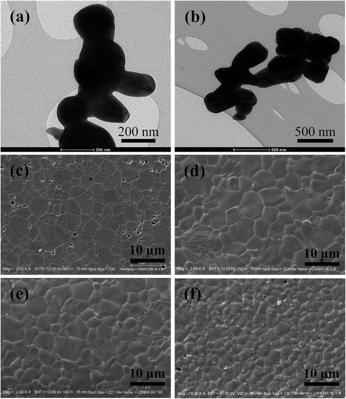
The XRD patterns of the sintered La1.7Sr0.3Ni1−xMgxO4 (M-LSNO) ceramics, where x = 0, 0.3, 0.4 and 0.5, are shown in Fig. 1a, confirming the formation of an LSNO phase (JCPDS 32-1241) with a tetragonal structure. The identified crystal structure and the detected XRD patterns were similar to those reported in previous studies.6,7,9,11–14,31 No impurity phase diffraction peak was observed. Rietveld refinement profile fits were performed, as illustrated in Fig. 1b. Accordingly, lattice parameters of La1.7Sr0.3Ni1−xMgxO4 ceramics with x = 0, 0.3, 0.4 and 0.5 were obtained to be a = 3.8306 and c = 12.7115 Å, a = 3.8371 and c = 12.7234 Å, a = 3.8463 and c = 12.7429 Å and a = 3.8653 and c = 12.8225 Å, respectively. These values are comparable to JCPDS 32-1241 for a = 3.817 and c = 12.766 Å and literature values [a = 3.8167 and c = 12.7410 Å].9,10,15,18,19 The effect of Mg2+ dopant on the crystal structure of LSNO ceramics is demonstrated in Fig. 1c. Both of a and c values of the La1.7Sr0.3Ni1−xMgxO4 ceramics increases with increasing Mg2+ dopant (x). The increased lattice parameters were primarily attributed to the larger ionic radius of the Mg2+ dopant (r4 = 0.57 Å) compared to that of the host Ni2+ ion (r4 = 0.55 Å). The crystal structure of La1.7Sr0.3Ni1−xMgxO4 is illustrated in Fig. 1d.Nanosized-La1.7Sr0.3Ni1−xMgxO4 powders (x = 0 and 0.4) with grain sizes of about 200–400 nm are shown in Fig. 2a and b. The polished-surfaces of the sintered ceramics using these powders are shown in Fig. 2c–f. The grain size of the sintered LSNO ceramics was slightly enlarged by doping with Mg2+ ions with x = 0–0.4. However, the grain size of the La1.7Sr0.3Ni1−xMgxO4 ceramic with x = 0.5 was significantly reduced. A large number of pores were observed in the microstructure of undoped-LSNO ceramics, while the La1.7Sr0.3Ni1−xMgxO4 ceramics with x = 0.3–0.5 had a dense microstructure with no pores. The relative densities of the La1.7Sr0.3Ni1−xMgxO4 ceramics with x = 0, 0.3, 0.4 and 0.5 were calculated using the Archimedes method and found to be ≈73, ≈87, ≈86, and ≈90%, respectively. It is likely that doping with Mg2+ ions caused an increase in densification of LSNO ceramics.
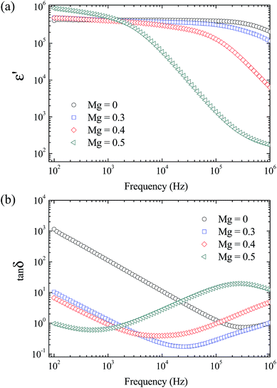
The giant dielectric properties in the frequency range of 102 to 106 Hz for the sintered La1.7Sr0.3Ni1−xMgxO4 ceramics were studied at RT, as shown in Fig. 3. All of the ceramics exhibited giant ε′ values of about 105 to 106 in a low-frequency range. At 102 Hz, the ε′ values of the La1.7Sr0.3Ni1−xMgxO4 ceramics with x = 0–0.4 were nearly identical [Fig. 3a]. The ε′ value at 1 kHz increased from ≈4.3 × 10⁵ to ≈5.1 × 10⁵ as x increased from 0–0.5. The difference in the frequency dependence of ε′ and tan![[thin space (1/6-em)]](https://www.rsc.org/images/entities/char_2009.gif) δ for the La1.7Sr0.3Ni1−xMgxO4 ceramics with different x values was observed. In the frequency range of 102 to 105 Hz, ε′ of the La1.7Sr0.3Ni1−xMgxO4 ceramic with x = 0 was independent of frequency. ε′ began to decrease to a lower value when the frequency was increased to 106 Hz. A step-like decrease in ε′ (or a critical response frequency) of La1.7Sr0.3Ni1−xMgxO4 ceramics shifted to lower frequencies as x increased. This result is similar to that observed in Al-doped LSNO (ref. 10) and Al-doped Sm1.5Sr0.5NiO4 (ref. 32) ceramics. As shown in Fig. 3b, tan
δ for the La1.7Sr0.3Ni1−xMgxO4 ceramics with different x values was observed. In the frequency range of 102 to 105 Hz, ε′ of the La1.7Sr0.3Ni1−xMgxO4 ceramic with x = 0 was independent of frequency. ε′ began to decrease to a lower value when the frequency was increased to 106 Hz. A step-like decrease in ε′ (or a critical response frequency) of La1.7Sr0.3Ni1−xMgxO4 ceramics shifted to lower frequencies as x increased. This result is similar to that observed in Al-doped LSNO (ref. 10) and Al-doped Sm1.5Sr0.5NiO4 (ref. 32) ceramics. As shown in Fig. 3b, tan![[thin space (1/6-em)]](https://www.rsc.org/images/entities/char_2009.gif) δ of the undoped-LSNO ceramic (x = 0) increased sharply, by about two orders of magnitude, as the frequency was decreased from 104 to 102 Hz. This behavior is generally considered the effect of DC conduction in the bulk ceramics and/or the effect of non-ohmic sample-electrode contact.33–35 It was also found that, for the ceramics with x = 0–0.4, tan
δ of the undoped-LSNO ceramic (x = 0) increased sharply, by about two orders of magnitude, as the frequency was decreased from 104 to 102 Hz. This behavior is generally considered the effect of DC conduction in the bulk ceramics and/or the effect of non-ohmic sample-electrode contact.33–35 It was also found that, for the ceramics with x = 0–0.4, tan![[thin space (1/6-em)]](https://www.rsc.org/images/entities/char_2009.gif) δ increased sharply with increasing frequency in a high frequency range, corresponding to a rapid decrease in ε′. For the ceramic with x = 0.5, the critical response frequency was the lowest and a corresponding tan
δ increased sharply with increasing frequency in a high frequency range, corresponding to a rapid decrease in ε′. For the ceramic with x = 0.5, the critical response frequency was the lowest and a corresponding tan![[thin space (1/6-em)]](https://www.rsc.org/images/entities/char_2009.gif) δ-peak appeared. This behavior indicated that a dielectric relaxation mechanism exists in the bulk ceramic under an applied AC electric field. According to the small polaronic model,11,19,32 the decrease in a critical response frequency of the M-LSNO ceramic with x = 0.5 can be ascribed to the effect of polaronic size, which may be increased by doping with a high concentration of Mg2+ ions. Alternatively, it is possible but unlikely that this dielectric relaxation behavior can be described based on the electrode effect or that the electrode effect may be quite small in M-LSNO ceramics with high concentrations of Mg2+ ions.
δ-peak appeared. This behavior indicated that a dielectric relaxation mechanism exists in the bulk ceramic under an applied AC electric field. According to the small polaronic model,11,19,32 the decrease in a critical response frequency of the M-LSNO ceramic with x = 0.5 can be ascribed to the effect of polaronic size, which may be increased by doping with a high concentration of Mg2+ ions. Alternatively, it is possible but unlikely that this dielectric relaxation behavior can be described based on the electrode effect or that the electrode effect may be quite small in M-LSNO ceramics with high concentrations of Mg2+ ions.
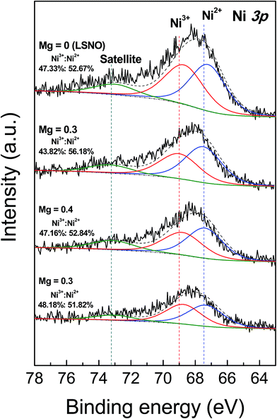
To clarify the effect of Mg2+ doping ions on the small polaronic hopping behavior in LSNO ceramics, all the sintered ceramics were characterized by XPS. Fig. 4 shows the XPS spectra of Ni 3p regions of the sintered La1.7Sr0.3Ni1−xMgxO4 (M-LSNO) ceramics with x = 0, 0.3, 0.4 and 0.5. The Ni 3p peaks of all sintered ceramics can be deconvoluted into three main peaks. The peaks at ≈67.2–67.5 eV are assigned to Ni2+,36 while the peaks at ≈68.7–69.0 eV are attributed to Ni3+. The peaks at ≈73.0–73.3 eV are assigned to a satellite peak associated with Ni2+. This observation is consistent with that reported in literature.37 The result confirms the coexistence of Ni2+ and Ni3+ in the samples. The presence of Ni3+ indicated that the conduction was attributable to charge hopping between Ni3+ ↔ Ni2+. As shown in Fig. 4, the ratios of Ni3+/Ni2+ in the undoped-LSNO ceramic and M-LSNO ceramics with x = 0.3, 0.4 and 0.5 changed slightly. This means that Mg2+ ions preferentially substituted into Ni2+ sites. It is reasonable to suggest that the small polaronic concentration the M-LSNO ceramics should not significantly change. This result is consistent with the observed GDR in M-LSNO ceramics, in which the ε′ value in a low frequency range was not decreased by Mg2+ doping. Changes in the critical response frequency were likely due to an increase in polaronic sizes, just as was proposed in Al-doped LSNO ceramics.6
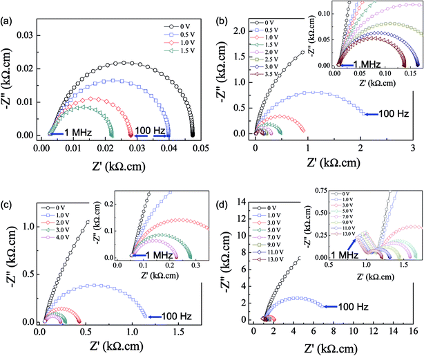
The small polaronic hopping mechanism or the electrode effect is now the most likely origin of the GDR in LSNO ceramics.10,15,32 Electrical conduction inside the grains is therefore considered the primary factor. In the M-LSNO ceramics, however, the GB response may be another important factor. This is because the large decrease in tan![[thin space (1/6-em)]](https://www.rsc.org/images/entities/char_2009.gif) δ may have been caused by the dominant effect of the GB response. Impedance spectroscopy is a powerful tool for separating the electrical responses of grains, GB and the electrode effect.22,28,29 It was used to determine the total resistance, which can be estimated from a large semicircular arc. Total resistance increases with increasing Mg2+ dopant concentration [Fig. 5]. A Z* plot of the M-LSNO ceramic with x = 0 (undoped-LSNO) cannot be seen in Fig. 5 and inset (a). This was due to its very low total resistance compared to that of the other ceramics [inset (b)]. Furthermore, a nonzero intercept on the Z′ axis was observed, indicating that there exists some component of the ceramic with relatively low conductivity, which may be the grains. Usually, Rg values at RT of LSNO ceramics are about 0.1–2.5 Ω cm.32 This is quite consistent with the value obtained from the observed nonzero intercept, which corresponds to Rg. The total resistance is usually governed by Rgb or Rgb + Re. Generally, the grain (bulk), GB, and electrode responses can each be described by a parallel R–C element, whereas the macroscopic dielectric response is usually represented by a series connection of three R–C elements.38 To clarify, impedance data were fitted to a single R–C parallel circuit for a Z* plot,
δ may have been caused by the dominant effect of the GB response. Impedance spectroscopy is a powerful tool for separating the electrical responses of grains, GB and the electrode effect.22,28,29 It was used to determine the total resistance, which can be estimated from a large semicircular arc. Total resistance increases with increasing Mg2+ dopant concentration [Fig. 5]. A Z* plot of the M-LSNO ceramic with x = 0 (undoped-LSNO) cannot be seen in Fig. 5 and inset (a). This was due to its very low total resistance compared to that of the other ceramics [inset (b)]. Furthermore, a nonzero intercept on the Z′ axis was observed, indicating that there exists some component of the ceramic with relatively low conductivity, which may be the grains. Usually, Rg values at RT of LSNO ceramics are about 0.1–2.5 Ω cm.32 This is quite consistent with the value obtained from the observed nonzero intercept, which corresponds to Rg. The total resistance is usually governed by Rgb or Rgb + Re. Generally, the grain (bulk), GB, and electrode responses can each be described by a parallel R–C element, whereas the macroscopic dielectric response is usually represented by a series connection of three R–C elements.38 To clarify, impedance data were fitted to a single R–C parallel circuit for a Z* plot,
 | (1) |
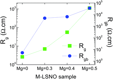
It is notable that the capacitance of the non-ohmic sample-electrode contact (Ce = 1/2πfmaxRe) was ≈4.8 × 10⁻⁸ F, which was lower than that of the apparent capacitance of the sample (≈1.2 × 10⁻⁷ F at 1 kHz). This indicates that there is another source of polarization contributing to the overall GDR in the undoped-LSNO ceramic. Interfacial polarization at the GBs can be ruled out because Rgb (≈5.34 Ω cm) was just slightly larger than Rg (≈2.65 Ω cm). Thus, the polaronic hopping process is the most probable factor contributing to the overall GDR in the undoped-LSNO ceramic coupled with the electrode effect, but its intensity was too great. In inset (a) of Fig. 5, a relatively small semicircular arc was observed in the Z* plot of the M-LSNO ceramic with x = 0.5 that could be ascribed to the grain response with Rg ≈ 1120 Ω cm (at RT). This value is comparable to Rg ≈ 1100 Ω (at 300 K) for Sm1.5Sr0.5Ni0.5Al0.5O4 ceramic32 and Rg ≈ 2663 Ω (at 300 K) for La1.75Sr0.25Ni0.7Al0.3O4 ceramic.6 According to the Z* plot of the M-LSNO ceramic with x = 0.5, the large semicircular arc can be ascribed to the RgbCgb response, since the ReCe response was less dominant due to large increases in Rg and Rgb.22,23 Thus, it is reasonable that Rg and Rgb of the M-LSNO ceramics increased with increasing Mg2+ dopant concentration, as shown in Fig. 6.
The Rg values of the M-LSNO ceramics with x = 0.3, 0.4 and 0.5 were, respectively, enhanced by factors of ≈2, ≈21 and ≈422 compared to that of the undoped-LSNO ceramic. As represented in Fig. 4, giving a real overall composition of La1.7Sr0.3(Ni2+, Ni3+)1−xMgxO4, the amount of both Ni2+ and Ni3+ ions decreased with increasing Mg2+ dopant concentration because of a slight change in the ratios of Ni3+/Ni2+ for all ceramics. The conductivity of M-LSNO ceramics, which was primarily caused by charge hopping between Ni3+ ↔ Ni2+ ions, was decreased due to reduction in concentration of charge carriers. It is notable that the total amount of Ni2+ and Ni3+ ions and the amount of Mg2+ dopant ions are the same in value for the M-LSNO ceramic with x = 0.5. Therefore, the long range motion of hopping charges inside the grains was also strongly inhibited by Mg2+ ions.
It was also observed that the Rgb value of the M-LSNO ceramic with x = 0.5 was much larger than that of the ceramics with x = 0.3 and 0.4. The GB response in M-LSNO ceramics was dominant and the total resistance is therefore governed by Rgb. Substitution of Mg2+ into LSNO ceramics can cause a great increase in Rgb. Usually, both of the intrinsic and geometric factors have an influence on the electrical properties of the GBs. As clearly shown in the SEM images, the grain size of the M-LSNO ceramic with x = 0.5 was significantly reduced. This is the primary cause of the remarkable increase in Rgb due to the increase in insulating GB layers. Accordingly, the significant decrease in tan![[thin space (1/6-em)]](https://www.rsc.org/images/entities/char_2009.gif) δ in a low-frequency range for M-LSNO ceramics was clearly due to the large increase in Rgb.
δ in a low-frequency range for M-LSNO ceramics was clearly due to the large increase in Rgb.
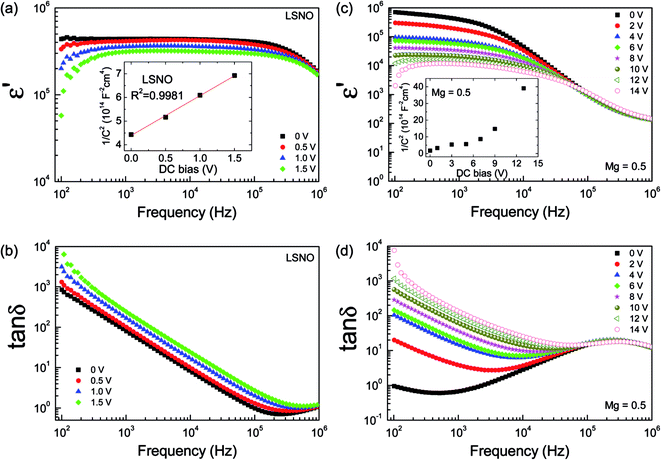
Generally, investigation of the electrical and dielectric properties under different DC bias voltages can be done to analyze the electrical responses of GB and electrode effects.28,29 As shown in Fig. 7a, the observed semicircular arc of the undoped-LSNO ceramic decreased with increasing DC bias. As previously discussed, such a semicircular arc may have been due to the ReCe response. This was confirmed using a Mott–Schottky plot of 1/C2 vs. DC bias voltage, as shown in the inset of Fig. 8a. It showed a linear response, i.e., variation in the capacitance value with DC bias obeys the Mott–Schottky law for the formation Schottky barrier between metal electrodes and a semiconducting surface.29
In Fig. 7b and c, the semicircular arc of the M-LSNO ceramics with x = 0.3 and 0.4 decreased with increasing DC bias voltage, while the nonzero intercept did not change as shown in the insets. The Rgb values of the M-LSNO ceramics with x = 0.3 and 0.4 were enhanced by factors of ≈930 and ≈1200, respectively, compared that of the undoped-LSNO ceramic. These Rgb values were much larger than that of Re of the undoped-LSNO ceramic. When Rgb ≫ Re, the electrode effect was dominant in these samples.22 In Fig. 7d and its inset, the Rgb of the M-LSNO ceramic with x = 0.5 was greatly reduced from 36 kΩ cm to 222 Ω cm by increasing the DC bias from 0 to 13 V, while Rg decreased slightly from 1120 to 1009 Ω cm. The reduction in Rg may have been caused by injected electrons, which were trapped by oxygen vacancies or other defects.39 A Mott–Schottky plot of 1/C2 (extracted from the large arc in the Z* plots) vs. DC bias voltage showed a nonlinear response (inset of Fig. 8c). Therefore, the electrode effect can be excluded as the origin of this electrical response. The GB capacitance of the M-LSNO ceramic with x = 0.5 was extracted from Z* plots (Cgb = 1/2πfmaxRgb) and found to be ≈7.5 × 10⁻⁸ F. This was lower than that of the apparent capacitance value of the sample (≈1.2 × 10⁻⁷ F at 1 kHz). In contrast to the undoped-LSNO ceramic, further contribution from the electrode effect can be ignored because Rgb ≫ Re. The polaronic hopping process is also hypothesized as another important factor contributing to the GDR in the M-LSNO ceramic with x = 0.5 as well as in the x = 0.3 and 0.4 samples.
As illustrated in Fig. 8a and b, the ε′ value over the measured frequency range of the undoped-LSNO ceramic decreased as the DC bias was increased from 0–1.5 V, while tan![[thin space (1/6-em)]](https://www.rsc.org/images/entities/char_2009.gif) δ increased. These results were due to the decrease in Schottky barrier height at the sample-electrode contact as a result of the effect of DC bias. When the DC bias was increased to 2 V, an overload limited measurement occurred. The overload DC bias was at 15 V. This occurred in the M-LSNO ceramic with x = 0.5, but only in the frequency range below 104 Hz. However, the mechanisms in these two cases were totally different. The mechanisms in the former and later ceramics were correlated with the electrical responses at the sample-electrode contact and GBs, respectively.
δ increased. These results were due to the decrease in Schottky barrier height at the sample-electrode contact as a result of the effect of DC bias. When the DC bias was increased to 2 V, an overload limited measurement occurred. The overload DC bias was at 15 V. This occurred in the M-LSNO ceramic with x = 0.5, but only in the frequency range below 104 Hz. However, the mechanisms in these two cases were totally different. The mechanisms in the former and later ceramics were correlated with the electrical responses at the sample-electrode contact and GBs, respectively.
4. Conclusions
The origins of the giant dielectric responses in LSNO ceramics were demonstrated via DC bias measurements. For the undoped-LSNO ceramic, the giant ε′ and Re values decreased with increasing DC bias over the measured frequency range, while tan![[thin space (1/6-em)]](https://www.rsc.org/images/entities/char_2009.gif) δ linearly increased. Furthermore, the decreased C values with increasing DC bias voltage were found to follow the Mott–Schottky law, confirming the dominant electrode effect. By comparing the apparent C value of the sintered ceramic with Ce value extracted from IS analysis, the giant ε′ response in the undoped-LSNO ceramic can be attributed to the electrode effect and the small polaronic hopping mechanism. For M-LSNO ceramics, changes in ε′, Rgb and tan
δ linearly increased. Furthermore, the decreased C values with increasing DC bias voltage were found to follow the Mott–Schottky law, confirming the dominant electrode effect. By comparing the apparent C value of the sintered ceramic with Ce value extracted from IS analysis, the giant ε′ response in the undoped-LSNO ceramic can be attributed to the electrode effect and the small polaronic hopping mechanism. For M-LSNO ceramics, changes in ε′, Rgb and tan![[thin space (1/6-em)]](https://www.rsc.org/images/entities/char_2009.gif) δ were similar to those observed in an undoped-LSNO ceramic. However, a linear Mott–Schottky plot of 1/C2 vs. DC bias voltage was not obtained, indicating that the electrode effect was not dominant in the M-LSNO ceramics due to a large increase in Rgb. The origins of the giant ε′ behavior in M-LSNO ceramics can be well described based on the Maxwell–Wagner polarization at insulating GBs and the small polaronic hopping mechanism.
δ were similar to those observed in an undoped-LSNO ceramic. However, a linear Mott–Schottky plot of 1/C2 vs. DC bias voltage was not obtained, indicating that the electrode effect was not dominant in the M-LSNO ceramics due to a large increase in Rgb. The origins of the giant ε′ behavior in M-LSNO ceramics can be well described based on the Maxwell–Wagner polarization at insulating GBs and the small polaronic hopping mechanism.
Acknowledgements
This work was financially supported by the Thailand Research Fund (TRF) and Khon Kaen University, Thailand [Grant No. RSA5880012]. The authors would like to thank the SUT-NANOTEC-SLRI (BL5.1) Joint Research Facility for use of their XPS facility. K. Meeporn would like to thank the Thailand Research Fund through the Royal Golden Jubilee PhD Program (Grant No. PHD/0191/2556) for his PhD scholarship.References
- X. Q. Liu, S. Y. Wu, X. M. Chen and H. Y. Zhu, J. Appl. Phys., 2008, 104, 054114 CrossRef.
- S. Krohns, P. Lunkenheimer, C. Kant, A. V. Pronin, H. B. Brom, A. A. Nugroho, M. Diantoro and A. Loidl, Appl. Phys. Lett., 2009, 94, 122903 CrossRef.
- X. Q. Liu, Y. J. Wu and X. M. Chen, Solid State Commun., 2010, 150, 1794–1797 CrossRef CAS.
- B. W. Jia, W. Z. Yang, X. Q. Liu and X. M. Chen, J. Appl. Phys., 2012, 112, 024104 CrossRef.
- A. Podpirka and S. Ramanathan, J. Appl. Phys., 2011, 109, 014106 CrossRef.
- X. Q. Liu, S. Y. Wu and X. M. Chen, J. Alloys Compd., 2010, 507, 230–235 CrossRef CAS.
- X. Q. Liu, Y. J. Wu, X. M. Chen and H. Y. Zhu, J. Appl. Phys., 2009, 105, 054104 CrossRef.
- P. Thongbai, T. Yamwong and S. Maensiri, Mater. Lett., 2012, 82, 244–247 CrossRef CAS.
- K. Meeporn, T. Yamwong and P. Thongbai, Jpn. J. Appl. Phys., 2014, 53, 06JF01 CrossRef.
- A. Chouket, O. Bidault, V. Optasanu, A. Cheikhrouhou, W. Cheikhrouhou-Koubaa and M. Khitouni, RSC Adv., 2016, 6, 24543–24548 RSC.
- X. Q. Liu, G. Liu, P. P. Ma, G. J. Li, J. W. Wu and X. M. Chen, J. Electroceram., 2016 DOI:10.1007/s10832-016-0041-2.
- T. I. Chupakhina, N. I. Kadyrova, N. V. Melnikova, O. I. Gyrdasova, E. A. Yakovleva and Y. G. Zainulin, Mater. Res. Bull., 2016, 77, 190–198 CrossRef CAS.
- A. Chouket, W. Cheikhrouhou-Koubaa, A. Cheikhrouhou, V. Optasanu, O. Bidault and M. Khitouni, J. Alloys Compd., 2016, 662, 467–474 CrossRef CAS.
- A. Chouket, V. Optasanu, O. Bidault, A. Cheikhrouhou, W. Cheikhrouhou-Koubaa and M. Khitouni, J. Alloys Compd., 2016, 688, 163–172 CrossRef CAS.
- M. Li and D. C. Sinclair, J. Appl. Phys., 2012, 111, 054106 CrossRef.
- E. Winkler, F. Rivadulla, J. S. Zhou and J. B. Goodenough, Phys. Rev. B: Condens. Matter Mater. Phys., 2002, 66, 094418 CrossRef.
- G. Liu, X. Q. Liu and X. M. Chen, Appl. Phys. A: Mater. Sci. Process., 2014, 116, 1421–1427 CrossRef CAS.
- G. Liu, T. T. Chen, J. Wang, X. Q. Liu and X. M. Chen, J. Alloys Compd., 2013, 579, 502–506 CrossRef CAS.
- J. Wang, G. Liu, B. W. Jia, X. Q. Liu and X. M. Chen, Ceram. Int., 2014, 40, 5583–5590 CrossRef CAS.
- X. Huang, H. Zhang, J. Li and Y. Lai, J. Mater. Sci.: Mater. Electron., 2016, 1–7 Search PubMed.
- S. Wu, P. Liu, Y. Lai, W. Guan, Z. Huang, J. Han, Y. Xiang, W. Yi and Y. Zeng, J. Mater. Sci.: Mater. Electron., 2016, 1–6 Search PubMed.
- M. Li, D. C. Sinclair and A. R. West, J. Appl. Phys., 2011, 109, 084106 CrossRef.
- M. Li, Z. Shen, M. Nygren, A. Feteira, D. C. Sinclair and A. R. West, J. Appl. Phys., 2009, 106, 104106 CrossRef.
- L. Sun, R. Zhang, Z. Wang, E. Cao, Y. Zhang and L. Ju, J. Alloys Compd., 2016, 663, 345–350 CrossRef CAS.
- A. Nautiyal, C. Autret, C. Honstettre, S. De Almeida-Didry, M. El Amrani, S. Roger, B. Negulescu and A. Ruyter, J. Eur. Ceram. Soc., 2016, 36, 1391–1398 CrossRef CAS.
- J. Boonlakhorn and P. Thongbai, Jpn. J. Appl. Phys., 2015, 54, 06FJ06 CrossRef.
- J. Boonlakhorn, P. Kidkhunthod and P. Thongbai, J. Eur. Ceram. Soc., 2015, 35, 3521–3528 CrossRef CAS.
- T. Adams, D. Sinclair and A. West, Phys. Rev. B: Condens. Matter Mater. Phys., 2006, 73, 094124 CrossRef.
- M. Li, A. Feteira and D. C. Sinclair, J. Appl. Phys., 2009, 105, 114109 CrossRef.
- P. Thongbai, T. Yamwong and S. Maensiri, Appl. Phys. Lett., 2009, 94, 152905 CrossRef.
- C. L. Song, Y. J. Wu, X. Q. Liu and X. M. Chen, J. Alloys Compd., 2010, 490, 605–608 CrossRef CAS.
- X. Q. Liu, B. W. Jia, W. Z. Yang, J. P. Cheng and X. M. Chen, J. Phys. D: Appl. Phys., 2010, 43, 495402 CrossRef.
- K. Meeporn, T. Yamwong, S. Pinitsoontorn, V. Amornkitbamrung and P. Thongbai, Ceram. Int., 2014, 40, 15897–15906 CrossRef CAS.
- J. Boonlakhorn and P. Thongbai, J. Electron. Mater., 2015, 44, 3687–3695 CrossRef CAS.
- B. Wen Jia, X. Qiang Liu and X. Ming Chen, J. Appl. Phys., 2011, 110, 064110 CrossRef.
- A. N. Mansour, Surf. Sci. Spectra, 1994, 3, 231–238 CrossRef CAS.
- A. N. Mansour, Surf. Sci. Spectra, 1994, 3, 279–286 CrossRef CAS.
- R. Schmidt, M. C. Stennett, N. C. Hyatt, J. Pokorny, J. Prado-Gonjal, M. Li and D. C. Sinclair, J. Eur. Ceram. Soc., 2012, 32, 3313–3323 CrossRef CAS.
- Y. Song, X. Wang, Y. Sui, Z. Liu, Y. Zhang, H. Zhan, B. Song, Z. Liu, Z. Lv, L. Tao and J. Tang, Sci. Rep., 2016, 6, 21478 CrossRef CAS PubMed.
| This journal is © The Royal Society of Chemistry 2016 |


