
 Open Access Article
 This Open Access Article is licensed under a
 Creative Commons Attribution 3.0 Unported Licence
Femtosecond laser nanowelding of silver nanowires for transparent conductive electrodes†
Jeonghong Haa,
Bong Jae Leeb,
David J. Hwangc and
Dongsik Kim*a
aDepartment of Mechanical Engineering, POSTECH, Pohang, 790-784, Republic of Korea. E-mail: dskim87@postech.ac.kr
bDepartment of Mechanical Engineering, Korea Advanced Institute of Science and Technology (KAIST), Daejeon 305-701, Republic of Korea
cDepartment of Mechanical Engineering, Stony Brook University, NY 11794, USA
First published on 5th September 2016
Abstract
This work reports a method for nanowelding silver nanowires (AgNWs) using ultrashort laser pulses to minimize thermal damage on flexible substrates. Because of localized field enhancement and limited thermal diffusion, femtosecond laser irradiation enabled joining of AgNWs only at junctions, maintaining their original crystalline structure. The femtosecond laser nanowelding process produced neither breakup of the nanowire (NW) junction nor thermal aggregation. In addition, the sheet resistance and transmittance of the AgNW network were improved up to 25 Ω sq−1 and over 94% at 550 nm, respectively. The femtosecond laser irradiation caused considerably less damage to a polymer substrate than nanosecond laser irradiation. The proposed nanowelding process is expected to serve as a useful tool to fabricate integrated plasmonic devices as well as transparent conducting electrodes on flexible substrates.
Introduction
Silver nanowire (AgNW) networks have recently attracted substantial attention as an alternative to indium tin oxide films owing to their good electrical, optical, and mechanical properties.1–3 However, electrical conduction in nanowire (NW) networks is limited by wire-to-wire junction resistance,3,4 which can result in high resistivity, electric failure, and thermal stress.5,6 Therefore, there is an emerging need to develop technology for joining NW junctions effectively, especially in scalable fabrication of future electronics. Significant success has been reported in fusing wire-to-wire junction using various methods including thermal annealing,3,7 mechanical pressing,8 Joule heating,9,10 and plasmonic optical welding.11Recently, an optical welding technique has been reported using a broadband continuous wave light source. They demonstrated that the electromagnetic field enhanced in the nanoscale gap between two crossing AgNWs could be employed to weld the AgNWs. The optical welding technique can induce localized heat generation at the junction while thermal annealing heats NWs uniformly.11 High-intensity pulsed lasers were also employed owing to their advantages such as a localized thermal effect and a fine spatial resolution.12–16
Successful nanowelding of AgNWs using nanosecond or longer pulsed lasers has been reported, showing good electrical conductivity and formation of localized junctions at contact points.12–16 However, those processes generated knurls on AgNW surface,12 deformation of the polyethylene terephthalate (PET) substrate,12 degradation of transmittance,13 or balling at the ends of AgNWs.14 A recent work demonstrated successful joining of AgNWs without affecting the AgNWs network other than the junctions using a KrF excimer laser (248 nm, 25 ns, 20 mJ cm−2).15 One potential problem is that the process may cause surface damage on flexible substrates. For example, the damage and ablation thresholds of PET by excimer laser irradiation are 5 and 22 mJ cm−2, respectively.17–19
A femtosecond laser is a unique tool in nanoscopic processing of materials as it can deposit energy with a time scale shorter than the electron–phonon equilibrium time.20 Accordingly, femtosecond laser irradiation can offer high-intensity material processing with a nanoscale precision.21–23 Although near-field optical excitation may result in highly localized heating at discrete points of a nanostructure, the equilibrium temperature distribution in the nanostructure becomes almost uniform as the thermal diffusion length exceeds the dimension of the sample even for nanosecond laser pulses.24 On the contrary, femtosecond pulses enable localized heating because thermal effects can be frozen near the location of initial energy deposition.25,26 Furthermore, femtosecond laser irradiation can lead a material to a highly nonequilibrium state, possibly inducing nonthermal phase transformations. For instance, at a laser fluence close to the surface damage threshold, strong electronic excitation followed by weakening the interatomic bonds may occur, causing a nonthermal phase transition.27,28 Previous studies also showed theoretically and experimentally that nanoparticles can be melted at a temperature below the conventional thermal melting point and joined together with a melting thickness of a few nanometers using ultrafast laser irradiation.26,29,30
In this work, we report our attempt to develop a nanowelding process for AgNWs using femtosecond laser pulses. More specifically, our aim was to generate nanowelded AgNW junctions without affecting other region of the nanowire network and the PET substrate. In addition to the formation of crystalline structures at each junction, the sheet resistance and transmittance of the fabricated AgNW films were also measured to assess the feasibility of the fabrication of transparent conducting electrodes on flexible PET substrates. Morphological changes were investigated using scanning electron microscopy (SEM) and transmission electron microscopy (TEM) before and after laser irradiation. We performed numerical simulations to investigate the localized field enhancement and the heat diffusion based on two-temperature model.
Materials and methods
Materials
AgNW dispersion (1 wt%, 30–40 nm diameter, 10–20 μm length, purity > 99.9%) was purchased from Ditto Technology. The mean diameter of the NWs determined from SEM images was 38.0 ± 2.7 nm before laser irradiation. Before the deposition of the AgNWs on the PET substrates, the AgNW dispersion was homogenized using a magnetic stirrer for 1 h. The AgNWs were deposited on the PET substrates using spin coating at 1800 rpm for 45 s. Then the sample was dried in the ambient air environment at room temperature (20 °C) for 10 min. The spin-coated samples maintained good adhesion characteristics without any degradation of sheet resistance. No detachment of AgNWs was observed unless the layer was mechanically scratched.Laser irradiation
A femtosecond Ti:sapphire laser with a regenerative amplification system (wavelength λ = 800 nm, full width at half maximum FWHM = 50 fs, pulse energy < 3.5 mJ, repetition rate = 1 kHz) was employed in the experiment. The laser beam was linearly polarized with a Gaussian energy distribution (M squared factor < 1.2). A half-wave plate and a polarizer were used to adjust the laser pulse energy. After passing through a square shaped aperture of 3 mm by 3 mm, the laser beam was projected by a lens with a focal length of 150 mm. The sample was placed perpendicular to the laser beam at 3 mm after focal point, and the measured laser spot size was 500 μm. The laser beam scanned the sample surface by moving the sample stage using a computer-controlled microstage. The scanning speed (v) was varied in the range of 0.1–10 mm s−1 at a pulse repetition rate of 1 kHz. Correspondingly, each spot was irradiated with 50–5000 laser pulses effectively using the beam scanning method.To clarify the effect of ultrafast laser irradiation on the nanowelding process, experiments were carried out using a nanosecond laser (KrF excimer laser of λ = 248 nm, FWHM = 25 ns) for comparison.
Characterization
A four-point probe system was employed to measure the sheet resistance of the sample before and after the laser treatment. The sample (20 mm by 20 mm) was probed with 1 mm tip spacing. Transmittance spectra were obtained using an ultraviolet-visible-near-infrared spectrometer (V670, JASCO Corp.) with the original PET substrate as a reference. The topography of the AgNWs was analyzed using high-resolution SEM (JEOL JSM-7401) and high-resolution TEM (HRTEM, JEOL JEM-2200FS). The TEM sample was prepared by drop-casting on silicon dioxide TEM grid. The morphology of substrate was analyzed using an atomic force microscope (AFM, VEECO Dimension 3100).Results and discussion
Sheet resistance and transmittance
Fig. 1a shows the sheet resistance and transmittance of the AgNW films before and after femtosecond laser irradiation for various fluences (F) at a fixed scan speed (v) of 0.1 mm s−1. The measurements were repeated 10 times for each sample at random positions. The error bars in Fig. 1a indicate the standard deviation of the measured data. The spin-coated AgNW layer before laser irradiation has a sheet resistance of 87 Ω sq−1 and a transmittance of 91.3% at 633 nm. The sheet resistance/transmittance level indicates that polyvinyl pyrrolidone (PVP) barely exists in the pristine AgNW, which was confirmed by TEM images. After laser irradiation, the sheet resistance of the film was substantially reduced. At F = 30 mJ cm−2, neither the sheet resistance nor the transmittance changed significantly. When 30 mJ cm−2 ≤ F ≤ 120 mJ cm−2, the sheet resistance decreased and the lowest sheet resistance was 25 Ω sq−1 at F = 90 mJ cm−2. The transmittance remained the same or slightly increased, yielding a maximum value of 94.3% at F = 90 mJ cm−2. When F > 180 mJ cm−2, the sheet resistance increased and the transmittance decreased significantly. Fig. 1b shows the sheet resistance of the AgNW films at various scan speeds and fluences. At F = 45 and 90 mJ cm−2, the sheet resistance increased with increasing the scan speed. At F = 180 mJ cm−2, the sheet resistance increased with decreasing the scan speed. Fig. 1c shows the optical transparency before and after laser treatment for various laser fluences at v = 0.1 mm s−1. Consequently, in this work, the optimal condition for fabricating a conducting transparent AgNW film was F ∼ 90 mJ cm−2 and v ∼ 0.1 mm s−1 (Fig. 1b). These results indicate that femtosecond laser irradiation can serve as an effective tool to fabricate AgNW thin films on flexible substrates with high conductivity and transmittance (Fig. 1d). | ||
| Fig. 1 Sheet resistances and transmittances of the AgNW films before and after femtosecond laser irradiation at (a) various laser fluences (scan speed = 0.1 mm s−1) and (b) scan speeds. (c) The transmittance spectra of the AgNW films on the PET substrate after laser irradiation and (d) comparison of the transmittance and sheet resistance with the previously reported results. | ||
Morphology of the laser-welded AgNWs
The SEM images of AgNWs spin-coated on the silicon substrate before and after laser treatment (v = 0.1 mm s−1) are displayed in Fig. 2. Fig. 2a displays AgNWs randomly deposited with network formation. We did not observe any notable change in the SEM images at F < 90 mJ cm−2 (Fig. S1†). After laser treatment at F = 90 mJ cm−2, the contact points began to fuse (Fig. 2b). A higher laser fluence (F = 120 mJ cm−2) starts to cause damage of several AgNWs (Fig. 2c). Further increase in the laser fluence to F = 180 mJ cm−2 substantially induced damage and breakup of the AgNWs (Fig. 2d), which is consistent with a steep increase in the sheet resistance (Fig. 1a). In addition to SEM, TEM analysis was performed to observe a change at the AgNW contact caused by laser irradiation. Before laser irradiation, each AgNW lied on another one without forming atomic bonds (Fig. 3a). After laser treatment, the AgNWs formed an intimate contact and/or welding (Fig. 3b).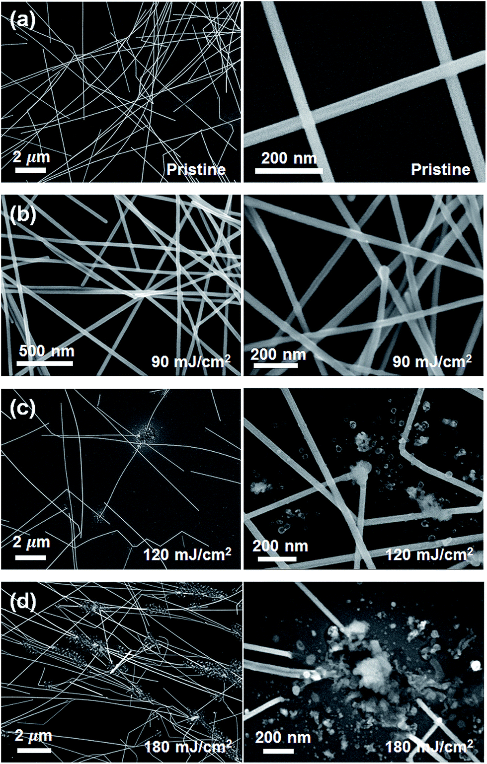 | ||
| Fig. 2 SEM images of the AgNW films on the silicon substrate (a) before and after laser irradiation at various fluences, (b) F = 90 mJ cm−2, (c) 120 mJ cm−2, and (d) 180 mJ cm−2 (v = 0.1 mm s−1). The scale bars on the left and on the right are 2 μm and 200 nm, respectively. | ||
 | ||
| Fig. 3 TEM images of silver nanowire junction (a) before laser irradiation and (b) after laser irradiation at F = 90 mJ cm−2 and v = 0.1 mm s−1. | ||
Selective area electron diffraction (SAED) pattern
In order to further elucidate the femtosecond based nanowelding behavior, Fig. 4 displays the selective area electron diffraction (SAED) pattern after laser irradiation at F = 90 mJ cm−2 and v = 0.1 mm s−1. After laser treatment, the diffraction spots appeared along two directions at the junction with roughly equal intensity and rotated by approximately ninety degrees (Fig. 4d). In the case of optical welding using a halogen lamp, only a single crystal orientation exists at the junction because atoms in the bottom wire must exhibit a significant mobility and allow epitaxial recrystallization onto the top wire.11 In this work, femtosecond laser irradiation did not melt and recrystallize the entire NW, and thus recrystallization did not occur in the whole area of a NW but induced partial surface melting around the contact point maintaining the original crystal orientation of each NW. Nian et al. showed that short pulsed laser enables local crystalline nanojoining by possible nonequilibrium recrystallization rather than a epitaxial recrystallization.15 | ||
| Fig. 4 (a) High-resolution TEM image of the AgNW junction after femtosecond laser irradiation at F = 90 mJ cm−2 and v = 0.1 mm s−1. (b) The SAED pattern of the top NW far away from the junction. (c) The SAED pattern of the bottom NW far away from the junction. (d) The SAED pattern of the junction. | ||
Numerical analysis for heating the AgNWs using the laser
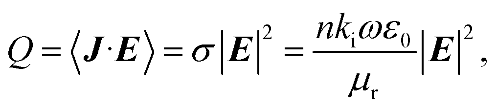
In order to examine the localized surface plasmon (LSP) resonance associated with subwavelength-sized AgNW, the absorption efficiency of a free-standing AgNW with diameter of 40 nm was calculated by finite-difference and time-domain method (Fig. S4†). For the free-standing two-dimensional AgNW under the illumination of light with the transverse-magnetic polarization, LSP occurs at 370 nm, which is far away from the wavelength of femtosecond laser. This suggests that welding of AgNW does not rely on the surface plasmon associated with an individual AgNW. Rather field localization in the vicinity of junction between two AgNWs play an important role. For verification of the field localization, we calculated the electromagnetic field distribution when two AgNWs form a junction. As can be seen from Fig. S4b,† electric field intensity is strongly enhanced in the vicinity of the junction and such field localization occurs regardless of the wavelength although enhancement factor varies.The two-dimensional finite element method (FEM) simulation was performed to calculate the electric field enhancement and heat generation (Fig. 5a and b). Maxwell's equations were solved in the frequency domain
| ∇ × (∇ × E) − nc2k02E = 0, |
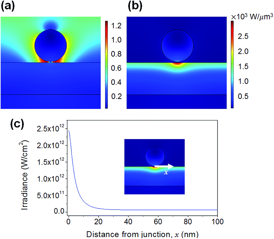 | ||
| Fig. 5 (a) Normalized electric field and (b) heat generation at the junction with a gap of 2 nm between two AgNWs with a diameter of 38 nm. The laser beam was incident from the top and polarized perpendicularly to the top NW. (c) The irradiance distribution along the surface of the bottom NW from the junction. | ||
Then the thermal transport was analyzed based on the two-temperature model (TTM). Energy dissipation in the E field can be considered as a Joule heating source
The TTM for electron and lattice temperatures Te and Tl was employed to calculate the thermal response
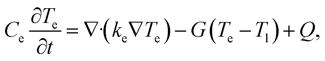
where C is the volumetric heat capacity, k is the thermal conductivity, and G is the electron–phonon coupling factor. Subscripts e and l indicate electron and lattice, respectively.
The employed TTM is based on the Fourier heat conduction theory, which is valid when a system is large enough compared to the heat-carrier mean free path.32 Although the diameter of AgNW is comparable to the mean free path of electrons (i.e. major heat-carrier for metal), the approximate temperature evolution is estimated by the TTM model assuming 55% of bulk value for thermal conductivity of AgNW in order to partly reflect the size effect.33,34 The heat generation term was taken from Fig. 5c (assumed to be localized in the distance x < 40 nm from the junction).
The temperature distribution during and after the laser irradiation shows that the thermal penetration depth (lt), over which the temperature decreases to 1/e (∼37%) of the maximum, was approximately 360 nm for femtosecond laser irradiation (pulse duration τL: 50 fs). The electron temperature increased and had the maximum value within 100 fs. Then the lattice temperature increased through electron–phonon coupling, reaching equilibrium after ∼10 ps. The lattice temperature at the junction had the maximum value after thermal equilibrium of the electron and lattice system was achieved (Fig. 6a). For comparison with nanosecond laser irradiation, we employed a laser heat source term with the same total pulse energy but different τL of 25 ns (Fig. 6b). The lattice temperature increased during laser irradiation with thermal equilibrium and had the maximum value at the junction after laser irradiation (25 ns). The thermal penetration depth was 2.5 μm, which is consistent with the estimated value using the equation  , where D is the thermal diffusivity of silver.
 | ||
| Fig. 6 Distribution of the lattice temperature along the surface of the bottom NW from the junction using (a) femtosecond laser irradiation (τL = 50 fs) at F = 90 mJ cm−2 and (b) nanosecond laser irradiation (τL = 25 ns) with the same total energy. The temperature was normalized to the maximum temperature at the junction (τL = 0). | ||
Substrate damage
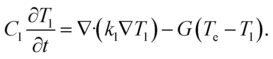
Femtosecond laser irradiation induced considerably less damage to the PET substrate than nanosecond laser irradiation (Fig. 7). Fig. 7a shows that femtosecond laser irradiation does not change the transmittance and roughness of the bare PET substrate at fluences where the nanowelding process and even the breakup of the NW network (F ≤ 200 mJ cm−2) occurred. The ablation of PET and severe surface modification occurred at F = 300 mJ cm−2, which is consistent with the result by Kumagai et al.35 On the other hand, the KrF excimer nanosecond laser decreased the transmittance of PET (Fig. 7b). The damage to the substrate was confirmed by AFM images within a scan area (5 μm by 5 μm). The root mean square roughness (Rq) increased to 7.0 nm, and the transmittance slightly decreased compared to bare PET at F = 10 mJ cm−2. Holes with a depth of approximately 20 nm were generated. As the laser fluence was increased, Rq substantially increased and nanostructures were generated on the PET surface. This surface modification is consistent with the result of the previous research, which reported that the damage threshold of PET by the KrF excimer laser was 5 mJ cm−2.17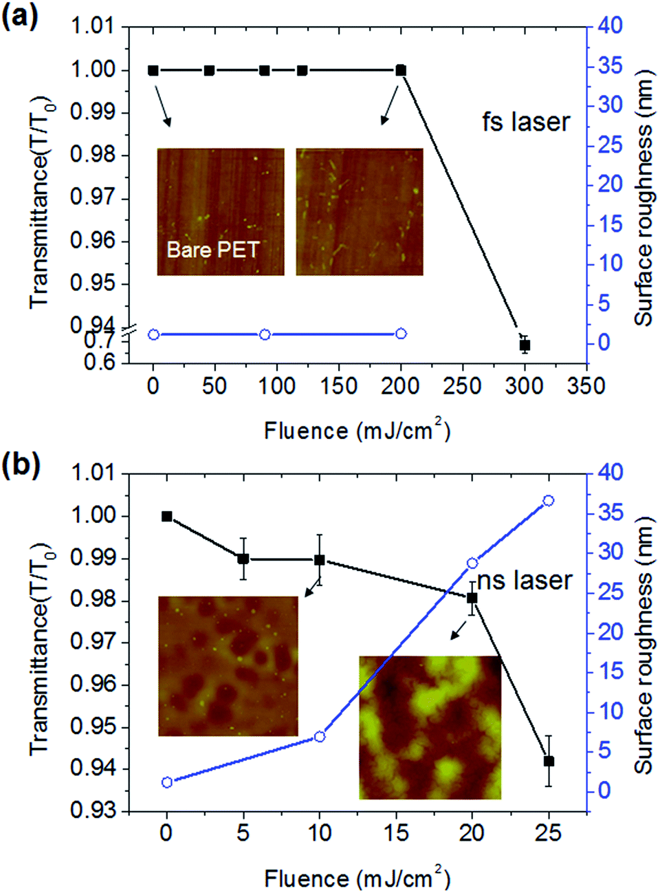 | ||
| Fig. 7 Transmittance normalized to the transmittance of bare PET (T/T0) and root mean square roughness (Rq) caused by (a) femtosecond laser irradiation and (b) nanosecond laser irradiation. The inlet images show the surface profile obtained using AFM. | ||
Non-thermal welding mechanism
Fig. 8a displays tiny nanoparticles (<5 nm) that were spread near the NWs after femtosecond laser irradiation while the mean diameter of the AgNWs decreased after laser treatment (Fig. 8b). The effective heat diffusion length of silver (>100 nm) after femtosecond laser irradiation is much larger than the diameter of the AgNWs (38 nm).36,37 Therefore, it is regarded that such a material ejection dominantly from the surface can be hardly caused by thermal explosion. We assume that the generation of tiny nanoparticles is attributed to non-thermal electron and ion emission caused by intense laser pulses. It has been reported that electrons and ions can be emitted from nanoparticles in highly intense laser fields of the order of 1012 W cm−2.38,39 The calculated intensity for current experimental condition (Fig. 5c) shows an enhanced value up to 2.8 × 10¹² W cm−2 at the gap of the AgNWs, supporting the possible electron and ion emission. Accompanied with electron and ion emission, possible scenario of the femtosecond laser-induced nanowelding process is briefly explained in the following. First, it has been proposed that electron emission can initiate decomposition of PVP layers and soften the lattice of the silver surface of silver nanoparticles.29 Similar softening of the AgNW lattice by electron emission can join adjacent AgNWs. Second, some portion of the material ejecta in the form of nanoparticles through ion emission process (confirmed by the formation of nanoparticles and decrease of wire diameter; refer to Fig. 8) can mediate the contact of the AgNWs. The nanoparticles generated at the hot spots easily adhere to the surface of the NWs to minimize the surface energy during the joining process.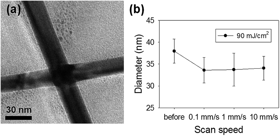 | ||
| Fig. 8 (a) TEM images shows the nanoparticles generated from the AgNW surfaces by femtosecond laser irradiation (F = 90 mJ cm−2, 0.1 mm s−1). (b) The diameter of silver NWs after laser irradiation for various scan speeds at F = 90 mJ cm−2. | ||
Comparison with nanosecond laser based nanowelding
To further confirm that the above-described joining characteristics were mainly due to an ultra-short time scale of energy deposition in femtosecond laser irradiation, similar experiments were repeated using a nanosecond laser. Recently, Nian et al.15 reported that controlled nanosecond laser irradiation (λ of 248 nm, τL of 25 ns) improves the NW cross junction conductance, and removes organic ligands. Fig. 9a and b show the sheet resistance and the transmittance of the AgNW films before and after excimer laser irradiation at various laser fluences, which is consistent with the results of the previous report. When 5 mJ cm−2 ≤ F ≤ 20 mJ cm−2, both sheet resistance and transmittance decreased with F increasing. At F = 25 mJ cm−2, the sheet resistance changed sharply to several MΩ. Fig. 9c shows the nanowelded junction of AgNWs caused by nanosecond laser irradiation at F = 20 mJ cm−2, where the sample showed the lowest sheet resistance. Nanosecond laser irradiation also generated nanoparticles as in the case of femtosecond laser irradiation. However, the particles were mostly aligned with the AgNWs (Fig. 9d), indicating that they were formed by thermal aggregation of molten NWs. At F = 25 mJ cm−2, molten AgNWs were converted into a chain of nanoparticles, which have the mean diameter of 130 nm ± 35 nm (Fig. 9d). Possibly, this transformation is a thermal phenomenon induced by the Rayleigh instability of molten NWs.40 | ||
| Fig. 9 (a) Sheet resistances and transmittances of the AgNW films before and after nanosecond laser irradiation at (a) various laser fluences (with a fixed pulse number of 100) and (b) pulse numbers. SEM images of AgNWs at (c) F = 20 mJ cm−2 and (d) F = 25 mJ cm−2. | ||
The AgNWs damaged by femtosecond laser irradiation have remarkable difference from those damaged by nanosecond laser irradiation (Fig. 10). In the case of femtosecond laser irradiation at F = 180 mJ cm−2, the breakup of the junction was observed. We observed tiny nanoparticles at the junction through laser irradiation possibly by the photofragmentation of AgNWs. The photofragmentation of nanoparticles can be explained by the two different mechanisms: the photothermal evaporation model and the Coulomb explosion model.41 In this work, the exact mechanism is not yet clear, and further studies on the mechanism of the fragmentation of silver NWs using femtosecond laser irradiation are needed. However, it is clearly observed that femtosecond laser irradiation can induce explosive fragmentation of NWs, which results in the formation of tiny nanoparticles (<10 nm) at the junctions, while nanosecond laser irradiation generates chains of relatively larger nanoparticles (>100 nm) formed by resolidification of melted atoms in the whole region.
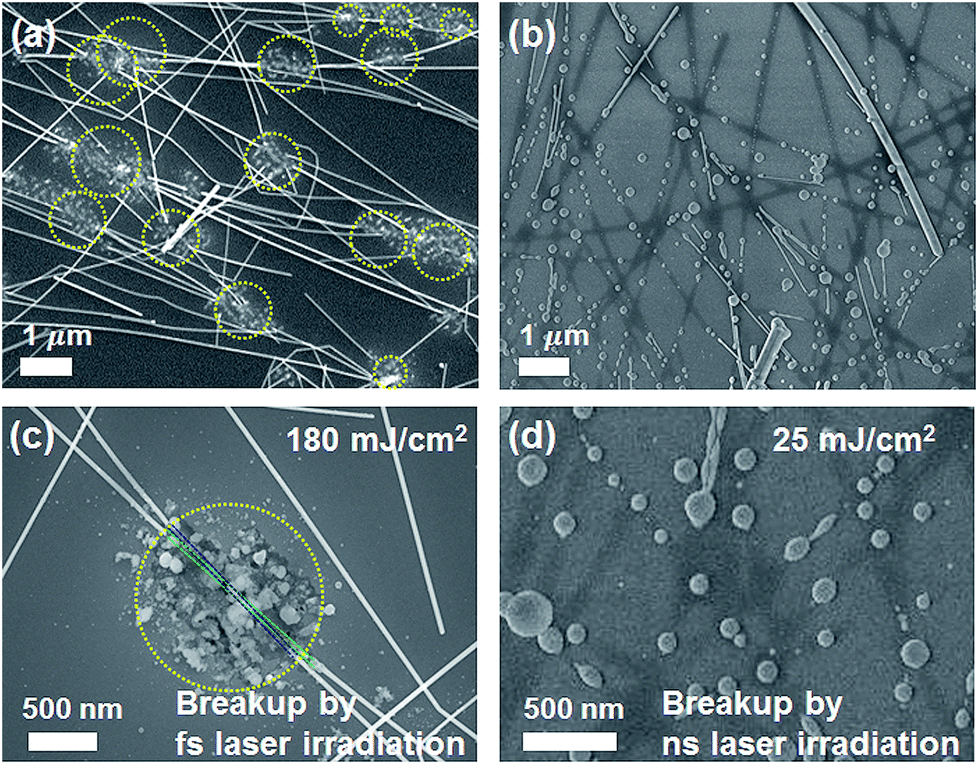 | ||
| Fig. 10 SEM images of the AgNW films broken up by (a and c) femtosecond laser irradiation at F = 180 mJ cm−2 and (b and d) nanosecond laser irradiation at F = 25 mJ cm−2. | ||
The different aspects of laser-induced damage on the AgNWs caused by femtosecond laser irradiation and nanosecond laser irradiation can also verify that femtosecond laser irradiation induces a smaller thermal side effect compared to nanosecond laser irradiation. Although heat generation is localized near the junction by the localized electric field between the gap of NWs, heat is diffused by electron–phonon and phonon–phonon coupling across and along the NWs. The thermal penetration depth was calculated to be approximately 360 nm upon femtosecond laser irradiation assisted by electron diffusion and electron–phonon coupling, whereas the thermal penetration depth caused by nanosecond laser irradiation (τL = 25 ns) was calculated to be 2.5 μm. We observed that the damage region of silver NW was localized within several hundred nanometers from the junction in the case of femtosecond laser irradiation (Fig. 10a and c). On the other hand, in the case of nanosecond laser irradiation, heat is diffused along the whole NW, which leads to melting the whole NW and the transformation into series of nanospheres all over the region (Fig. 10b and d).
Conclusions
In this work, we report a method for nanowelding AgNWs using femtosecond laser irradiation. Both sheet resistance and transmittance of the AgNW network were improved up to 25 Ω sq−1 and 94.3% at 633 nm, respectively. Femtosecond laser irradiation allowed joining of atoms strictly near the junction maintaining original crystallinity and shape of each AgNW, which was confirmed by TEM analyses. We propose possible joining mechanisms based on electron emission upon high-intensity femtosecond laser irradiation (>1012 W cm−2). In addition, we showed that femtosecond laser irradiation could induce highly localized heating process by observing the localized damage (<500 nm from the junction) without thermal aggregation and transformation into a chain of nanospheres. The femtosecond laser nanowelding process was free from damage on the underlying PET substrate, indicating its potential to the fabrication of transparent conducting electrodes and integrated plasmonic devices on temperature sensitive flexible substrates.Acknowledgements
This work was supported by the NRF Basic Research Programs (2014R1A2A1A11049453) and by the Korean Ministry of Trade, Industry and Energy (10048726).Notes and references
- L. B. Hu, H. S. Kim, J. Y. Lee, P. Peumans and Y. Cui, ACS Nano, 2010, 4, 2955–2963 CrossRef CAS PubMed.
- V. Scardaci, R. Coull, P. E. Lyons, D. Rickard and J. N. Coleman, Small, 2011, 7, 2621–2628 CrossRef CAS PubMed.
- J. Y. Lee, S. T. Connor, Y. Cui and P. Peumans, Nano Lett., 2008, 8, 689–692 CrossRef CAS PubMed.
- S. Coskun, E. S. Ates and H. E. Unalan, Nanotechnology, 2013, 24, 125202–125209 CrossRef PubMed.
- H. H. Khaligh and I. A. Goldthorpe, Nanoscale Res. Lett., 2013, 8, 235–240 CrossRef PubMed.
- J. O. Zhao, H. Y. Sun, S. Dai, Y. Wang and J. Zhu, Nano Lett., 2011, 11, 4647–4651 CrossRef CAS PubMed.
- D. P. Langley, M. Lagrange, G. Giusti, C. Jimenez, Y. Brechet, N. D. Nguyen and D. Bellet, Nanoscale, 2014, 6, 13535–13543 RSC.
- T. Tokuno, M. Nogi, M. Karakawa, J. T. Jiu, T. T. Nge, Y. Aso and K. Suganuma, Nano Res., 2011, 4, 1215–1222 CrossRef CAS.
- T.-B. Song, Y. Chen, C.-H. Chung, Y. Yang, B. Bob, H.-S. Duan, G. Li, K.-N. Tu, Y. Huang and Y. Yang, ACS Nano, 2014, 8, 2804–2811 CrossRef CAS PubMed.
- A. Vafaei, A. M. Hu and I. A. Goldthorpe, Nano-Micro Lett., 2014, 6, 293–300 CrossRef.
- E. C. Garnett, W. S. Cai, J. J. Cha, F. Mahmood, S. T. Connor, M. G. Christoforo, Y. Cui, M. D. McGehee and M. L. Brongersma, Nat. Mater., 2012, 11, 241–249 CrossRef CAS PubMed.
- J. Jiu, M. Nogi, T. Sugahara, T. Tokuno, T. Araki, N. Komoda, K. Suganuma, H. Uchida and K. Shinozaki, J. Mater. Chem., 2012, 22, 23561–23567 RSC.
- J. Jiu, T. Sugahara, M. Nogi, T. Araki, K. Suganuma, H. Uchida and K. Shinozaki, Nanoscale, 2013, 5, 11820–11828 RSC.
- J. A. Spechler and C. B. Arnold, Appl. Phys. A: Mater. Sci. Process., 2012, 108, 25–28 CrossRef CAS.
- Q. Nian, M. Saei, Y. Xu, G. Sabyasachi, B. Deng, Y. P. Chen and G. J. Cheng, ACS Nano, 2015, 9, 10018–10031 CrossRef CAS PubMed.
- J. A. Spechler, K. A. Nagamatsu, J. C. Sturm and C. B. Arnold, ACS Appl. Mater. Interfaces, 2015, 7, 10556–10562 CAS.
- D. Dunn and A. Ouderkirk, Macromolecules, 1990, 23, 770–774 CrossRef CAS.
- J. A. Sell, D. M. Heffelfinger, P. Ventzek and R. M. Gilgenbach, Appl. Phys. Lett., 1989, 55, 2435–2437 CrossRef CAS.
- U. Cristian, I. Bordianu, M. Dobromir, M. Drobota, C. Cotofana, M. Olaru and B. C. Simionescu, Rev. Roum. Chim., 2012, 57, 501–506 Search PubMed.
- U. Keller, Nature, 2003, 424, 831–838 CrossRef CAS PubMed.
- L. O. Herrmann, V. K. Valev, C. Tserkezis, J. S. Barnard, S. Kasera, O. A. Scherman, J. Aizpurua and J. J. Baumberg, Nat. Commun., 2014, 5, 4568 CAS.
- P. Lorazo, L. J. Lewis and M. Meunier, Phys. Rev. B: Condens. Matter Mater. Phys., 2006, 73, 134108 CrossRef.
- D. von der Linde and K. Sokolowski-Tinten, Appl. Surf. Sci., 2000, 154–155, 1–10 CrossRef CAS.
- G. Baffou and H. Rigneault, Phys. Rev. B: Condens. Matter Mater. Phys., 2011, 84, 035415 CrossRef.
- L. Liu, P. Peng, A. M. Hu, G. S. Zou, W. W. Duley and Y. N. Zhou, Appl. Phys. Lett., 2013, 102, 073107 CrossRef.
- H. Huang, M. Sivayoganathan, W. Duley and Y. Zhou, Appl. Surf. Sci., 2015, 331, 392–398 CrossRef CAS.
- S. Sundaram and E. Mazur, Nat. Mater., 2002, 1, 217–224 CrossRef CAS PubMed.
- J. Chen, W. K. Chen, J. Tang and P. M. Rentzepis, Proc. Natl. Acad. Sci. U. S. A., 2011, 108, 18887–18892 CrossRef CAS PubMed.
- H. Huang, L. Liu, P. Peng, A. Hu, W. W. Duley and Y. Zhou, J. Appl. Phys., 2012, 112, 123519 CrossRef.
- S. Inasawa, M. Sugiyama and Y. Yamaguchi, J. Phys. Chem. B, 2005, 109, 3104–3111 CrossRef CAS PubMed.
- E. D. Palik, Handbook of Optical Constants of Solids Part II, Academic, Orlando, Fla., 1985 Search PubMed.
- G. Chen, J. Heat Transfer, 1996, 118, 539–545 CrossRef CAS.
- Z. Cheng, L. Liu, S. Xu, M. Lu and X. Wang, Sci. Rep., 2015, 5, 10718 CrossRef CAS PubMed.
- A. Chimmalgi, C. Grigoropoulos and K. Komvopoulos, J. Appl. Phys., 2005, 97, 104319 CrossRef.
- H. Kumagai, K. Midorikawa, K. Toyoda, S. Nakamura, T. Okamoto and M. Obara, Appl. Phys. Lett., 1994, 65, 1850–1852 CrossRef CAS.
- A. M. Chen, H. F. Xu, Y. F. Jiang, L. Z. Sui, D. J. Ding, H. Liu and M. X. Jin, Appl. Surf. Sci., 2010, 257, 1678–1683 CrossRef CAS.
- A. P. Kanavin, I. V. Smetanin, V. A. Isakov, Y. V. Afanasiev, B. N. Chichkov, B. Wellegehausen, S. Nolte, C. Momma and A. Tünnermann, Phys. Rev. B: Condens. Matter Mater. Phys., 1998, 57, 14698–14703 CrossRef CAS.
- T. Döppner, T. Fennel, T. Diederich, J. Tiggesbäumker and K. H. Meiwes-Broer, Phys. Rev. Lett., 2005, 94, 013401 CrossRef PubMed.
- T. Döppner, T. Fennel, P. Radcliffe, J. Tiggesbäumker and K. H. Meiwes-Broer, Phys. Rev. A, 2006, 73, 031202 CrossRef.
- M. E. Toimil-Molares, A. G. Balogh, T. W. Cornelius, R. Neumann and C. Trautmann, Appl. Phys. Lett., 2004, 85, 5337–5339 CrossRef CAS.
- E. Akman, O. C. Aktas, B. G. Oztoprak, M. Gunes, E. Kacar, O. Gundogdu and A. Demir, Opt. Laser Technol., 2013, 49, 156–160 CrossRef CAS.
Footnote |
| † Electronic supplementary information (ESI) available. See DOI: 10.1039/c6ra19608j |
| This journal is © The Royal Society of Chemistry 2016 |