
Dioxin sensing properties of graphene and hexagonal boron nitride based van der Waals solids: a first-principles study†
M. Kamaraj,
J. Vijaya Sundar and
V. Subramanian*
Chemical Laboratory, CSIR – Central Leather Research Institute, Adyar, Chennai 600020, India. E-mail: subuchem@hotmail.com; subbu@clri.res.in; Fax: +91 44 24911589; Tel: +91 44 24411630
First published on 31st October 2016
Abstract
The changes in the electronic properties of single and bilayers of graphene (G) and hexagonal boron nitride (h-BN) two dimensional (2D) sheets have been investigated upon interaction with 2,3,7,8-tetrachlorodibenzo-p-dioxin (TCDD) by employing density functional theory (DFT) based calculations. The calculated interaction energy, band gap and charge transfer reveal that bilayer h-BN (BLBN) may serve as a better potential candidate for sensing TCDD than the other systems. To gain further insight into the sensing properties of these materials, the transmission spectra and current–voltage (I–V) characteristics have been calculated by using Non-Equilibrium Green's Function (NEGF) combined with DFT approach. It is interesting to mention that a Negative Differential Resistance (NDR) effect has been observed in a single layer BN (SLBN) nanoribbon upon interaction with TCDD. The calculated I–V characteristics of the BLBN nanoribbon–TCDD complex reveal that the interaction between the two systems enhances the current flow through the BLBN nanoribbon, which is appreciably higher than that of pristine BLBN. These findings may open up new avenues for the application of bilayers as possible sensors for pollutants.
1. Introduction
Graphene (G) is a perfect two-dimensional (2D) carbon system with zero band gap. It is one of the most fascinating materials of current century. Numerous studies have been carried out on this system due to its unique properties such as high carrier mobility,1 quantum Hall effect,2 high thermal conductivity and excellent optical transparency3 etc. Hexagonal boron nitride (h-BN) is an isostructural form of G, which is called ‘white graphene’. It is a wide band gap semiconductor. The stacking of these 2D materials has attracted the attention of researchers due to their tunable electronic and optoelectronic properties. The advances in the synthesis of atomically thin layers of van der Waals (vdW) bonded solids have opened new possibilities for the investigation of 2D systems. Several experimental studies have been made to synthesize G and h-BN using various techniques.4–6 The large-scale production of G4 and h-BN5,6 can be achieved by the chemical vapour deposition (CVD) method. The stacked homo and hetero bilayers of G and h-BN have also been synthesised using the same method.7–10 The CVD method facilitates the successful fabrication of graphene–hexagonal boron nitride (GBN) stacked layers.11–13 These fascinating stacked homo and hetero bilayers of 2D materials are referred as vdW solids. These have several applications in a variety of fields.14–16 It is well known from the previous investigations that G can be used (i) as a chemical and bio-molecular sensor,17–20 (ii) for DNA sequencing,21 and (iii) as an energy storage materials22 etc. The potential applications of graphene and N-doped graphene in catalysis have also been probed.23,24 Graphene oxide also used as sensor to detect bisphenol A.25 Similarly, the sensing property of h-BN has been investigated by using both experimental and theoretical techniques.26–33 The activated boron nitride has also been used to adsorb the organic pollutants.34 Lei et al. reported the importance of h-BN in the purification of water.35 Electronic properties of hBN have been tuned by various functionalization.36,37 The applications of hetero bilayers of G and h-BN as a possible pressure sensor38 and gas sensor39 have also been reported.Dioxin families are the most toxic organic pollutants. They are stable pollutants in water, soil, and air.40 It is lipophilic in nature.41 Dioxins are released during many industrial processes as an unwanted by-product. In some natural process such as volcanic eruptions and forest fire, dioxins are released.42 Any source of organic materials in the presence of chlorine or other halogens can generate dioxins and furans during combustion.41 The half-life of dioxin in soil and sediments is estimated to be 50–100 years.43 Among the members of dioxin family, 2,3,7,8-tetrachlorodibenzo-p-dioxin (TCDD) is highly toxic due to its half-life (10 years) in the human body.44,45 TCDD is a well-known carcinogen. The exposure of TCDD leads to skin problem called chloracne. Also, it affects the immune system and causes severe reproductive and developmental problems. Therefore, various experimental and theoretical studies have been carried out to sense TCDD with the help of new functional materials. Various nano materials are widely used in sensing of TCDD. Some of the significant studies on this topic are covered in the following section.
Single wall carbon nanotube (SWCNT) has been used as an efficient material for the removal of dioxin from waste incinerators.46 By using first principle calculation Fagan et al. showed that creation of lattice defect on SWCNT can increase the interaction of TCDD when compared to pristine SWCNT. The calculated interaction energy of the complex is −1.21 eV.47 The interaction of CNT and BNNT with TCDD has been investigated and it is found that TCDD interacts strongly with BNNT than CNT.48 The calculated interaction energy of TCDD with BNNT is −0.55 eV. Metal-doped graphene also been used as an effective adsorbent for TCDD.49,50 Ti doped graphene sheet shows interaction energy of −1.94 eV for TCDD and Ca decorated graphene has interaction energy of −3.20 eV. The dissociative interaction of dioxin on various metal oxide surfaces has also been studied and results suggested that the surface oxygen atoms of metal oxides with more nucleophilic character and less tightly bonded atoms might be promising sites for the decomposition of the dioxins and dibenzofurans.51
Experimentally, the sensing of environmental pollutants is a challenging task because of its high toxicity. Hence, computational chemistry approaches have been utilized to predict and design possible materials for the development of sensors. The specific surface to volume ratio of the nanomaterial is an important parameter in determining the sensitivity of the sensors. This value is much higher for nanomaterials based sensors than conventional micro sensors. Particularly, the 2D material provides the large adsorption area for sensing molecules as all of their atoms are exposed to the adsorbing molecules. Thus, highest sensing efficiency per unit volume can be achieved.21 The simple mechanism of the nanomaterial-based sensor is to detect the changes in the conductivity of material upon adsorption of analyte molecules. The changes in the conductivity could be attributed to the variations in the charge carrier concentration in the material as induced by adsorbed target molecules.
Since, G is a semimetal with zero band gap, and h-BN is wide band gap insulator, it is interesting to unravel the changes in the electronic properties of these materials upon surface interaction with TCDD. In this investigation, the following points have been addressed by using DFT based calculations combined with NEGF formalism.
(1) To understand the nature of interaction and binding modes of TCDD with G and h-BN single and their bilayers.
(2) To unravel the changes in the electronic structure, transport properties and I–V characteristics of G and h-BN single and their bilayer after interaction with TCDD.
(3) To predict a suitable material for sensing of TCDD based on the binding energy as well as the transport properties of single and bilayers of G and h-BN.
2. Theoretical models and method
In this study, the geometry optimization and electronic structure calculations were carried out by using the DFT method by employing the plane-wave pseudopotential formalism, as implemented in the Quantum ESPRESSO package.52 The local density approximation (LDA) with Perdew–Zunger (PZ)53 was used as an exchange correlation functional, and the core electrons were described by the ultrasoft pseudopotentials.54 The plane waves were expanded with a kinetic energy cutoff of 50 Ry. The convergence criteria for energy in SCF cycles was chosen to be 10−6 Ry, and the residual force on every atom was set to be less than 0.002 Ry bohr−1. The Monkhorst–Pack scheme55 of grid size 8 × 8 × 1 was used for the integration of electronic states. A vacuum spacing of 12 Å was introduced along non-periodic direction to minimize the spurious interactions between periodic supercell images. For the accurate calculation of the density of states (DOS), the tetrahedron method with 16 × 16 × 1 k-point mesh was used. The standard LDA and GGA functional failed to describe the vdW interactions. In order to include the vdW interactions, Lee et al. proposed the second version of the van der Waals density functional (vdW-DF2) which was employed in this investigation.56The transport properties were calculated using TransSIESTA code57 as implemented in SIESTA package.58 The computational details are presented in the ESI 1.† The LDA-DFT was previously used to obtain reliable results on lattice constants and binding energy of bilayers of G and h-BN systems.59,60 The same method was also yielded other electronic properties of these 2D systems in close agreement with the experimental results.61–64 The LDA-DFT method mimics features of the electronic band structure obtained by many-electron Green's function approach within the GW approximation reasonably well.65 LDA functional shows promising performance for noncovalent interactions between nanomaterials with various molecules.30,61–68 The choice of the LDA is not fortuitous and is more suitable than the GGA to study weakly interacting systems like the π-stacking interaction on sp2-like materials.69 It has been widely applied in the computational study of adsorption of the molecules on graphene and h-BN. Previous reports61–68 has also highlighted the accuracy of LDA functional. It should be worth to point out that the LDA-DFT method has been shown to provide reasonable good descriptions of the physics and chemistry of graphitic and hBN systems.61,62 Based on these solid reports, we have selected this functional in the present investigation.
As a benchmark, the geometrical and electronic properties of single layer graphene (SLG) (98C) and single layer of h-BN (SLBN) (49 B and 49 N) was calculated using 7 × 7 × 1 hexagonal supercell. The size of the supercell was chosen to keep the distance between TCDD molecules large enough to eliminate their interactions with neighbouring supercells. The supercell was constructed from the optimized unit cell with lattice constant of 2.44 Å for SLG and 2.48 Å for SLBN. The calculated C–C and B–N bond lengths are 1.41 and 1.45 Å, respectively. The calculated lattice constants (SLG – 2.44 Å, SLBN – 2.48 Å) and band gaps (SLG – 0 eV and SLBN – 4.39 eV) are consistent with previous results.70,71 Similarly, the bilayer graphene (BLG), bilayer h-BN (BLBN) and their hetero bilayers (GBN and BNG) were optimized. The calculated interlayer distances and band gap of these pristine homo and hetero bilayers are presented in ESI Table S1.† These values are also in good agreements with the previous reports.70,72,73
It has been found from previous studies13,73–76 that AB stacking arrangement in both homo and hetero bilayers was found to be the most stable one. The homo bilayer was constructed by placing the one G (h-BN) layer on the top of another G (h-BN) in the AB stacking arrangement. Similarly, the hetero bilayer system was constructed by stacking of G (h-BN) monolayer with the monolayer of h-BN (G). In this hetero bilayer arrangement, the carbon (boron) atom is on top of the boron (carbon) atom and the nitrogen atom is in the centre of hexagon of graphene. Thus, the AB stacking configuration was selected in this study for the construction of bilayers. The calculated mismatch in lattice constants between G and h-BN is less than 2%. The one-dimensional (1D) armchair nanoribbons were used for the calculation of transport properties (further details are included in ESI 2†).
The interaction energy (Eint) of TCDD adsorbed single and bilayers of G and h-BN were calculated by conventional definition Eint = Esub+ads − (Esub + Eads), where Eint, Esub+ads, Esub and Eads are interaction energy, total energy of the complexes, total energy of substrate and the total energy of adsorbate, respectively. The energetics of various binding modes of TCDD with single layer was calculated and it is found that AB stacking like pattern of TCDD is be the most stable arrangement. Hence, the same was chosen for the exploration of interaction of TCDD with bilayers.
3. Results and discussion
The optimized structure of isolated TCDD obtained from LDA level of theory is presented in Fig. 1. The optimized structural parameters are presented in Table 1 along with previous experimental data. The calculated bond lengths are in close agreement with the experimental values.77 Hence, the chosen level of theory is well suited for treating this molecule.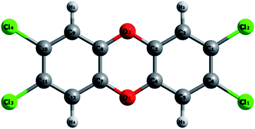 | ||
| Fig. 1 The optimized geometry of TCDD with LDA level of theory. | ||
| Atom | Bond lengths (Å) | |
|---|---|---|
| This work | Previous experimental work77 | |
| C2–H2 | 1.09 | — |
| C1–Cl2 | 1.70 | 1.72 |
| C1–C6 | 1.39 | 1.38 |
| C6–C5 | 1.37 | 1.38 |
| C5–C4 | 1.37 | 1.37 |
| C4–C3 | 1.39 | 1.38 |
| O2–C3 | 1.35 | 1.37 |
Both top and side view of the optimized geometries of all the complexes are shown in Fig. 2. It can be seen from Fig. 2(a) that the two aromatic rings of TCDD orient in AB stacking arrangement with reference to the basal plane of the graphene sheet. A similar kind of arrangement has also been observed to be the most stable one in the previous computational studies, where the aromatic molecules are stacked with graphene.78–80 Similarly, in the case of h-BN sheet, the carbon atoms (C1, C3, C5 and C8, C10, C12) in the aromatic ring of TCDD lie on the top of the boron atoms of sheet and the remaining three carbons lie at the centre of the hexagonal ring of the sheet as shown in Fig. 2(b).
 | ||
| Fig. 2 The top and side view of optimized geometry of TCDD on (a) SLG (b) SLBN (c) BLG (d) BLBN (e) GBN and (f) BNG. | ||
The calculated interaction energy (Eint), band gap (Eg), interlayer distance (dI) and optimized average vertical distance between the TCDD and the top layer of the sheet (dTCDD–sheet) are provided in Table 2. The calculated interaction energy values imply that TCDD forms stable complex with single and bilayers of G and h-BN. It can be seen from Table 2 that the optimized average vertical distance between the TCDD and the SLG is 3.27 Å. In the case of BLG, the average vertical distance between TCDD and the top layer of BLG is 3.24 Å. TCDD interacts strongly with the surface of BLG when compared to the interaction of TCDD with SLG. The calculated interaction energy of TCDD with SLG at LDA (vdW-DF2) level of theory is −0.75 (−1.25) eV. Upon inclusion of additional layer, the interaction energy increases. The interaction energy of TCDD with BLG at LDA (vdW-DF2) level of calculation is found to be −1.17 (−2.69) eV. A similar trend of increasing the interaction energy upon addition of another layer has already been observed in the interaction of benzene with multilayer graphene.81
| System | Eint (eV) | Eg (eV) | dI (Å) | dTCDD–sheet (Å) |
|---|---|---|---|---|
| a The values within the brackets was calculated with vdW-DF2 functional. | ||||
| SLG–TCDD | −0.75 (−1.25) | 0 | — | 3.27 (3.36) |
| BLG–TCDD | −1.17 (−2.69) | 0 | 3.33 (3.35) | 3.24 (3.26) |
| SLBN–TCDD | −0.91 (−1.89) | 3.12 | — | 3.08 (3.30) |
| BLBN–TCDD | −1.23 (−2.78) | 2.99 | 3.20 (3.21) | 3.06 (3.12) |
| GBN–TCDD | −0.84 (−1.83) | 0.06 | 3.19 (3.22) | 3.20 (3.18) |
| BNG–TCDD | −1.14 (−2.56) | 0.05 | 3.17 (3.19) | 3.13 (3.16) |
As expected, the weak vdW interaction plays the predominant role in the stabilization of the complexes. Hence, there is only a marginal change in the interlayer distance between two graphene sheets upon interaction with TCDD. The calculated band structures of SLG, SLG-TCDD and BLG-TCDD complexes are depicted in Fig. 3. The interaction of TCDD on both SLG and BLG does not significantly affect the electronic properties of graphene. The linear band near the Dirac point of pristine graphene survives after the interaction of TCDD on graphene. The presence of Dirac point and associated band structure clearly reveals that the stacking interaction does not alter the D6h symmetry of the graphene.
 | ||
| Fig. 3 Band structures of (a) pristine SLG, (b) SLG–TCDD and (c) BLG–TCDD. The Fermi level was set to be zero. | ||
The partial density of states (PDOS) of both SLG and BLG after interaction with TCDD is shown in Fig. 4. The highest occupied and lowest unoccupied states of TCDD hybridize with the G orbitals. As a result, some hybrid peaks are observed in PDOS of both SLG and BLG sheets. Overall findings reveal that the interaction of TCDD does not alter the electronic structure of graphene. However, significant increase in the interaction energy can be observed in the BLG when compared to SLG. Lowdin population analysis reveals that, significant amount of charge (electron) is transferred from TCDD to graphene systems. The calculated charge transfer from TCDD to BLG is 0.22e and for SLG–TCDD system is found to be is 0.09e. The increase in charge transfer may be responsible for the enhanced interaction of TCDD with BLG.
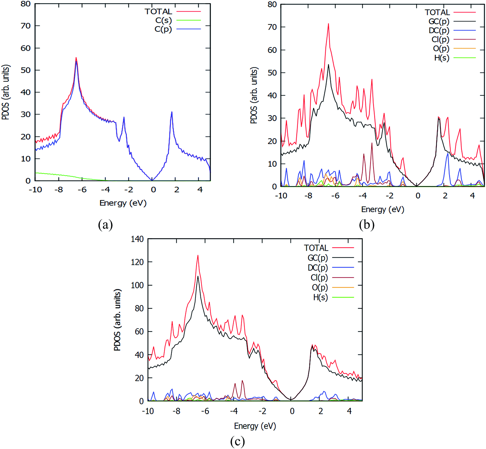 | ||
| Fig. 4 Partial density of states (PDOS) of (a) pristine SLG, (b) SLG–TCDD and (c) BLG–TCDD. The Fermi level was set to be zero. | ||
The optimized geometries of SLBN–TCDD and BLBN–TCDD are presented in Fig. 2(b) and (d). The calculated interaction energies at LDA (vdw-DF2) level of theory for SLBN–TCDD and BLBN–TCDD complexes are −0.91 (−1.89) eV and −1.23 (−2.78) eV, respectively. The trend in the interaction energy for these systems is similar to that of SLG–TCDD and BLG–TCDD complexes. However, the calculated interaction energy for BLBN–TCDD complex is relatively higher than that of BLG–TCDD complexes by about ∼1.38 kcal mol−1. The optimized average distances between TCDD and SLBN as well as BLBN are 3.08 and 3.06 Å, respectively. It can be seen from the Table 2 that, the interaction distance between TCDD with BLBN is less than all other systems implying the strong interaction between TCDD and BN layers.
The band structures of SLBN, SLBN–TCDD and BLBN–TCDD are given in Fig. 5. It is well known that SLBN is a wide band gap semiconductor with a value of 4.39 eV. It is possible to observe from Table 2 that band gap of SLBN reduces to 3.12 eV after interaction with TCDD. Similarly, in the case of BLBN, the band gap decreases after interaction with TCDD from 4.32 eV to 2.99 eV. The strong interaction of TCDD introduces new flat bands in the band gap region of both SLBN and BLBN. The reduction of bandgap may be due to the recombination of the energy levels of BN sheet with those of TCDD. This is also reinforced by the PDOS of SLBN and BLBN as shown in Fig. 6. The PDOS indicates that both valence band and conduction bands originate from C2p orbitals of TCDD. From the Lowdin charge analysis, it is found that 0.20e is transferred from TCDD to SLBN. However, the same from TCDD to BLBN is 0.42e. This may be the reason for the highest interaction energy in case of BLBN systems. Thus, the interaction of TCDD with these layers affect the conductivity of the both SLBN and BLBN and thus concomitant enhancement in the electronic response can be exploited for the development of sensors.
 | ||
| Fig. 5 Band structures of (a) pristine SLBN, (b) SLBN–TCDD and (c) BLBN–TCDD. The Fermi level was set to be zero. | ||
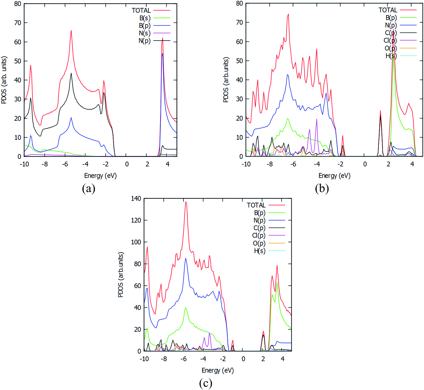 | ||
| Fig. 6 PDOS of (a) pristine SLBN, (b) SLBN–TCDD and (c) BLBN–TCDD. The Fermi level was set to be zero. | ||
The optimized structures of graphene–h-BN (GBN) and h-BN–graphene (BNG) with TCDD are presented in Fig. 2(e) and (f). The optimised distance between TCDD and GBN is found to be 3.20 Å. The same distance between TCDD and BNG is 3.13 Å. Among these hetero bilayers, the stronger interaction between TCDD with BNG is evident from these distances. The difference in the interaction energy of BNG–TCDD and GBN–TCDD complexes is about ∼6.92 kcal mol−1. The calculated band structures of GBN and BNG after interaction of TCDD are depicted in ESI Fig. S1.† The predicted bandgaps of both GBN and BNG bilayers are 0.063 and 0.053 eV, respectively. The interaction of TCDD does not influence band gap of hetero bilayers. The calculated charge transfers from TCDD to BNG as well as GBN are 0.31e and 0.25e, respectively. The calculated PDOS (ESI Fig. S2†) indicates that there are no changes near Fermi levels of both BNG and GBN after interaction with TCDD. Thus, electronic properties of these hetero bilayers remain unchanged after interaction of TCDD.
Results obtained from the calculation highlighted that BLBN–TCDD complex has higher interaction energy than rest of the complexes. Interaction energy is one of the important criteria to quantify the sensing ability of host materials. Among the six model (SLBN, SLG, BLG, BLBN, GBN and BNG) systems, BLBN nano sheet effectively sense TCDD. This stronger interaction allows adsorption of TCDD over BLBN for long time. It is well known that the parameter that determines the employment of these materials as a suitable substrate for sensing adsorbates is the recovery time.31 Hence a discussion on the recovery time has been qualitatively included in the following section.
The recovery time (τ) can be expressed by the conventional transition state theory31 as given below
| τ = ν0−1e(−Eint/κT) |
In general, the selectivity of guest molecules (H2, No, NH2, CH3, TTF, TCNQ, etc.) interacting over 2D materials can be easily monitored by measuring the output current of pristine and complex materials. The interaction of various target molecules on 2D h-BN system shows different band gap. For example, the interaction of TCNQ on BN sheet decreases the band gap of BN sheet to 0.43 eV, and TTF to 2.07 eV. Similarly, the interaction of O atom on BN sheet decreases the band gap of the BN systems to 3.8 eV. From molecular level calculations, the interaction of para-nitrophenol on the BN nanosheet decreases the band gap of BN nanosheet from 5.93 eV to 3.85 eV.32 So interaction of different target molecules shows different values of band gap, so obviously the conductivity of these systems are different from TCDD interacting systems. In the present investigation, we highlighted that the adsorption of TCDD decreases the band gaps of BLBN and SLBN to 2.9 eV and 3.1 eV, these changes in the band gap will increase the electrical conductivity. Results reveal that, the interaction of TCDD over BLBN reduces the band gap of the sheet from 4.3 eV to 2.9 eV. Therefore, the electrical conductivity of the BLBN sheet increases. We have measured the output current of BLBN sheet before and after interaction of TCDD complex. It was pictorially represented in Section 5. So selectivity of TCDD can be monitored by measuring the output currents before and after interaction. It is found from previous report36 that, the small changes in the band gap of Al-doped BN sheet, influences the large different in electrical conductivity of the material.
4. Zero bias transmission
A quantitative investigation of the transport properties of TCDD interacted single and bilayers (homo and hetero) of G and h-BN armchair nanoribbon has been undertaken. The model system consists of two semi-infinite right and left electrode regions in contact with the scattering regions as shown in a Fig. 7. The relaxed geometries of all the nanoribbons with TCDD are presented in ESI Fig. S3.† The same nomenclature in the case of 2D sheets is adopted. | ||
| Fig. 7 Schematic representation of electrode and scattering region of model systems. | ||
Both transmission spectra and DOS for SLG nanoribbon before and after interaction with TCDD at zero bias are represented in Fig. 8. The step-like behaviour in transmission spectra is observed due to the conductance channels in the band structure. The interaction of TCDD with SLG nanoribbon leads to the appearance of dips in the transmission spectra. These are also in accordance with the DOS that contains a localized peak at −0.8 eV below the Fermi level. It can be noticed from Fig. 8 that the interaction of TCDD causes a decrease in the conductance of SLG nanoribbon. The decrease in the conduction can be attributed to the electronic perturbation in the nanoribbon after interaction of TCDD. This perturbation may lead to intrinsic backscattering along the sheet, which alters conduction manifolds and reduces the transmission capability of the system.84 The computed transmission spectra and DOS of BLG nanoribbon before and after interaction with TCDD are shown in Fig. 9. The step-like behaviour is maintained after interaction of TCDD in BLG nanoribbon with a small localized peak at −0.85 eV. The zero bias transmission spectra and DOS of SLBN nanoribbon before and after interaction of TCDD are depicted in Fig. 10. The disappearance of step-like behaviour can be noticed after interaction with TCDD. As observed from ESI Table S2,† pristine SLBN nanoribbon is a wide gap semiconductor with a band gap of 4.55 eV. After interaction of TCDD the band gap decreases to 3.14 eV. The reduction in band gap is reflected in transmission spectra and DOS. As evident from DOS, peak is observed at 1.82 eV above the Fermi level. Similarly, in case of BLBN nanoribbon, the band gap decreases from 4.34 eV to 3.02 eV after interaction with TCDD. The computed zero bias transmission spectra and DOS of BLBN nanoribbon are displayed in Fig. 11. It is clearly evident from Fig. 11(a) that, after interaction of TCDD on BLBN nanoribbon a localized peak can be found at −1.30 eV below the Fermi level. Above Fermi level, another peak can be seen at 2.43 eV. The interaction of TCDD is responsible for the increase in the conductance of bilayer BN system. The zero bias transmission spectra of hetero bilayers (both GBN and BNG) nanoribbons before and after interaction with TCDD are given in ESI Fig. S4(a) and S5(a).† The step-like behaviour is observed in both cases. However, in the case of GBN system, there are no appreciable changes in the transmission spectra near Fermi level before and after interaction of TCDD. In the case of BNG systems, considerable variations in the transmission spectra can be seen at −0.75 eV below the Fermi level which arises due to the interaction of TCDD. The zero bias DOS of both the hetero bilayers are presented in ESI Fig. S4(b) and S5(b).†
 | ||
| Fig. 8 Zero bias transmission spectra (a) and DOS (b) of SLG nanoribbon before and after interaction with TCDD. | ||
 | ||
| Fig. 9 Zero bias transmission spectra (a) and DOS (b) of BLG nanoribbon before and after interaction with TCDD. | ||
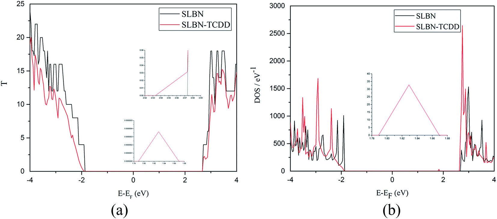 | ||
| Fig. 10 Zero bias transmission spectra (a) and DOS (b) of SLBN nanoribbon before and after interaction with TCDD. | ||
 | ||
| Fig. 11 Zero bias transmission spectra (a) and DOS (b) of BLBN nanoribbon before and after interaction with TCDD. | ||
5. I–V characteristics
The calculation of current–voltage (I–V) characteristics helps to quantitatively predict the feasibility of material as a sensor to recognize molecules. The I–V characteristics of G and BN nanoribbons and their bilayers were studied before and after interaction with TCDD. The information obtained from the I–V studies can through light on the realistic changes in the conductance of nanoribbon which is caused by the electronic perturbation of TCDD. It is well known that the electronic devices always work under a finite bias voltage. Hence, it is important to study the transport properties under the wide range of input bias voltage (Vb). In present calculation, Vb was varied from 0.0 to 3.0 V (up to 4 V in case of SLBN and BLBN nanoribbons) in steps of 0.2 V.The current as a function of applied voltage of SLG–TCDD nanoribbon complex is shown in Fig. 12(a). The current flow through SLG–TCDD nanoribbon is slightly less than that of SLG. The interaction of TCDD decreases the conductivity of SLG nanoribbon which is in good agreement with the calculated transmission spectra and DOS. The same trend is observed after interaction of TCDD with BLG as presented in Fig. 12(b). Interestingly, the conductivity of SLBN nanoribbon after interaction with TCDD increases the flow of current when the input bias voltage is 3.0 V. The Negative Differential Resistance (NDR) effect has been observed in the SLBN after interaction with TCDD as shown in Fig. 13(a). The NDR effect is an important quantum transport phenomenon. It is very useful in many device applications like analog to digital conversions, amplifications, noise rectifications, etc. The NDR effect is a nonlinear changes in the current with respect to an applied bias voltage. The origin of the observed NDR effect may be related to the changes in the transmission spectra and the DOS with different input bias voltage.
 | ||
| Fig. 12 The current–voltage (I–V) characteristics of pristine and TCDD adsorbed (a) SLG (b) BLG. | ||
 | ||
| Fig. 13 The current–voltage (I–V) characteristics of pristine and TCDD adsorbed (a) SLBN (b) BLBN. | ||
The DOS for the SLBN–TCDD (at Vb = 3.8 V) nanoribbon is shown in Fig. 14(a). The peaks are observed in the bias window due to the interaction of TCDD with SLBN nanoribbon which facilitates the tunneling of electron that leads to sharp increase in the current. When Vb is equal to 4.0 V, the reduction in the degree of tunneling occurs due to the absence of such peaks in the bias window. Thus, the decrease in the current with increase in Vb is observed (Fig. 14(b)). This NDR effect has already been observed in fluorinated BNNR, CNT, GNR and porous graphene.85–87
 | ||
| Fig. 14 The DOS of SLBN before and after interaction with TCDD at input bias voltage of (a) 3.8 V and (b) 4.0 V. The dashed line represents the bias window. | ||
The I–V characteristics of BLBN nanoribbon is shown in Fig. 13(b). In the bias voltage range from 0 to 2.8 V, the output current is zero. When Vb reaches to 2.8 V, an increase in the flow of current can be observed for the BLBN–TCDD nanoribbon systems. Further increasing the Vb, the flow of current also increases. The interaction of TCDD increases the flow of current. Hence, the interaction of TCDD with BLBN nanoribbon enhances the tunneling of electrons and as a result, significant increase in the current is observed. Thus, these variations are useful to detect or monitor the presence of TCDD. The I–V characteristics of hetero bilayers of GBN and BNG before and after interaction with TCDD are depicted in ESI Fig. S6(a) and (b).† It is evident from these figures that there are no noticeable changes in the I–V characteristics of these systems before and after interaction of TCDD.
6. Conclusions
In summary, the electronic and transport properties of the single and bilayers (homo and hetero) of G and h-BN sheets have been investigated before and after interaction with TCDD using density functional theory and NEGF based calculations. The interaction energy increases with the addition of another layer (i.e. single layer to bilayers). The order of interaction energy varies as BLBN > BLG > BNG > SLBN > GBN > SLG. Based on the findings from interaction energy calculations, the BLBN is a suitable candidate for the development of sensors for TCDD. From the band structure analysis, significant reduction in band gap has been observed in the case of SLBN and BLBN. The band gap of SLBN decreases from 4.39 to 3.12 eV after interaction with TCDD. Similarly, the band gap of BLBN reduces to 2.99 eV after interaction with TCDD. This reduction in the band gap increases the conductivity of these systems. The Lowdin charge analysis clearly reveals the appreciable charge transfer from TCDD to BLBN. The transmission spectra calculation reveals the presence of NDR effect in the SLBN nanoribbon after interaction of TCDD. Significant enhancement in the conductivity of BLBN nanoribbon can also be found after the interaction with TCDD. Overall results from electronic and transport properties illustrate that BLBN systems are more suitable for sensing TCDD when compared to graphene counterparts.Acknowledgements
We acknowledge the Multi-Scale Simulation and Modeling project – MSM (CSC0129) funded by CSIR and Design and Development of Two-Dimensional van der Waals Solids funded by DST (No. EMR/2015/000447). We also acknowledge the high-performance computing center (CMMACS-4PI) Bangalore for providing additional computational facilities.References
- K. Novoselov, A. K. Geim, S. Morozov, D. Jiang, M. Katsnelson, I. Grigorieva, S. Dubonos and A. Firsov, Nature, 2005, 438, 197–200 CrossRef CAS PubMed.
- X. Du, I. Skachko, A. Barker and E. Y. Andrei, Nat. Nanotechnol., 2008, 3, 491–495 CrossRef CAS PubMed.
- R. Nair, P. Blake, A. Grigorenko, K. Novoselov, T. Booth, T. Stauber, N. Peres and A. Geim, Science, 2008, 320, 1308 CrossRef CAS PubMed.
- X. Li, W. Cai, J. An, S. Kim, J. Nah, D. Yang, R. Piner, A. Velamakanni, I. Jung and E. Tutuc, Science, 2009, 324, 1312–1314 CrossRef CAS PubMed.
- L. Song, L. Ci, H. Lu, P. B. Sorokin, C. Jin, J. Ni, A. G. Kvashnin, D. G. Kvashnin, J. Lou and B. I. Yakobson, Nano Lett., 2010, 10, 3209–3215 CrossRef CAS PubMed.
- K. K. Kim, A. Hsu, X. Jia, S. M. Kim, Y. Shi, M. Hofmann, D. Nezich, J. F. Rodriguez-Nieva, M. Dresselhaus and T. Palacios, Nano Lett., 2011, 12, 161–166 CrossRef PubMed.
- W. Liu, H. Li, C. Xu, Y. Khatami and K. Banerjee, Carbon, 2011, 49, 4122–4130 CrossRef CAS.
- W. Liu, S. Kraemer, D. Sarkar, H. Li, P. M. Ajayan and K. Banerjee, Chem. Mater., 2013, 26, 907–915 CrossRef.
- Y. Gao, W. Ren, T. Ma, Z. Liu, Y. Zhang, W.-B. Liu, L.-P. Ma, X. Ma and H.-M. Cheng, ACS Nano, 2013, 7, 5199–5206 CrossRef CAS PubMed.
- Y. Shi, C. Hamsen, X. Jia, K. K. Kim, A. Reina, M. Hofmann, A. L. Hsu, K. Zhang, H. Li and Z.-Y. Juang, Nano Lett., 2010, 10, 4134–4139 CrossRef CAS PubMed.
- Z. Liu, L. Song, S. Zhao, J. Huang, L. Ma, J. Zhang, J. Lou and P. M. Ajayan, Nano Lett., 2011, 11, 2032–2037 CrossRef CAS PubMed.
- M. Yankowitz, J. Xue, D. Cormode, J. D. Sanchez-Yamagishi, K. Watanabe, T. Taniguchi, P. Jarillo-Herrero, P. Jacquod and B. J. LeRoy, Nat. Phys., 2012, 8, 382–386 CrossRef CAS.
- S. M. Kim, A. Hsu, P. Araujo, Y.-H. Lee, T. Palacios, M. Dresselhaus, J.-C. Idrobo, K. K. Kim and J. Kong, Nano Lett., 2013, 13, 933–941 CrossRef CAS PubMed.
- A. K. Geim and I. V. Grigorieva, Nature, 2013, 499, 419–425 CrossRef CAS PubMed.
- S. Z. Butler, S. M. Hollen, L. Cao, Y. Cui, J. A. Gupta, H. R. Gutiérrez, T. F. Heinz, S. S. Hong, J. Huang and A. F. Ismach, ACS Nano, 2013, 7, 2898–2926 CrossRef CAS PubMed.
- X. Zhong, R. G. Amorim, R. H. Scheicher, R. Pandey and S. P. Karna, Nanoscale, 2012, 4, 5490–5498 RSC.
- W. Yuan and G. Shi, J. Mater. Chem. A, 2013, 1, 10078–10091 CAS.
- K. R. Ratinac, W. Yang, S. P. Ringer and F. Braet, Environ. Sci. Technol., 2010, 44, 1167–1176 CrossRef CAS PubMed.
- F. Schedin, A. Geim, S. Morozov, E. Hill, P. Blake, M. Katsnelson and K. Novoselov, Nat. Mater., 2007, 6, 652–655 CrossRef CAS PubMed.
- K. Balamurugan and V. Subramanian, J. Phys. Chem. C, 2013, 117, 21217–21227 CAS.
- S. K. Min, W. Y. Kim, Y. Cho and K. S. Kim, Nat. Nanotechnol., 2011, 6, 162–165 CrossRef CAS PubMed.
- R. Raccichini, A. Varzi, S. Passerini and B. Scrosati, Nat. Mater., 2015, 14, 271–279 CrossRef CAS PubMed.
- C. Huang, C. Li and G. Shi, Energy Environ. Sci., 2012, 5, 8848–8868 CAS.
- V. S. Jeyaraj, M. Kamaraj and V. Subramanian, J. Phys. Chem. C, 2015, 119, 26438–26450 CAS.
- Y. Zhu, Y. Cai, L. Xu, L. Zheng, L. Wang, B. Qi and C. Xu, ACS Appl. Mater. Interfaces, 2015, 7, 7492–7496 CAS.
- S. Liu, B. Lu, Q. Zhao, J. Li, T. Gao, Y. Chen, Y. Zhang, Z. Liu, Z. Fan and F. Yang, Adv. Mater., 2013, 25, 4549–4554 CrossRef CAS PubMed.
- M. Sajjad and P. Feng, Mater. Res. Bull., 2014, 49, 35–38 CrossRef CAS.
- J. Li, R. Dahal, S. Majety, J. Lin and H. Jiang, Nucl. Instrum. Methods Phys. Res., Sect. A, 2011, 654, 417–420 CrossRef CAS.
- T. Arnold, J. E. Parker and P. Macdonald, J. Phys. Chem. C, 2012, 116, 10599–10606 CAS.
- Q. Lin, X. Zou, G. Zhou, R. Liu, J. Wu, J. Li and W. Duan, Phys. Chem. Chem. Phys., 2011, 13, 12225–12230 RSC.
- M. Samadizadeh, A. A. Peyghan and S. F. Rastegar, Chin. Chem. Lett., 2015, 26, 1042–1045 CrossRef CAS.
- A. A. Peyghan, M. Noei and S. Yourdkhani, Superlattices Microstruct., 2013, 59, 115–122 CrossRef CAS.
- S. Thomas, A. C. Rajan, M. R. Rezapour and K. S. Kim, J. Phys. Chem. C, 2014, 118, 10855–10858 CAS.
- J. Li, X. Xiao, X. Xu, J. Lin, Y. Huang, Y. Xue, P. Jin, J. Zou and C. Tang, Sci. Rep., 2013, 3, 3208 Search PubMed.
- W. Lei, D. Portehault, D. Liu, S. Qin and Y. Chen, Nat. Commun., 2013, 4, 1777 CrossRef PubMed.
- J. Beheshtian, H. Soleymanabadi, A. A. Peyghan and Z. Bagheri, Appl. Surf. Sci., 2013, 268, 436–441 CrossRef CAS.
- J.-x. Zhao, Y.-y. Yu, Y. Bai, B. Lu and B.-x. Wang, J. Mater. Chem., 2012, 22, 9343–9350 RSC.
- Y. Xu, Z. Guo, H. Chen, Y. Yuan, J. Lou, X. Lin, H. Gao, H. Chen and B. Yu, Appl. Phys. Lett., 2011, 99, 133109 CrossRef.
- Y. He, M. Tsutsui, S. Ryuzaki, K. Yokota, M. Taniguchi and T. Kawai, NPG Asia Mater., 2014, 6, e104 CrossRef CAS.
- X. Zhou, Y. Wei, Q. He, F. Boey, Q. Zhang and H. Zhang, Chem. Commun., 2010, 46, 6974–6976 RSC.
- R. Addink, B. Van Bavel, R. Visser, H. Wever, P. Slot and K. Olie, Chemosphere, 1990, 20, 1929–1934 CrossRef CAS.
- S. Manzetti, E. R. van der Spoel and D. van der Spoel, Chem. Res. Toxicol., 2014, 27, 713–737 CrossRef CAS PubMed.
- S. Sinkkonen and J. Paasivirta, Chemosphere, 2000, 40, 943–949 CrossRef CAS PubMed.
- J. P. Whitlock Jr, Chem. Res. Toxicol., 1993, 6, 754–763 CrossRef CAS.
- R. T. Yang, R. Q. Long, J. Padin, A. Takahashi and T. Takahashi, Ind. Eng. Chem. Res., 1999, 38, 2726–2731 CrossRef CAS.
- R. Q. Long and R. T. Yang, J. Am. Chem. Soc., 2001, 123, 2058–2059 CrossRef CAS PubMed.
- S. B. Fagan, E. Santos, A. Souza Filho, J. Mendes Filho and A. Fazzio, Chem. Phys. Lett., 2007, 437, 79–82 CrossRef CAS.
- M. D. Ganji, H. Alinezhad, E. Soleymani and M. Tajbakhsh, Phys. E, 2015, 67, 105–111 CrossRef.
- H. S. Kang, J. Am. Chem. Soc., 2005, 127, 9839–9843 CrossRef CAS PubMed.
- H. Zhang, W. He, X. Luo, X. Lin and X. Lu, J. Mol. Model., 2014, 20, 1–7 CrossRef PubMed.
- S. Zhao, X. Ma, Q. Pang, H. Sun and G. Wang, Phys. Chem. Chem. Phys., 2014, 16, 5553–5562 RSC.
- P. Giannozzi, S. Baroni, N. Bonini, M. Calandra, R. Car, C. Cavazzoni, D. Ceresoli, G. L. Chiarotti, M. Cococcioni and I. Dabo, J. Phys.: Condens. Matter, 2009, 21, 395502 CrossRef PubMed.
- J. P. Perdew and A. Zunger, Phys. Rev. B: Condens. Matter Mater. Phys., 1981, 23, 5048 CrossRef CAS.
- D. Vanderbilt, Phys. Rev. B: Condens. Matter Mater. Phys., 1990, 41, 7892 CrossRef.
- H. J. Monkhorst and J. D. Pack, Phys. Rev. B: Solid State, 1976, 13, 5188 CrossRef.
- K. Lee, É. D. Murray, L. Kong, B. I. Lundqvist and D. C. Langreth, Phys. Rev. B: Condens. Matter Mater. Phys., 2010, 82, 081101 CrossRef.
- M. Brandbyge, J.-L. Mozos, P. Ordejón, J. Taylor and K. Stokbro, Phys. Rev. B: Condens. Matter Mater. Phys., 2002, 65, 165401 CrossRef.
- J. M. Soler, E. Artacho, J. D. Gale, A. García, J. Junquera, P. Ordejón and D. Sánchez-Portal, J. Phys.: Condens. Matter, 2002, 14, 2745 CrossRef CAS.
- Y. Sakai, S. Saito and M. L. Cohen, Phys. Rev. B: Condens. Matter Mater. Phys., 2014, 89, 115424 CrossRef.
- M. Hu, Z. Yu, J. Yin, C. Zhang and L. Sun, Comput. Mater. Sci., 2012, 54, 165–169 CrossRef CAS.
- S. Trickey, F. Müller-Plathe, G. Diercksen and J. Boettger, Phys. Rev. B: Condens. Matter Mater. Phys., 1992, 45, 4460 CrossRef CAS.
- A. Marini, P. García-González and A. Rubio, Phys. Rev. Lett., 2006, 96, 136404 CrossRef PubMed.
- N. Ooi, A. Rairkar and J. B. Adams, Carbon, 2006, 44, 231–242 CrossRef CAS.
- M. Hasegawa and K. Nishidate, Phys. Rev. B: Condens. Matter Mater. Phys., 2004, 70, 205431 CrossRef.
- L. Yang, C.-H. Park, Y.-W. Son, M. L. Cohen and S. G. Louie, Phys. Rev. Lett., 2007, 99, 186801 CrossRef PubMed.
- Y. Lu, W. Chen, Y. Feng and P. He, J. Phys. Chem. B, 2008, 113, 2–5 CrossRef PubMed.
- X. Tian, J. Xu and X. Wang, J. Phys. Chem. B, 2010, 114, 11377–11381 CrossRef CAS PubMed.
- T. Cao, X. Zheng, L. Huang, P. Gong and Z. Zeng, J. Phys. Chem. C, 2014, 118, 10472–10480 CAS.
- F. Tournus and J.-C. Charlier, Phys. Rev. B: Condens. Matter Mater. Phys., 2005, 71, 165421 CrossRef.
- Y. Baskin and L. Meyer, Phys. Rev., 1955, 100, 544 CrossRef CAS.
- L. Liu, Y. Feng and Z. Shen, Phys. Rev. B: Condens. Matter Mater. Phys., 2003, 68, 104102 CrossRef.
- X. Chen, F. Tian, C. Persson, W. Duan and N.-x. Chen, Sci. Rep., 2013, 3, 3046 Search PubMed.
- X. Zhong, Y. K. Yap, R. Pandey and S. P. Karna, Phys. Rev. B: Condens. Matter Mater. Phys., 2011, 83, 193403 CrossRef.
- K. Lee, S. Kim, M. Points, T. Beechem, T. Ohta and E. Tutuc, Nano Lett., 2011, 11, 3624–3628 CrossRef CAS PubMed.
- G. Gao, W. Gao, E. Cannuccia, J. Taha-Tijerina, L. Balicas, A. Mathkar, T. Narayanan, Z. Liu, B. K. Gupta and J. Peng, Nano Lett., 2012, 12, 3518–3525 CrossRef CAS PubMed.
- G. Constantinescu, A. Kuc and T. Heine, Phys. Rev. Lett., 2013, 111, 036104 CrossRef PubMed.
- A. W. Cordes and C. K. Fair, Acta Crystallogr., Sect. B: Struct. Sci., 1974, 30, 1621 CrossRef.
- A. AlZahrani, Appl. Surf. Sci., 2010, 257, 807–810 CrossRef CAS.
- J. Lee, K.-A. Min, S. Hong and G. Kim, Chem. Phys. Lett., 2015, 618, 57–62 CrossRef CAS.
- C.-H. Chang, X. Fan, L.-J. Li and J.-L. Kuo, J. Phys. Chem. C, 2012, 116, 13788–13794 CAS.
- S. Wangmo, R. Song, L. Wang, W. Jin, D. Ding, Z. Wang and R.-Q. Zhang, J. Mater. Chem., 2012, 22, 23380–23386 RSC.
- F. Chambers, G. Zajac and T. Fleisch, J. Vac. Sci. Technol., B: Microelectron. Process. Phenom., 1986, 4, 1310–1315 CAS.
- R. A. Wolfson, L. M. Arnold, P. Shrestha and A. D. Migone, Langmuir, 1996, 12, 2868–2871 CrossRef CAS.
- K. Z. Milowska and J. A. Majewski, J. Phys. Chem. C, 2014, 118, 17395–17401 CAS.
- J. Zeng, K.-Q. Chen and C. Q. Sun, Phys. Chem. Chem. Phys., 2012, 14, 8032–8037 RSC.
- M. Rinkio, A. Johansson, V. Kotimäki and P. Törmä, ACS Nano, 2010, 4, 3356–3362 CrossRef CAS PubMed.
- T.-T. Wu, X.-F. Wang, M.-X. Zhai, H. Liu, L. Zhou and Y.-J. Jiang, Appl. Phys. Lett., 2012, 100, 052112 CrossRef.
Footnote |
| † Electronic supplementary information (ESI) available. See DOI: 10.1039/c6ra18976h |
| This journal is © The Royal Society of Chemistry 2016 |