Alaa Y. Faidab and
Nageh K. Allam*a
aEnergy Materials Laboratory (EML), School of Sciences and Engineering, The American University in Cairo, New Cairo 11835, Egypt. E-mail: nageh.allam@aucegypt.edu
bLaboratory of Nanotechnology Applications in Electronics and Electrical Engineering, Electronics Research Institute, Cairo, Egypt
First published on 19th August 2016
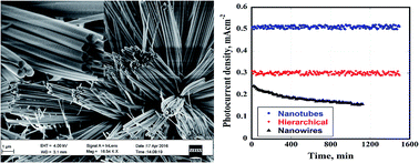
The development of high performance artificial photosynthetic devices, to store solar energy in chemical bonds, requires the existence of stable light-absorbing electrodes for both the oxidative and reductive half-reactions. The development of such systems has been hindered in part by the lack of semiconducting photoanodes that are stable under the water spitting conditions. We demonstrate, for the first time, the synthesis of ZnO nanotubes via anodization of Zn foil and their use as photoanodes in photoelectrochemical hydrogen generation systems. Structural, optical and photoelectrochemical measurements showed the superiority of the nanotubular structure over the nanowire and hierarchical counterparts.
Fig. 1 shows FESEM images of the fabricated nanostructures: well-aligned nanowires with diameters of 69 ± 5 nm, hierarchical nanowires with horn shaped ZnO crystals (nanoparticles decorated-nanowires), and hexagonal ZnO nanotubes with diameters of 130 ± 5 nm and average wall thickness of 20 ± 5 nm. More images can be seen in Fig. S1–S4 in the ESI.† During anodization, two competing processes resulted in the formation of ZnO nanostructures: the dissolution of zinc foil (Zn2+) and the simultaneous oxidation to ZnO. Tuning the anodization parameters allowed control of the two processes, leading to the presence or absence of nanostructures and, in the former case, control over their morphology and properties.
![]() | ||
Fig. 1 FESEM images of ZnO (a) nanowires, (b) hierarchical nanowires (nanoparticles decorated on nanowires), (c) top-view nanotubes, and (d) side-view nanotubes. |
The general reaction scheme for the anodization of zinc can be represented as follows:14
At the cathode: 2H+ + 2e− → H2(g) | (1) |
At the anode: Zn → Zn2+ + 2e− | (2) |
Zn2+ + 2OH− → Zn(OH)2 | (3) |
Zn(OH)2 → ZnO + H2O | (4) |
Dissolution: ZnO + HX* → ZnX* + H2O | (5) |
i = αeβF | (6) |
![]() | (7) |
![]() | (8) |
![]() | ||
Fig. 2 (a) Current–time response during the anodization of Zn foil to form ZnO nanostructures and (b) XRD pattern of the as-anodized and oxygen-annealed ZnO films. |
In the above equations e is the electron charge, k is Boltzmann's constant, T is the absolute temperature, a is one half of the jump distance, φ0 is the minimum potential barrier, and τ is the time of vibration. Note here that the charge associated with formation of a Zn2+ cation is ne where n = 2. The electric field linearly decreases with oxide layer thickness, while from eqn (6) the current will decay exponentially with film thickness.
The growth of the hierarchical nanowires was shown to occur via the branching of a single large, hexagonal wire into several smaller nanowires, with diameters similar to those at the start of the nanowire growth (Fig. S2†). These smaller nanowires, together with the underlying wires, continue to grow to form very thick nanowire films (>100 μm). As the thicknesses exceeds 50 μm, however, complex 3D networks of nanowires were typically formed rather than aligned nanowires,8 see ESI† for more details. Also, the two step anodization at 5 and 10 V resulted in nanowire/nanotube and nanotube morphologies, respectively (Fig. S3 and S4†). The exact reasons for both the formation of layered films of different sized nanowires and the formation of hierarchical structures are currently unknown. However, this could be related to the increasing distance from the source of Zn2+ ions to the nanowire tip, thereby reducing the concentration of Zn2+ ions available for reaction. It might also be attributed to a decreasing concentration of the already dilute bicarbonate species present in the electrolyte as a function of time.9 It is worthy to mention that leaving the nanowires film in a sealed vial containing deionized water for 24 h, followed by annealing for 1 h at 250 °C with heating and cooling rates of 1 °C min−1, resulted in the formation of hierarchical nanostructures. The soaking of ZnO nanowires in aqueous medium is thought to enrich the hydroxyl group content on the surface, which might facilitate the partial dissolution of Zn2+ ions and forms Zn(OH)2/[Zn(OH)4]2− and subsequently transforms to ZnO during the thermal treatment.
The co-existence of nanotubes and nanowires in the film indicate a unique mechanism for anodic nanotube growth. It does not appear fully consistent with the existing prominent models such as the stress-induced material flow for the anodic porous structure formation. To throw light into the nanotube formation mechanism, experiments were conducted on zinc foils anodized at different durations. The sample obtained after anodization for 10 s showed shallow etched pits from where needles started growing out. A sea urchin-like growth pattern appeared after 30 s. The needles were transformed into hexagonal rods of about 2 μm in one minute of anodization. At this time, pits started appearing on the flat top surface of the wire, which grew deeper with a concurrent increase in the nanowire length, resulting in more or less hexagonally shaped tubular structure. It was also obvious that a minimum diameter (∼100 nm) was required for the rods to have tubular conversion. A similar size effect was reported in single crystal zinc rods formed by other techniques when converted later to tubes by etching in acidic or alkaline media.
It can be concluded that anodization for short time at low potential leads to the formation of tubes, while increasing both time and potential resulted in the formation of nanowires. Table 1 summaries the fabrication conditions and the obtained morphologies.
Electrolyte composition | Voltage [V] | Time [min] | Post treatment | Obtained structure |
---|---|---|---|---|
50 mM KHCO3 | 10 | 30 | Annealing | Nanowires |
50 mM KHCO3 | 10 | 30 | Water treatment + annealing | Hierarchical |
50 mM KHCO3 | 10 then 5 | 30 then 10 | Annealing | Nanowires/nanotubes |
50 mM KHCO3 + 30 mM Na2CO3 | 10 | 10 | Annealing | Nanotubes |
X-ray diffraction (XRD) analysis was performed for as-anodized and oxygen-annealed samples to elucidate their crystal structure, Fig. 2b. The XRD pattern of the as-anodized nanotubes showed a complex set of sharp peaks that can be assigned to the metal zinc foil (JCPDS 04-0831), as well as several broad peaks corresponding to the hexagonal wurtzite ZnO (JCPDS 36-1451). Upon annealing, the intensity of the ZnO diffraction peaks associated with (100), (002), (101), (012), (110), (013), (200), and (202) lattice planes drastically increased, indicating the formation of polycrystalline wurtzite ZnO structures. Note that all tested morphologies showed similar diffraction patterns, with the nanotubes showing the most intense peaks.
The high resolution transmission electron microscopy (HRTEM) investigation, Fig. 3, further confirms the formation of polycrystalline one-dimensional ZnO nanotubes, which is consistent with the XRD results. The spotty ring in the selected area electron diffraction (SAED) pattern shows six diffraction rings corresponding to (100), (002), (102), (110), (103), and (112) lattice planes of ZnO. The lattice fringes spectra showed a spacing of 4.1 Å, characteristic of ZnO.
To elucidate the composition of the fabricated nanotubes, X-ray photoelectron spectroscopy (XPS) analysis was performed with the spectra charge referenced to O 1s at 532 eV, Fig. 4. The spectra showed well-resolved Zn 2p and O 1s peaks that are characteristic of ZnO. While the peak observed at 531 eV is characteristic of Zn–O bonding, the shoulder extending to 532.2 eV can be related to the O–H bonding. Doublet Zn peaks were observed at 1022.19 and 1045.14 eV, with a spin orbit splitting of ∼23 eV correspond to Zn2+.12–14,18
Raman-scattering is another effective technique to investigate the crystallinity and the vibrational properties of materials as the Raman signals are very sensitive to the crystal structure and defects. Wurtzite ZnO, which belongs to the P63mc space group, would possess six Raman active vibration modes:19
T = A1 + 2B1 + E1 + 2E2 | (9) |
Both A1 and E1 modes are polar and split into transverse optical (A1TO and E1TO) and longitudinal optical (A1LO and E1LO) components.20 B1 is silent and E2 has two modes of low and high frequency phonons (E2 low and E2 high), which are associated with the vibration of the Zn sub-lattice and oxygen atom.20 The peaks appeared at 208, 438 and 574 cm−1, Fig. 5a, can be assigned to the E2 low, E2 high and A1 LO, respectively.21 The Raman peak at 438 cm−1 may be attributed to the non-polar optical phonon mode of ZnO (E2 mode), characteristic of the hexagonal wurtzite phase.22 The peak at 578 cm−1 corresponds to the LO mode with A1 symmetry.22 Besides these first-order Raman modes, the E(LO) Raman peak can be assigned to the second-order Raman mode due to the vertical alignment of the nanotubes.23
![]() | ||
Fig. 5 (a) Raman spectra, (b) normalized absorption, (c) photoelectrochemical properties, and (d) the current transients of the fabricated ZnO nanostructures. |
Fig. 5b shows the typical UV-vis diffuse reflectance spectra (DRS) of the fabricated ZnO nanostructured materials.14 Note that all films showed similar absorption spectra with a small red shift in the absorption edge from nanowires (3.31 eV) to the hierarchical structure (3.23 eV), nanowires/nanotubes structure (3.2 eV) and the nanotubes (3.15 eV). The differences in the bandgaps are within experimental error and therefore can be attributed to scattering effects due to the different film morphologies.14
The photoelectrochemical activity test for water photoelectrolysis using the grown ZnO nanostructured films was carried out in a 0.5 M Na2SO4 electrolyte solution using a typical three-electrode electrochemical cell, where the annealed ZnO nanostructured film is used as the working electrode, Pt foil as the counter electrode, and calomel as the reference electrode connected to Biologic SP200 potentiostat. Previous reports showed that ZnO nanostructures undergo photocorrosion upon their use in water splitting cells, due to the formation of a precipitate on the surface that hinders their proper irradiation.24 Under AM 1.5G illumination (100 mW cm−2), Fig. 5c, the ZnO nanowires showed the lowest photocurrent (0.25 mA cm−2 at 0.25 VSCE), among the tested nanostructured films, probably due to the increase in the photogenerated electron pathway, which makes them more prone to recombination.25 The hierarchal ZnO films showed higher photocurrent (0.31 mA cm−2 at 0.25 VSCE), which can be attributed to the higher surface area. The ZnO nanotubes showed the highest photocurrent (0.52 mA cm−2 at 0.25 VSCE), which is double that of the ZnO nanowires. The ZnO nanowires/nanotubes electrode showed higher photocurrent than the nanowires and hierarchal ZnO counterparts, which can be related to the presence of nanotubes that facilitate charge separation and collection. The superior performance of the nanotubes can be attributed to the higher surface area of the nanotubes and both better light absorption and reaction kinetics.25 Note that the dark scans showed almost negligible current densities in the range of 10 μA cm−2. The tested nanostructured electrodes show n-type behavior, i.e., positive photocurrents at anodic potentials.26 To the best of our knowledge, this is the first time to report photocurrent of anodic zinc oxide nanotubes fabricated by anodization of zinc foil. This photocurrent is more than double that reported for both Al-doped ZnO nanorods27,28 and pristine ZnO NWs.29
To assess the stability of the fabricated ZnO nanostructures, the transient photocurrent (J–t) tests were carried out under light on/off conditions in 0.5 M Na2SO4 solutions at a constant external bias of 0.25 VSCE, Fig. 5d. The photocurrent of the tested anodic films decays sharply under light-off conditions, indicating good carrier transport properties. The photocurrent was always the same over the entire duration of the test indicating the high stability of the tested electrodes. However, upon long time illumination (25 h), both nanotubes and hierarchical nanowires remain stable, while the nanowires deteriorate after the first two hours, see Fig. 6.
In order to understand the charge carriers lifetime, the photocurrent decay and response behavior were further examined. According to eqn (10) and (11), the decay time constant (τd) and rise time constant (τr) can be calculated:30–32
I = I0e−t/τd | (10) |
I = I0(1 − e−t/τr) | (11) |
1/τ = ΔE/h = 2πcr | (12) |
In summary, a new synthetic approach to produce zinc oxide nanotubes with pore diameter (130 ± 5 nm) and wall thickness of (20 ± 5 nm) via potentiostatic anodization in aqueous electrolytes is presented, for the first time. Chemical and structural characterization confirmed the formation of hexagonal wurtzite ZnO nanotubes, with band gap energy of 3.15 eV. The photoelectrochemical characterization indicated that ZnO nanotubes exhibited superior photocurrent density (0.52 mA cm2 at 0.25 VSCE) and stability. The observed high photocurrent is likely due to the high surface area, better light absorption, and reaction kinetics.
Footnote |
† Electronic supplementary information (ESI) available. See DOI: 10.1039/c6ra18747a |
This journal is © The Royal Society of Chemistry 2016 |