
 Open Access Article
 This Open Access Article is licensed under a
 Creative Commons Attribution 3.0 Unported Licence
TiO2–WO3 nanostructured systems for photoelectrochemical applications
Simonetta Palmas*a,
Pablo Ampudia Castresanaa,
Laura Maisa,
Annalisa Vaccaa,
Michele Masciaa and
Pier Carlo Riccib
aUniversità degli studi di Cagliari, Dipartimento di Ingegneria Meccanica, Chimica e dei Materiali, via Marengo 2, 09123 Cagliari, CA, Italy. E-mail: simonetta.palmas@dimcm.unica.it
bUniversità degli studi di Cagliari, Dipartimento di Fisica, Complesso Universitario di Monserrato, 09042 Monserrato, CA, Italy
First published on 18th October 2016
Abstract
TiO2/WO3 mixed metal oxide is used in the present work as an anode for the photoelectrosplitting of water. TiO2 is used as the support under-layer in the form of either a compact or nanotubular structure. The over-layer of WO3 is obtained via cathodic electrodeposition, by means of pulse potential technique (PPT). The performances of the samples in neutral supporting electrolyte are compared when the samples are irradiated with light at two wavelengths, 365 nm and 400 nm. The effect of the WO3 loading on the performance is also investigated, as well as the charge transfer mechanism. The results from runs carried out in solutions containing glycerol are used to study the possible role of the WO3 over-layer in the whole working mechanism of the combined structure.
1. Introduction
TiO2 with different morphologies has been widely proposed either as a single phase, or as a component in mixed oxide systems, for effective photo- or photoelectro-chemical (PEC) applications.1–3Coupling between semiconductors may be considered a possible route to exploit the positive characteristics of the components in a synergic way to achieve better photoelectrocatalytic performance in a wider range of wavelengths.4,5
The present work considers WO3 as a possible component to couple with TiO2 in photoanodes to be used in the photoelectrosplitting of water.
Since the first report in 1976,6 several studies have been performed on the photoelectrochemical properties of tungsten oxide, recently indicating it as a new-generation photocatalyst for PEC water splitting.7–10 WO3 is an indirect band gap semiconductor which, like TiO2, presents favorable characteristics including chemical inertness and exceptional chemical and photoelectrochemical stability in aqueous media. Moreover, the relatively low band gap value of WO3 (2.8 eV) extends the photoresponse of this material into the visible wavelength range, much more than for TiO2.11
If the photoactivity of the couple TiO2/WO3 is considered, results are reported by several authors on the positive performance of the combined structure.7–10 On the basis of the energetic levels of the conduction band (CB) and valence band (VB) of TiO2 and WO3, an electron transfer should occur from TiO2 to WO3, while hole transfer goes in the opposite direction, so that a better separation of charge may be achieved. However, the working mechanism of the combined system is still not fully understood, because other factors may also be influential, so that the debate on the possible reason of the gain in photoactivity is still open. Some authors explain the positive effect, which WO3 exerts in the combined system, as a result of the acidic character of surface of TiO2/WO3 layer.12 Y. C. Nah et al., attribute the beneficial effect of the coupling to the creation of defect energy levels within the forbidden band gap of WO3 and TiO2.13 Other authors argue that the enhancement of photocatalytic performance of the combined system might be due to a narrowing of the optical band of the anatase phase, but also to a facilitated charge transfer which was active especially for samples with low content of WO3.14
The working mechanism is even more complex when TiO2/WO3 system is fixed at a conductive support, to which an external bias potential is applied. The applied potential, along with the presence of a redox couple in the electrolyte, and the irradiation by light of a suitable wavelength, may determine a variation of the quasi-Fermi level, which is the true responsible for the charge transfer between the semiconductors, rather than the reciprocal position of the band edges. This in turn, may even reverse the expected direction of the charge transfer flow.15
Finally, the reciprocal position of the two semiconductors and their position with respect to the electric contact, was found to play an important role for an efficient charge transfer.16 Especially when the two semiconductor are separated by a conductive interlayer, a new mechanism of charge transfer, the so-called Z-scheme, may be activated. In this scheme, the photogenerated electrons from semiconductor with a lower CB edge would recombine with the holes from semiconductor with a higher VB edge. The photogenerated electrons left in the CB of semiconductor with the higher VB edge, and the holes left in the VB of semiconductor with the lower CB edge can be used for the reduction and oxidation half reactions, respectively.
In this contest, all the aspects involving not only the electronics of the semiconductor, but also the morphology of the oxides, the extent of the interface between the two semiconductors, as well as between electrode/electrolyte become paramount to be considered in order to guarantee a right working of the system.
Investigation carried out in the present work wants to give a contribution in this direction, being it addressed to study the behavior of the TiO2/WO3 combined structures during photoelectrosplitting of water. In particular, WO3 has been cathodically electrodeposited by using a pulse potential technique (PPT) on different titania supports (compact oxide and nanotubular layers of TiO2). The performances of the composite TiO2/WO3 nanostructures were investigated under the light of 365 nm and 400 nm.
2. Experimental procedures
2.1 Preparation of supports
TiO2 compact oxide (CTO) and nanotubular TiO2 structures (NT) were prepared as supports. In particular, CTO were obtained by thermal oxidation of Ti foils at 500 °C for 2 h in air atmosphere, while NTs were obtained by electrochemical oxidation, as in previous work,17 which allowed producing strongly adherent nanoporous layers on the substrate. Disks of Ti (0.25 mm thickness, 99.7% metal basis, Aldrich) of 5 cm diameter were used as the raw material. A two-electrode cell was adopted, in which a favorable distribution of the electric field was obtained. Fig. 1 shows a schematic view of the cell composed by one cylindrical chamber (Teflon, d = 4.4 × h = 5 cm) containing the electrolytic solution. Electrical contact with the Ti foil was realized by means of an aluminum disc (d = 5 × h = 0.5 cm) located at the bottom side of the cell. The electrode/electrolyte contact area was 15 cm2. A platinum grid cathode was set at a 1 cm distance, in front of the anode. Prior to the electrochemical oxidation, Ti foils were degreased by sonication in acetone, then in isopropanol and in methanol; finally, they were rinsed with deionized water and dried in a nitrogen stream.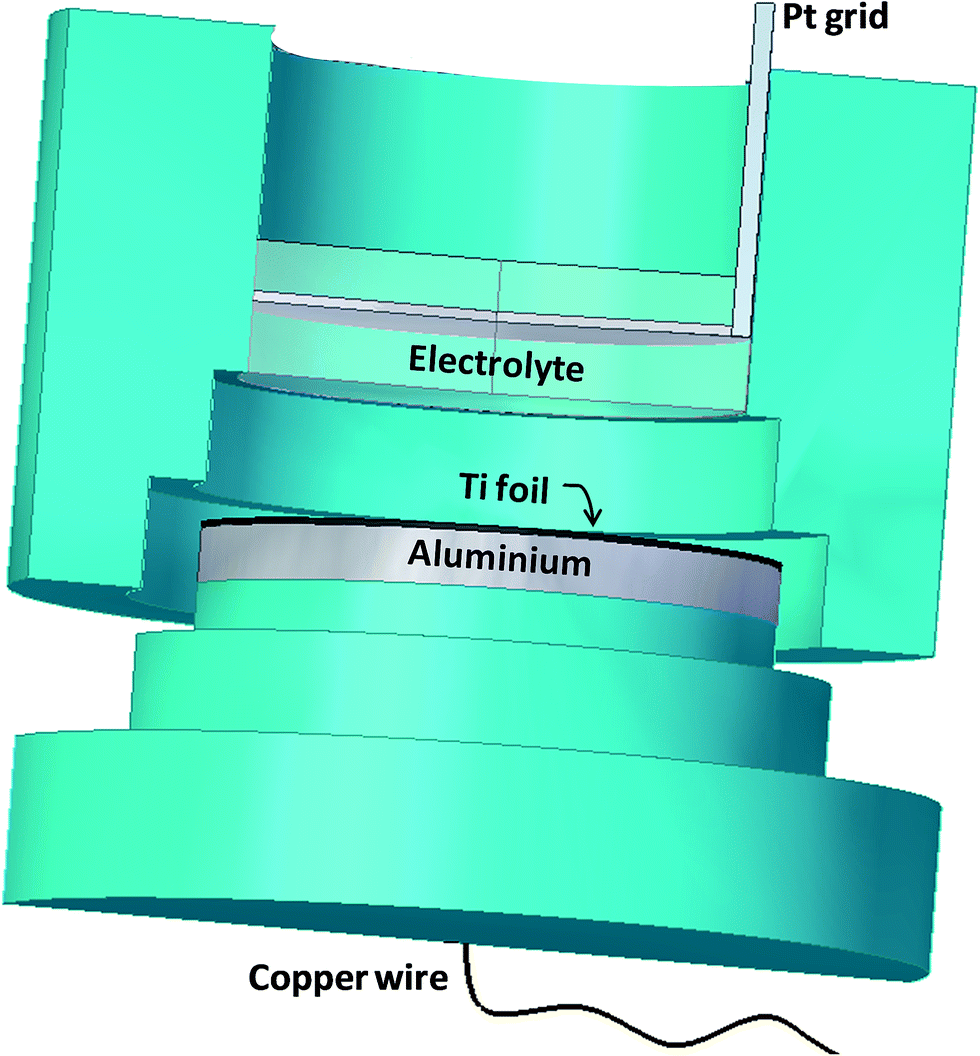 | ||
| Fig. 1 Electrochemical cell for the synthesis of TiO2 NT structures. | ||
The oxidation process was performed in (10%) deionized water/(90%) glycerol organic solution with 0.14 M of NH4F at room temperature. A potential ramp was imposed from the open circuit potential (OCP) to a fixed potential of 20 V with a scan rate of 100 mV s−1. Then, depending on the samples, this potential value was kept constant for either 0.5 or 4 hours in order to obtain different dimensions of the NTs. In the rest of the text the two kinds of samples will be referred to as NT-05 and NT-4, respectively.
A final annealing treatment was required in order to transform the amorphous structure into a crystalline one. Thermal treatment was performed in air atmosphere at 400 °C for 1 h.
The resulting structures were used either as final electrodes or as basic supports for the deposition of tungsten oxide, to obtain titania–tungsten oxide modified electrodes.
2.2 Electrodeposition of WO3
The electrodeposition of tungsten oxide was performed at room temperature in a classical three-electrode cell in which a platinum grid was the counter electrode. While the previously prepared supports were used as working electrodes, a saturated calomel electrode (SCE) was the reference: all the potential values in this experimental work are referred to it. The electrodes were connected to a potentiostat–galvanostat (Amel 7050) controlled by Junior Assist software. The electrolytic solution was prepared by dissolving sodium tungstate di-hydrate powder (Na2WO4·2H2O, 25 mM) in deionized water and by adding hydrogen peroxide (H2O2, 30 mM). The pH of the solution was adjusted to 1.5 by adding concentrated HNO3.A preliminary voltammetric study was performed which allowed individuating the main reductive wave at −0.3 V (data not shown). This potential value was adopted in the deposition process of tungsten oxide by potentiostatic runs. A PPT was used in order to obtain the oxide over-layer on the different substrates. During PPT, the potential was alternated swiftly between open circuit potential (OCP) and −0.3 V. A series of pulses of equal amplitude but different widths was performed. Each pulse consisted of an ON-time of 1 s during which −0.3 V was applied and an OFF-time of 10 s during which the electrode was maintained at the OCP value.
Specific samples were also prepared in order to investigate the effect of the tungsten oxide amount on the photoactivity of the samples. For practical reasons, rather than progressively loading the same support, different samples (2 cm2) derived from the same disk (15 cm2) were used at which different loading times were applied. This procedure prevented the effects of the characterization tests of each deposit from somehow affecting the stability of the deposit itself, and its subsequent response to additional loading. NT-4 structure was selected for this kind of experiment: WO3 deposition times from a few seconds up to 300 s were adopted. The number of pulses required to reach the proposed deposition times was calculated according to the ON-time duration. At the end of each experiment, the total amount of charge passed during the ON-time intervals in the PPT runs was recorded. Values between 0.07 and 1.85 C cm−2 were evaluated with respect to the nominal geometric area.
The obtained TiO2–WO3 modified samples were annealed in air atmosphere at 450 °C for 2 h.
Final samples on which deposits of tungsten oxide were obtained are indicated in the rest of the text as X/Wy, where “X” indicates the type of substrate and “y” the deposition time of the tungsten oxide, in seconds.
2.3 Characterization of the samples
Morphological characterization of the samples and elemental mapping analysis were performed by means of scanning electron microscopy (SEM) equipped with EDX detector, (Zeiss Supra 40 FEG-SEM). Focused ion beam (FIB) was also used to obtain precise cross sections of the nanotubular samples for subsequent imaging via SEM.Raman measurements were performed in order to reveal the crystalline phase of the different layers. These measurements were performed in air at room temperature using a BWTEK i-Raman Ex integrated system compact spectrometer, with an excitation wavelength at 1064 nm (provided by a Nd:YAG laser), in backscattering geometry. The spectra were collected with a very low power beam (<5 mW) focalized in 1 mm2 through a microscope objective Olympus ×20 to avoid any heating effect.
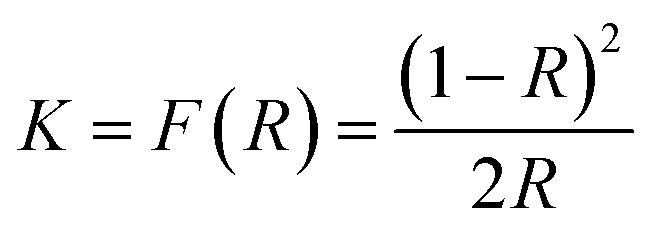
Diffuse reflectance UV-vis spectra of the bare and WO3 modified samples were recorded by a spectrophotometer (Agilent Cary 100). The reflectance spectra were analyzed by using the Kubelka–Munk relation which transforms the measured reflectance, R, into a Kubelka–Munk function K which may be associated with the absorption coefficient:18
 | (1) |
The variation of the Kubelka–Munk function with photon energy, (Khν)1/2 vs. hν, was used to estimate the energy-gap of the samples.
Photoelectrochemical characterization of all the samples was performed in an undivided three-electrode cell equipped with a quartz window. The synthesized materials were used as working electrodes, while platinum constituted the counter electrode. Also in this case, SCE was used as a reference. 0.1 M KNO3 aqueous solution was used as the supporting electrolyte. Depending on the experiments, a fixed amount of glycerol (10%) was added to the electrolyte, as a hole scavenger, to investigate on the extent of the photogenerated charges recombination (CR) in the examined structures. The same electrochemical cell was also used to study the voltammetric behavior of the deposits in 0.1 M HNO3 aqueous solution under dark conditions.
The photoactivity of the samples was tested under a light flux provided by a 300 W Xe lamp (Lot Oriel) equipped with an IR water-filter. Suitable optical filters were used in order to select different wavelengths of the incident light. Chronoamperometric tests were performed at 0.5 V of overpotential from the OCP of each sample: it was verified that such bias potential was enough to saturate the photocurrent. For all the cases, the photocurrent was calculated by subtracting the stable value measured in the dark from that obtained under irradiation. Photocurrent density values were calculated with respect to the nominal area. The incident power density (W cm−2) of the light was measured by LP 471 UVU or LP 471 PAR quantum radiometric probes: its value was used as normalizing factor, when the comparison of the results obtained at the different wavelengths was needed (normalized photocurrent, NPC).
Photo-electrochemical impedance spectroscopy (P-EIS) measurements were performed at the open circuit potential, in 0.1 M KNO3, under different irradiation conditions. The investigated frequency range was from 105 Hz to 10−2 Hz. In some cases, P-EIS runs were also performed in 0.1 M KNO3/10% (v/v) glycerol solution.
Specific investigation was performed in order to verify the homogeneity of the NT structure obtained on the sample of 15 cm2 of nominal area, prepared as described in Section 2.1. Different runs were performed in which a Teflon holed mask allowed one section at time to be exposed to the solution and to the irradiation. Fig. 2 reports, as an example, the values of photocurrent density obtained at the different points of the active surface when the NT-4 sample was irradiated with white light.
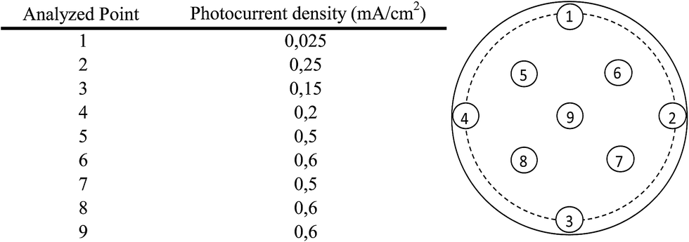 | ||
| Fig. 2 Photocurrents density (mA cm−2) distribution at TiO2 nanotubular sample irradiated with white light. Data refers to NT-4 sample. | ||
The data indicates a regular performance of the NTs if we exclude the border effects (5–6 mm, about corresponding to the thickness of the wall of the cylindrical cell). The uniformity of the structure was also confirmed by the relevant SEM analyses performed at the same indicated points (data not shown). The peripheral part of the disk was cut, so that only the uniform central part of the sample was used in order to derive the supports where deposit of WO3 was obtained. Samples of 2 cm2 of nominal area were generally used.
3. Results and discussion
As the synthesis of mixed oxide samples is considered, different mechanisms could be involved during the electrochemical deposition of tungsten oxide.19–21 Fig. 3 depicts the trend of the charge passed during WO3 deposition at the CTO and NT samples, adopted as supports in the present work. A regular increasing trend of the electrical charge is measured for the NT structures, which could correspond to an increasing in the amount and/or thickness of the oxide layer. However, the plateau measured at CTO could not be interpreted as a passivation state of the sample because, although charge is not increased, the deposition might have occurred by precipitation, due to possible pH gradients originated in the vicinity of the electrode surface.19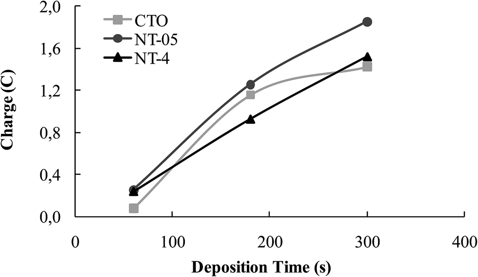 | ||
| Fig. 3 Charge (C) passed during different WO3 electrodeposition times at the CTO, NT-05 and NT-4 supports. | ||
The increasing amount of the deposit, obtained at NT-4 support is assessed by the results in Fig. 4, where the trend of the linear sweep voltammetry (LSV), obtained in acidic solution is reported. At all the tungsten oxide modified samples, two reduction peaks appear at −0.2 V and −0.45 V, the height of which increases in samples where WO3 deposition time was higher. The two peaks may be attributed to the phase transition, W6+/W5+ (peak I) and W5+/W4+ (peak II), while the sharp increase of the cathodic current at −0.55 V may be related to hydrogen evolution.22
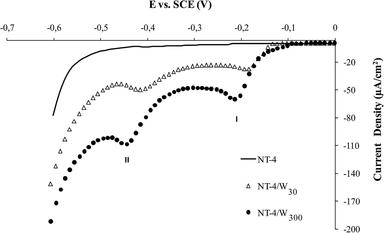 | ||
| Fig. 4 LSV recorded at NT-4/Wy (y = 30 and 300 s) in 0.1 M HNO3 aqueous electrolyte. The scan at NT-4 bare support is also reported as a comparison (continuous black line). Potential scan rate: 1 mV s−1. Data recorded under dark conditions. | ||
Fig. 5 gives an example of the Raman spectra of NT-4 support, as a bare structure, or with 300 s of tungsten oxide loading. Data confirms that anatase is the prevailing phase of the supports, while different phases are present in the tungsten oxide over-layer. In fact, the spectrum registered on the TiO2 electrodes reveals the well-known Raman features of the anatase phase: 144 (Eg)*, 197 (Eg), 399 (B1g)*, 513–519 cm−1 (A1g mode superimposed with B1g mode)*, and 639 (Eg)* cm−1, with the strongest vibrations identified by asterisk.23 As the support modified by tungsten oxide is considered, new peaks appear at about 270 and 320 cm−1, and in the 715 and 810 cm−1 range, due to the overlapping of the contributions from the different phases of tungsten oxide (bending and stretching vibration of the O–W–O modes).
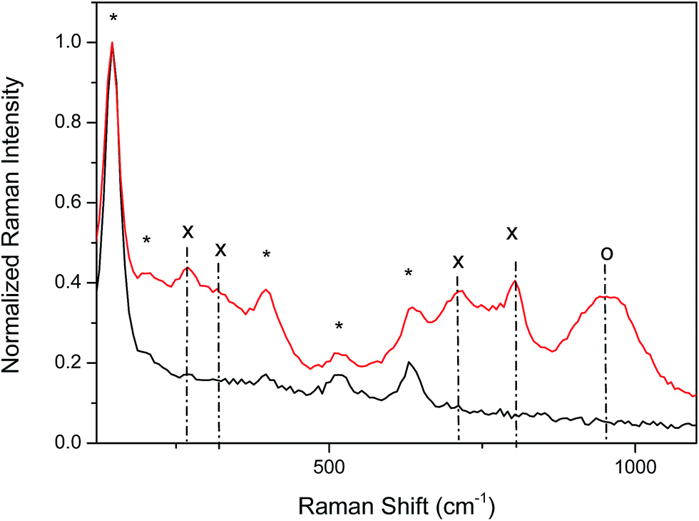 | ||
| Fig. 5 Raman spectra of TiO2 (black line) and NT-4/W300 (red line). (*) identifies the peaks from TiO2 anatase phase; (x) indicates the peaks related to WO3 phases, while (o) indicates the Raman feature related to WO5 and WO6 phases. | ||
In particular, the features related to the WO3 γ-phase (monoclinic, space group P21/n) and the β-phase (orthorhombic space group Pnma) are the most probable.24 The presence of both phases is somewhat an expected result with the transition temperature (350 °C) being very close to the annealing temperature utilized (450 °C).25,26 The broad peak at about 950 cm−1 is not related to any phase of the WO crystal, but to the overlapping of defect modes related to the presence of other oxides in which tungsten has a higher coordination level (such as WO5 or even WO6).27,28 For this reason, in the rest of the text, the over-layer of tungsten oxide will be indicated as WOx.
Fig. 6 reports the trend of the Kubelka–Munk function with photon energy, (Khν)1/2 vs. hν, recorded at the NT-4/W300, NT-4/W60 and NT-4 samples.
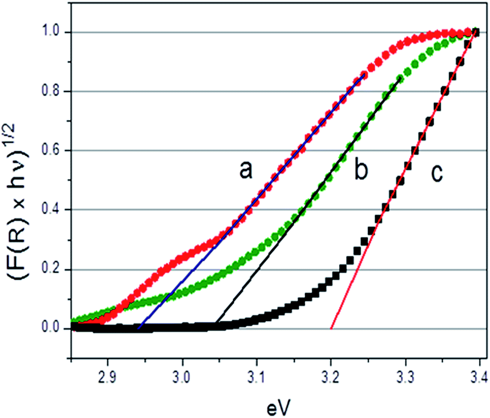 | ||
| Fig. 6 Normalized absorbance curves (F(R) × hν)1/2 vs. hν (eV) for the NT-4/W300 (a), NT-4/W60 (b) and (c) NT-4 electrodes. | ||
As it can be observed, increasing deposition times of the tungsten oxide, causes an apparent narrowing in the measured band gap. This behavior can be attributed to the different thickness of the tungsten oxide layer: a decrease of the band gap from about 3.05 to 2.6 eV was reported, when the thickness of the WO3 layer passed from 200 to 1400 nm.29
Moreover, a second active zone (see curve a in Fig. 6) in the spectrum region of low energies (hν < 3.05 eV) is observed at highly loaded sample, that could be due to intra-gap states, related to the different oxide species (evidenced by the Raman spectra), which can be differently involved depending on the wavelength considered. However, an increase of the incident light absorption capacity is not directly related to an increase of the system photoactivity. In fact, to improve the photocatalytic response of the material, low recombination rates between the photogenerated charges and good charge transport capability are also required.15
In order to investigate on the possible effects of the substrates, Fig. 7 shows an example of the morphology of the compact and nanotubular structures used as support for the subsequent WOx deposition.
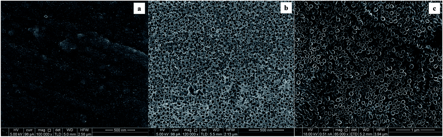 | ||
| Fig. 7 SEM micrographs of TiO2 bare supports: CTO (a), NT-05 (b) and (c) NT-4. | ||
A granulated structure is revealed at CTO, while nanotubes of different dimensions (mean diameter ranging from 20 to 80 nm) were obtained depending on the oxidation time. Moreover, an enhancement in the uniformity of the pore distribution, as well as in the definition of the NT structures was observed at longer anodization times (Fig. 7c). According to the literature,17,30,31 experimental conditions such as kind of electrolyte and anodization time may actually influence both the diameter and the length of tubes: in the present case the average length of the nanotubes increased from about 200 to 600 nm with increasing anodization time from 0.5 to 4 hours (Fig. 8).
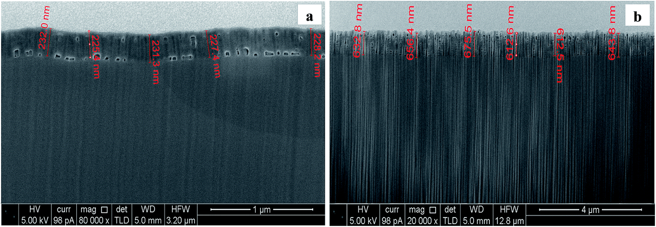 | ||
| Fig. 8 SEM micrographs of FIB cross sections of the TiO2 nanotubes obtained at the NT-05 (a) and (b) NT-4 supports. | ||
The nature of the substrate can influence the eventual size and shape, as well as the final electrodeposition efficiency.7 SEM micrographs of the relative WOx deposits obtained at the different supports are reported in Fig. 9: a high loading of tungsten oxide is considered (y = 300 s) to have a better picture of the morphology. A predominant compact tungsten oxide layer is representative of the CTO/W300 sample (Fig. 9a). A full coverage of the initial nanotubular structures is observed for both NT samples (Fig. 9b and c), at which different crystal shapes are observed: the deposit at the NT-05/W300 sample growths as 2D nanoplates like crystals, which remains fairly distinguishable during deposition time, while an aggregation of spherical nanoparticles is observed at the NT-4/W300. The elemental map of this last sample along with the corresponding SEM micrograph is reported in Fig. 10.
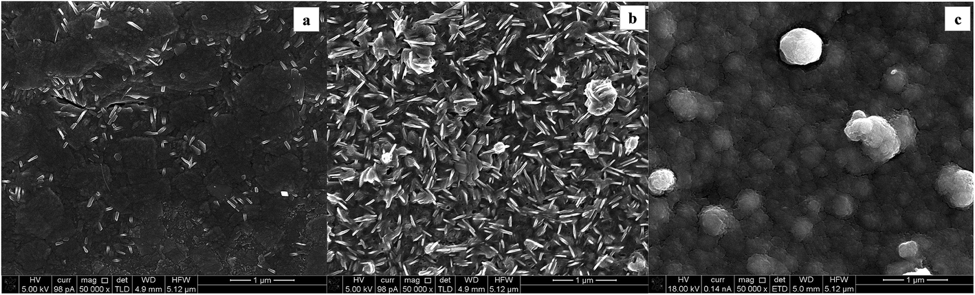 | ||
| Fig. 9 SEM micrographs of WOx modified supports: CTO/W300 (a), NT-05/W300 (b) and (c) NT-4/W300. | ||
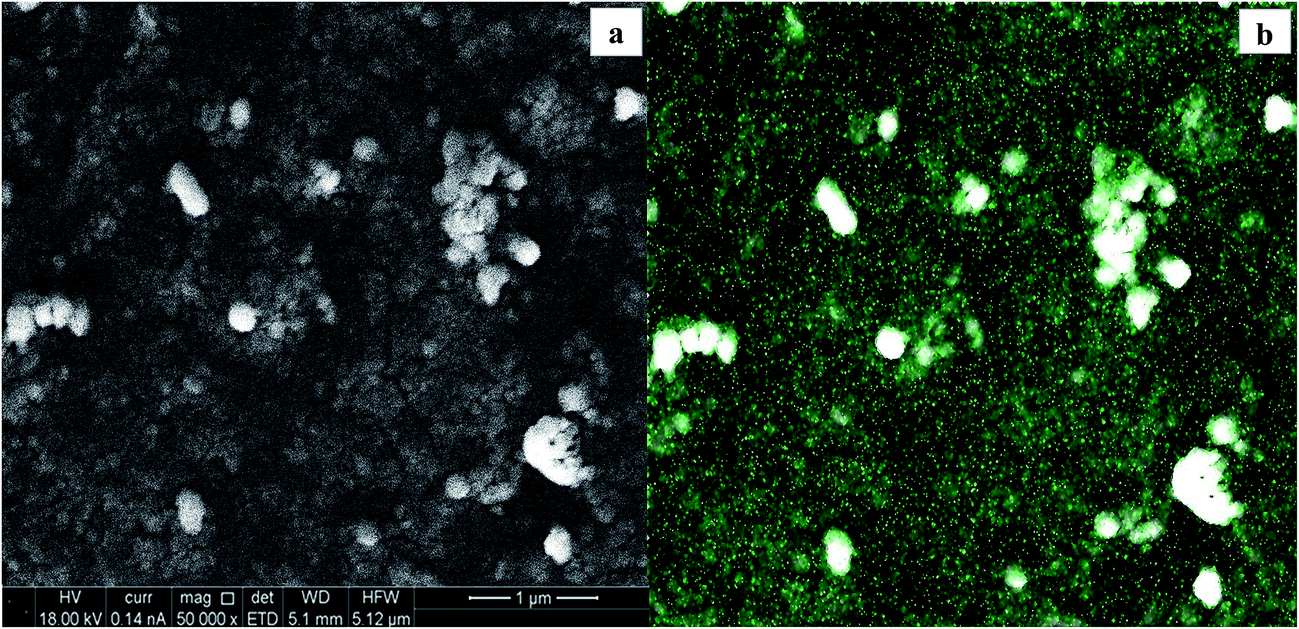 | ||
| Fig. 10 SEM micrograph of the NT-4/W300 scanned area (a) and (b) elemental map of the tungsten (green dots) at the WOx deposit. | ||
As the photoactivity is concerned, Fig. 11 shows an example of the polarization curves obtained at a WOx modified sample: in all the cases, negligible current values are observed under dark conditions, while the working of the structure is assessed under illumination. The NPC reaches a saturation value at about 0.3 V, while oxygen evolution starts to occur at a potential higher than 1.4 V. The inset of the same figure reports an example of a chronoamperometric test performed at 0.5 V of overpotential from the OCP, from which the values of NPC were derived for the comparison of the performances of the different samples.
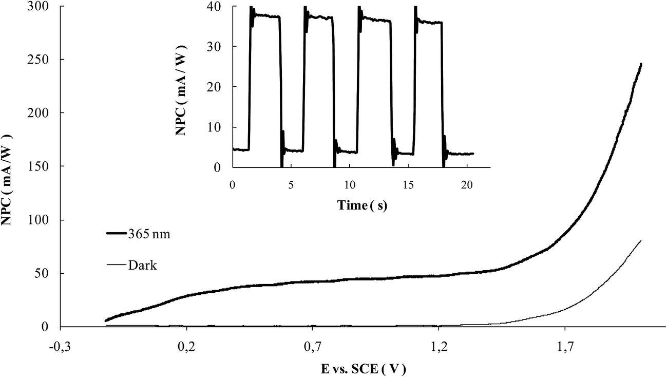 | ||
| Fig. 11 Example of the polarization curves recorded at NT-4/W10 in a 0.1 M KNO3 aqueous electrolyte. The potential was ramped (10 mV s−1) from the OCP to 2 V; inset: example of the chronoamperometry test performed at the NT-4/W10 sample. Data recorded under irradiation (365 nm) and dark conditions. | ||
Data resumed in Table 1 also demonstrate that samples are photoactive, regardless the kind of support where WOx is deposited.
| Sample | CTO | CTO/W300 | NT-05 | NT-05/W300 | NT-4 | NT-4/W300 |
|---|---|---|---|---|---|---|
| NPC365 (mA W−1) | 3.02 | 0.99 | 7.57 | 1.60 | 11.83 | 6.80 |
| NPC400 (mA W−1) | 0.36 | 0.27 | 0.63 | 0.27 | 0.93 | 2.11 |
The observed behavior seems to be in contrast with that expected for the Ti/TiO2/WOx combined structure. With this disposition, if the photogenerated charge transfer mechanism were only determined by the reciprocal position of the energy levels of the band edges of the semiconductors, the activity of the combined structure could be negatively affected. Transfer of electrons accumulated in the CB of WOx, towards the counter electrode, and the capture of holes in the VB of the TiO2 by electron donors in solution could be difficult, in particular at high WOx cover levels, when the inner surface of the nanotubes is not easily reachable by the electrolyte, or the TiO2/electrolyte interface is limited.
Two factors may determine the observed behavior of our samples. Actually, as reported in the introduction, when a suitable light irradiates the WOx particles that cover the TiO2 sites, an increase of the quasi-Fermi level of WOx may be originated by the injection of electrons in its CB, and this could reverse the charge transfer mechanism (Fig. 12a). But also, it is worth to consider that the porous structure of nanotubular support may play an important role. Due to the high concentration of defects which may be present at the surface of NTs,3 the interlayer between the two semiconductors may result quite conductive, so that also a Z-mechanism could activate the charge transfer. In this way electrons left in the CB are free to be sent to the Ti surface (to which the anodic potential is applied), and in turn to the counter electrode. In the meanwhile, free holes in the VB of WOx may oxidize water (Fig. 12b). Depending on the wavelength, one or both the mechanisms could be active in determining the charge transfer flow at mixed oxide sites. Obviously, at TiO2 not covered by WOx, the charge transfer can occur, by the mechanism expected at n-type semiconductors, by which holes are available at the VB, to react with the electrolyte, provided it is able to contact the electrode interface.
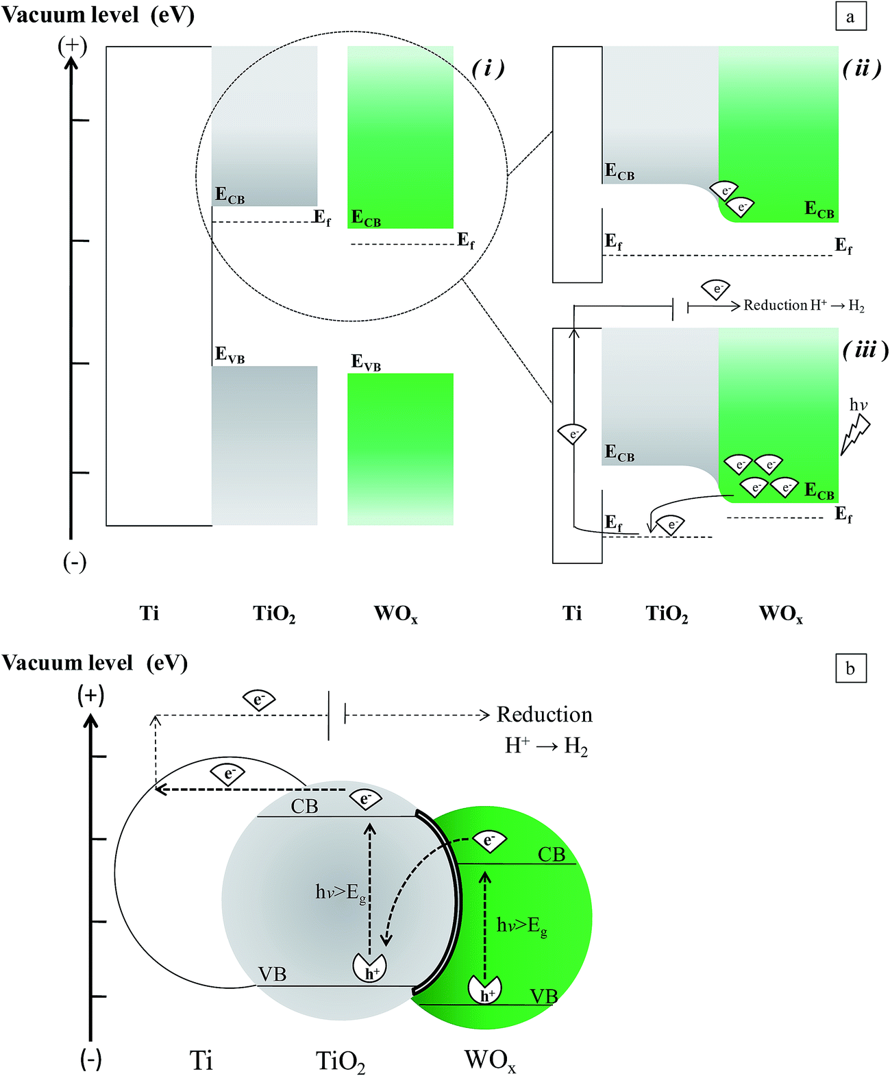 | ||
| Fig. 12 Scheme of the two proposed mechanisms of charge transfer at Ti/TiO2/WOx. (a) Shift of quasi-Fermi level: before (i) and after (ii) the contact of the phases, under dark conditions; (iii) under irradiation. (b) Z-Scheme. | ||
Some further consideration may be done, on the basis of data in Table 1. If the data of bare TiO2 are considered, since the heterogeneous character of the involved reactions, when passing from compact to tubular structure, a significant enhance of the performance is obtained, mainly due to the high specific area of the porous NT support; also a faster charge transport can be achieved, so that an enhancement in the photocurrent is observed. Moreover, data evidence the benefit of using the well-defined nanotubular structures, also as the supports in the combined oxide samples: at both wavelength values, the longer the oxidation time in the synthesis of NTs, the higher the measured photocurrent in the resulting sample. However, when compared with the relevant bare supports, the behavior of the mixed oxide samples was not so encouraging. Actually, adding the second oxide resulted to be convenient only at NT-4 support and at 400 nm of light wavelength.
However, it must be observed that high coverage level was achieved in all samples in Table 1, so investigation on the effect of the amount of WOx, kind of support being the same, was further undertaken. To this aim, the best performing structure, with the most regular deposition curve (NT-4, see Fig. 3), was selected as support: deposition times were ranged from 2 s to 300 s. Fig. 13 resumes the results obtained at the two wavelengths.
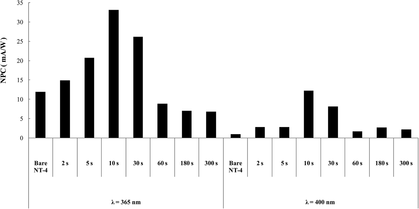 | ||
| Fig. 13 NPC (mA W−1) for the bare and WOx modified NT-4 samples. Data obtained at 365 and 400 nm in 0.1 M KNO3. | ||
Similar trends of photocurrents were observed at the two wavelengths, confirming that in both the cases, an optimum in the deposit was reached, at which the use of mixed oxides was convenient: the sample treated for 10 s resulted the best performing at both the wavelengths. SEM analysis (Fig. 14) indicated that at this sample the nanotubular structure is still evident, deposition of WOx occurring mostly at the walls of tubes.
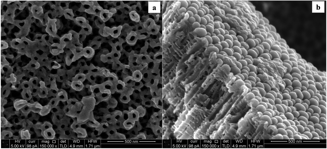 | ||
| Fig. 14 SEM micrographs of the NT-4/W10 (a) and (b) NT-4/W300 electrodes. | ||
The negative effect observed at higher loading could be due either to an increase in the CR, or to a decrease in the specific area of the electrode: plugging of NTs by WOx particles could reduce the TiO2/electrolyte interface.
3.1 Use of glycerol as hole scavenger
On the basis of the photocurrent data reported above, an investigation was performed on the photoactivity in the presence of a hole scavenger, such as glycerol, allowing for the derivation of indications on the mechanism of the CR at these samples.Fig. 15 compares the performances, in terms of photocurrent, obtained in the presence of glycerol when the NT-4/Wy electrodes were irradiated at 365 nm and 400 nm. Data related to the bare NT-4 support is also reported in the graphs as a comparison. To make the comparison straightforward, the parameter γ has been introduced, defined as the ratio between the values measured in the presence of the scavenger and in the supporting electrolyte. This parameter can be considered as a measurement of the CR in the original sample: a high value of γ indicates the beneficial effect obtained by adding glycerol, which was able to scavenge the holes.
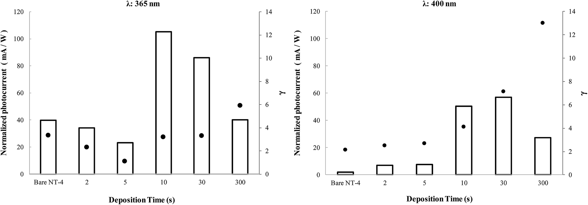 | ||
| Fig. 15 NPC (white bars) at NT-4 and NT-4/Wy samples, measured at 365 and 400 nm in 0.1 M KNO3/10% glycerol electrolyte. γ values (black points) are defined as ratio between the photocurrents measured in the presence of the scavenger and in the supporting electrolyte. | ||
In all the experimental conditions, in the presence of glycerol, a significant enhancement of the performance of all the samples was observed (γ > 1), indicating a strong effect of the scavenger at both investigated wavelengths. The γ value at NT-4/W300 could give an indication of the extent of the recombination at WOx: as indicated by the SEM analyses, at this deposition time, all of the NT-4 nanotubular structure is covered by the WOx layer, so that it is the only phase contacting the electrolyte. A comparison between γ values at NT-4 and NT-4/W300 indicates that at both the wavelengths, CR at WOx is higher than at TiO2. Although WOx is able to absorb the radiation, a high concentration of defects, which act as CR sites, could be the reason of this result.32
However, if the trend of γ is considered as the WOx loading is increased (Fig. 15), a different importance of the CR may be derived at the two wavelengths. At 400 nm, the TiO2 substrate has a negligible photoactivity with respect to that of WOx: an initial nearly constant trend of γ is calculated, then its value is nearly doubled after the first 10 s of deposition, and it further increases for samples with higher loading. In this case, although the addition of small amounts of WOx involves a benefit in terms of photocurrent, it does not seem to affect the performance of the sample in terms of CR. In fact, the nearly constant γ values, observed at low WOx coverage, indicate that the increase of the recombination sites due to the WOx deposit, is negligible compared to original CR at the surface of TiO2.
At 365 nm, when both the phases are activated by the incident light, a minimum is observed. Two contrasting effects can be considered to justify this trend: on the one hand, at low coverage levels, the presence of WOx reduces the CR due to the possible interactions between electronic bands, as described above, which allows a higher separation of the photogenerated charges. By contrast, as the coverage level increases, the TiO2 surface is being partially covered by a less active material (WOx): CR at WOx becomes the prevailing negative effect. Thus, after a certain coverage degree, when all the TiO2 nanotubular structure is practically covered, WOx is the only phase in contact with the electrolyte. In such a situation, the decrease in the photocurrent in KNO3 (Fig. 13) at both wavelengths may be mainly due to a decrease in the electrode active surface. The increase in the γ values indicates that, for these loadings, high WOx deposit amounts also results in a significant increase of recombination sites: actually, for these samples the positive effect of glycerol is the highest.
3.2 EIS analysis of the best performing sample
Further information about the charge transfer at the best performing sample was obtained from the P-EIS measurements in the presence and absence of glycerol. The relevant impedance spectra of the NT-4 and NT-4/W10, under illumination (λ = 365 nm and 400 nm), measured at the open circuit potential are shown in Fig. 16 in terms of Nyquist plots. Two semi-circles are generally identified, respectively at the high and medium frequency region. Depending on the case, a third element appeared in the impedance spectra.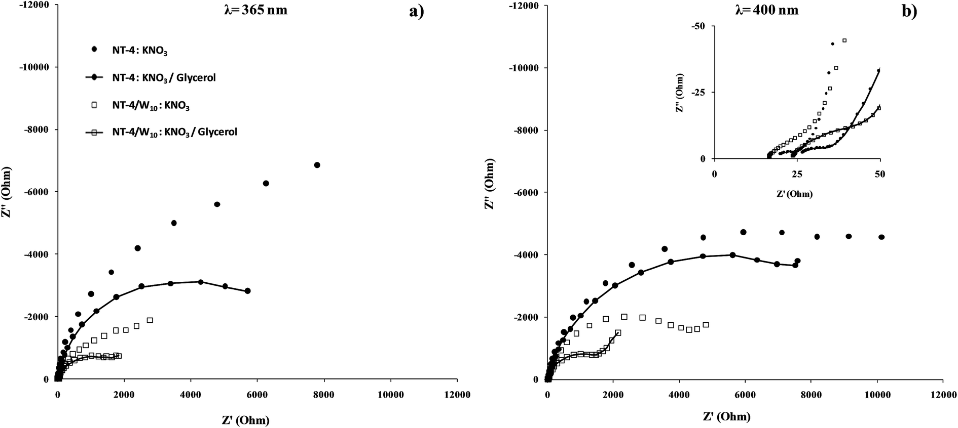 | ||
| Fig. 16 Nyquist plots of the NT-4 and NT-4/W10 samples obtained at the open circuit potentials at 365 (a) and (b) 400 nm in 0.1 M KNO3 or 0.1 M KNO3/10% glycerol electrolytes. | ||
As a qualitative comparison is concerned, at both the wavelengths, the P-EIS spectra recorded at the combined system (NT-4/W10) are lower than that related to the single phase (NT-4), which suggests that the presence of WOx at the NT structure enhances the TiO2 phase performance. Moreover, for both the investigated samples, the positive effect of glycerol is evidenced: lower P-EIS data are obtained in the presence of the scavenger, with respect to those obtained in the absence of the organic solute.
The quantitative analysis of the data was performed using the equivalent circuit approach. Two electrical circuits were selected to fit the P-EIS data derived from the measurements performed at the NT-4 and NT-4/W10 samples, and to obtain the circuital parameters. Fig. 17a shows the equivalent circuit employed to describe the NT-4 behavior: two RQ elements in series with a Rs, correlated with the solution resistance (mean value around 20 Ω), were employed to describe the performance of the NT-4 sample. Constant phase elements, CPE (1/Z = Q(jω)n), rather than perfect capacitances were used, where the displacement from unity of the exponent “n”, accounts for the non-ideality of the capacitor. In the presence of the second oxide (WOx), an additional impedance, a Warburg element, was needed to fit the data at the lowest frequencies for the NT-4/W10 system (see Fig. 17b).
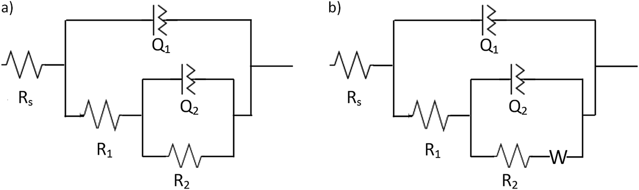 | ||
| Fig. 17 Equivalent circuits used to fit the EIS data obtained at the open circuit potentials under irradiation conditions (365 and 400 nm) in 0.1 M KNO3 or 0.1 M KNO3/10% glycerol electrolytes for the NT-4 (a) and (b) NT-4/W10 samples. | ||
The circuital parameters are summarized in Table 2.
| Sample | NT-4 | ||||||||
|---|---|---|---|---|---|---|---|---|---|
Electrolyte solution ![[thin space (1/6-em)]](https://www.rsc.org/images/entities/char_2009.gif) |
Wavelength, nm | R1, Ω cm2 | Q1, × 105, S sn cm−2 | n1 | τ1 × 10³, s | R2, Ω cm2 | Q2 × 105, S sn cm−2 | n2 | τ2, s |
| 0.1 M KNO3 | 365 | 19.1 | 9.1 | 0.72 | 0.14 | 28313 |
29.1 | 0.98 | 8.64 |
| 400 | 22.8 | 6.2 | 0.69 | 0.07 | 24000 |
9.9 | 0.96 | 2.46 | |
| 0.1 M KNO3/10% glycerol | 365 | 31.3 | 9.7 | 0.78 | 0.56 | 13804 |
32.4 | 0.97 | 4.72 |
| 400 | 33.9 | 5.3 | 0.67 | 0.08 | 18750 |
10.3 | 0.90 | 2.08 | |
| Sample | NT-4/W10 | |||||||||
|---|---|---|---|---|---|---|---|---|---|---|
| Electrolyte solution | Wavelength, nm | R1, Ω cm2 | Q1 × 105, S sn cm−2 | n1 | τ1 × 10³, s | R2, Ω cm2 | Q2 × 105, S sn cm−2 | n2 | τ2, s | W, S s1/2 |
| 0.1 M KNO3 | 365 | 35.7 | 22.5 | 0.71 | 1.18 | 4393 | 85.3 | 1 | 3.75 | 0.00470 |
| 400 | 40.9 | 5.8 | 0.80 | 0.52 | 6696 | 19.2 | 1 | 1.28 | 0.00269 | |
| 0.1 M KNO3/10% glycerol | 365 | 48.4 | 20.3 | 0.69 | 1.20 | 2093 | 61.8 | 1 | 1.29 | 0.00447 |
| 400 | 67.6 | 10.3 | 0.70 | 0.85 | 2128 | 40.5 | 1 | 0.86 | 0.00282 | |
The time constant values, calculated as τ1 = (R1 × Q1)1/n1 and τ2 = (R2 × Q2)1/n2, also reported in the same table, allowed to individuate the different steps involved in the processes.
According to the data shown in Table 2, R1Q1 can be related to the CR process occurring at the bulk of the semiconductor material: under the experimental conditions adopted in this work, the related time constant (τ1) values in the order of milliseconds were actually obtained, which are consistent with the lifetime of the photogenerated charges.33
The time constants (τ2) related to the R2Q2 element indicate a slower process, which may be referred to a charge transfer process, at the electrode/electrolyte interface. Therefore, the R2 can be described by a charge transfer resistance (RCT).34
In the case of the NT-4/W10 sample, the Q2 is a perfect capacitor (n = 1), and the related τ2 decreases if compared to the corresponding value for NT-4 sample. However, the presence of a third element (Warburg impedance) in the equivalent circuit may evidence the existence of diffusion effects, perhaps caused by the presence of WOx nanoparticles inside the nanoporous structure, which may limit the diffusion of the electrolyte within the nanotubes.
The obtained results confirmed that both the recombination resistance (R1) and the lifetime of the charges (τ1) increase at both the wavelengths when WOx is present in the sample, and a further increase is observed, especially at 400 nm when glycerol was used as hole scavenger. Lower RCT values are obtained when the combined structure was used: a better separation of the photogenerated carriers may lead to a greater availability of holes for the oxidation of either water or organic compound, which can be confirmed by the subsequent decrease of RCT values in the presence of the scavenger. τ2 data also confirms a faster charge transfer process occurring at the NT-4/W10 surface/electrolyte interface (rather than the one observed at the NT-4 sample), and especially the improvement due to the presence of glycerol which acts as scavenger.
4. Conclusions
The presented results gave evidence on the effectiveness of combining tungsten oxide with well-developed TiO2 nanotubes. However, a real benefit is obtained only if a partial coverage by the WOx is maintained, whereas at the highest coverage degree, the prevailing effects are the increasing of charge recombination at WOx, and the decreasing extent of the interface electrode/electrolyte, due the plugging of NTs.The NT-4/W10 was individuated as the best performing sample, which at both the wavelengths represented a good compromise to obtain high photocurrents in KNO3, keeping CR as low as possible.
Taking into account for both the light and the anodic potential to which the samples are submitted, the benefit obtained at the mixed oxide samples, has been explained as due to two main mechanisms.
On one hand, the Z-scheme may be activated thanks to the conductive nature of the nanotubular surface. It may constitute a suitable interlayer which activates a charge transfer mechanism, allowing electrons at TiO2 CB and holes at WOx VB, to be transported to the counter electrode, or available for the electrolyte, respectively. Such a mechanism may be the most favored under the irradiation of λ = 365 nm, when both the semiconductors are photoactivated. On the contrary, at λ = 400 nm, when the photoactivity of WOx is predominant compared to that of TiO2, the main charge transfer mechanism could be activated by the shift of the quasi-Fermi level. Due to the irradiation, a non-equilibrium state could be originated by the “hot” electrons injected into the WOx CB, so that the quasi-Fermi level of WOx could become higher than that of TiO2 (Fermi level of TiO2 remained about constant, due to its scarce photoactivity at 400 nm).
Acknowledgements
The authors wish to thank Sotacarbo SpA for the financial support, Ettore Dedola for participating to the experimental measurements, and David Measley and James Kilgannon for their help in editing the document.References
- K. Chen, Z. Jiang, J. Qin, Y. Jiang, R. Li, H. Tang and X. Yang, Ceram. Int., 2014, 40, 16817 CrossRef CAS.
- H. Tang, D. Zhang, G. Tang, X. Ji, W. Li, C. Li and X. Yang, Ceram. Int., 2013, 39, 8633 CrossRef CAS.
- S. Palmas, A. Da Pozzo, M. Mascia, A. Vacca, R. Matarrese and I. Nova, J. Appl. Electrochem., 2012, 42, 745 CrossRef CAS.
- X. Yang, J. Qin, Y. Jiang, K. Chen, X. Yan, D. Zhang, R. Li and H. Tang, Appl. Catal., B, 2015, 167, 231 CrossRef.
- X. Yang, J. Qin, Y. Jiang, R. Li, Y. Li and H. Tang, RSC Adv., 2014, 4, 18627 RSC.
- G. Hodes, D. Cahen and J. Manassen, Nature, 1976, 260, 312 CrossRef CAS.
- T. Zhu, M. N. Chong and E. S. Chan, ChemSusChem, 2014, 7, 2974 CrossRef CAS PubMed.
- V. S. Vidyarthi, M. Hofmann, A. Savan, K. Sliozberg, D. König, R. Beranek, W. Schuhmann and A. Ludwig, Int. J. Hydrogen Energy, 2011, 36, 4724 CrossRef CAS.
- S. S. Kalanur, Y. J. Hwang, S. Y. Chae and O. S. Joo, J. Mater. Chem. A, 2013, 1, 3479 CAS.
- S. Yousefzadeh, A. Reyhani, N. Naseri and A. Z. Moshfegh, J. Solid State Chem., 2013, 204, 341 CrossRef CAS.
- A. Watcharenwong, W. Chanmanee and N. R. De Tacconi, J. Electroanal. Chem., 2008, 612, 112 CrossRef CAS.
- A. K. L. Sajjad, S. Shamaila, B. Tian, F. Chen and J. Zhang, Appl. Catal., B, 2009, 91, 397 CrossRef CAS.
- Y. C. Nah, A. Ghicov, D. Kim and P. Schmuki, Electrochem. Commun., 2008, 10, 1777 CrossRef CAS.
- I. Paramasivam, Y. C. Nah, C. Das, N. K. Shrestha and P. Schmuki, Chem.–Eur. J., 2010, 16, 8993 CrossRef CAS PubMed.
- S. Bai, J. Jiang, Q. Zhang and Y. Xiong, Chem. Soc. Rev., 2015, 44, 2893 RSC.
- M. Miyauchi, A. Nakajima, T. Watanabe and K. Hashimoto, Chem. Mater., 2002, 14, 4714 CrossRef CAS.
- S. Palmas, A. Da Pozzo, F. Delogu, M. Mascia, A. Vacca and G. Guisbiers, J. Power Sources, 2012, 204, 265 CrossRef CAS.
- H. Lin, C. P. Huang, W. Li, C. Ni, S. I. Shah and Y. H. Tseng, Appl. Catal., B, 2006, 68, 1 CrossRef CAS.
- E. A. Meulenkamp, J. Electrochem. Soc., 1997, 144, 1664 CrossRef CAS.
- K. R. Reyes-Gil and D. B. Robinson, ACS Appl. Mater. Interfaces, 2013, 5, 12410 Search PubMed.
- N. R. De Tacconi, C. R. Chenthamarakshan, K. Rajeshwar, T. Pauport and D. Lincot, Electrochem. Commun., 2003, 5, 220 CrossRef CAS.
- S. Darmawi, S. Burkhardt, T. Leichtweiss, D. A. Weber, S. Wenzel and J. Janek, Phys. Chem. Chem. Phys., 2015, 17, 15903 RSC.
- G. Cappelletti, C. Ricci, S. Ardizzone, C. Parola and A. Anedda, J. Phys. Chem. B, 2005, 109, 4448 CrossRef CAS PubMed.
- S. Ardizzone, G. Cappelletti, C. Ricci and A. Sin, J. Nanosci. Nanotechnol., 2010, 10, 8367 CrossRef CAS PubMed.
- E. Salje and K. Viswanathan, Acta Crystallogr., Sect. A: Cryst. Phys., Diffr., Theor. Gen. Crystallogr., 1975, 31, 356 CrossRef.
- O. Berger, W. J. Fischer and V. Melev, J. Mater. Sci.: Mater. Electron., 2004, 15, 463 CrossRef CAS.
- K. J. Lethy, D. Beena, R. V. Kumar, V. P. M. Pillai, V. Ganesan and V. Sathe, Appl. Surf. Sci., 2008, 254, 2369 CrossRef CAS.
- K. K. Akurati, A. Vital, J. P. Dellemann, K. Michalow, T. Graule, D. Ferri and A. Baiker, Appl. Catal., B, 2008, 79, 53 CrossRef CAS.
- W. L. Kwong, N. Savvides and C. C. Sorrell, Electrochim. Acta, 2012, 75, 371 CrossRef CAS.
- W. Y. Wang and B. R. Chen, Int. J. Photoenergy, 2013, 2013, 1 Search PubMed.
- S. Palmas, M. Mascia, A. Vacca, J. Llanos and E. Mena, RSC Adv., 2014, 4, 23957 RSC.
- X. Li, F. Li, C. Yang and W. Ge, J. Photochem. Photobiol., A, 2001, 141, 209 CrossRef CAS.
- F. Le Formal, S. R. Pendlebury, M. Cornuz, S. D. Tilley, M. Grätzel and J. R. Durrant, J. Am. Chem. Soc., 2014, 136, 2564 CrossRef CAS PubMed.
- M. R. Hasan, S. B. A. Hamid, W. J. Basirun, S. H. M. Suhaimya and A. N. C. Mat, RSC Adv., 2015, 5, 77803 RSC.
| This journal is © The Royal Society of Chemistry 2016 |