High performance ternary solar cells based on P3HT:PCBM and ZnPc-hybrids

Burak Kadema, Aseel Hassan*a, Meltem Gökselbc, Tamara Basovade, Ahmet Şenocakb, Erhan Demirbaşb and Mahmut Durmuş*b
aMaterial and Engineering Research Institute, Sheffield Hallam University, UK
bGebze Technical University, Department of Chemistry, P.O. Box 141, Gebze, Kocaeli 41400, Turkey. E-mail: durmus@gtu.edu.tr
cKocaeli University, Kosekoy Vocational School, PO Box 141, Kartepe, Kocaeli, 41135, Turkey
dNikolaev Institutes of Inorganic Chemistry SB RAS, Lavrentiev Pr. 3, Novosibirsk 630090, Russia
eNovosibirsk State University, Pirogova Str. 2, Russia

Received 9th July 2016 , Accepted 22nd September 2016

First published on 22nd September 2016


Abstract

Single walled carbon nanotubes (SWCNTs) and reduced graphene oxide (rGO) covalently and non-covalently functionalised by zinc phthalocyanine (ZnPc) were added to P3HT:PCBM blend in order to investigate the effects of these hybrid materials on P3HT:PCBM organic solar cell performance. Adding a small amount of these hybrids to P3HT:PCBM blend does not significantly alter the absorption spectra of the latter nor its structure. ZnPc–rGO and ZnPc–SWCNT hybrid features have appeared on the P3HT:PCBM surface morphology as verified by SEM and AFM images. However these hybrid materials have caused significant effects on the electrical properties of the studied blends. An increase of about two orders of magnitudes has been observed in the electrical conductivity. Space charge limited conduction theory was employed to investigate the charge carriers' mobility whereas a thermionic emission model was used to evaluate the recombination rate based on an estimated diode ideality factor. Solar cell devices based on P3HT:PCBM:ZnPc–SWCNTs-co bonded have demonstrated best device performance with PCE of 5.3%, Jsc of 12.6 mA cm−2, Voc of 0.62 V and FF of 68%. A reference device based on bare P3HT:PCBM blend has exhibited PCE of just under 3.5%, Jsc of 9.3 mA cm−2, Voc of 0.62 V and FF of 60%.

Introduction

Nowadays, organic solar cells (OSCs) are considered as promising cost-effective, lightweight and appropriate candidates in role-to-role electronic technology. Despite their relatively low efficiency compared to the inorganic (such as silicon) solar cells, organic conjugated materials-based solar cells can be prepared via simple solution processing methods, which are compatible with flexible substrates.1 Recently, highly efficient OSC with a certified efficiency of 9.2% was reported for a device based on a single junction with an inverted structure configuration of ITO/PFN/PTB7:PC71BM/MoO3/Al.2 The latter has exhibited an ohmic contact for the photo generated charge-carriers and optimum light harvesting within the device. Conventionally, OSCs consist of conjugated polymer which acts as electron donor and a fullerene acting as an electron acceptor; these two materials usually blended together in certain ratios and sandwiched between two appropriately chosen electrodes with two different work functions. Among several organic materials studied in this respect, the poly(3-hexylthiophene) (P3HT) and [6,6]-phenyl C61-butyric acid methylester (PCBM) bulk heterojunction (BHJ) blend is considered as the most investigated donor/acceptor blend in OSCs.3–6 In order to achieve higher solar cell performance, it is crucial that a nanoscale interpenetrated network morphology of the blend is achieved. Such morphology is frequently shown to facilitate charge carriers separation and transportation, with exciton diffusion length in the range 10–20 nm.7,8 The band gap and the energy level alignment of the donor/acceptor within P3HT:PCBM blends could also lead to enhanced light absorption.9 Furthermore, it is worth stating that ternary blend is an encouraging concept to increase OSCs performance by either incorporation of complementary optical material or a material with higher charge carrier mobility or both. There are however two main restrictions in designing the ternary blends; these are the energy level alignment of the donor/acceptor in the blend and the distribution of the dopants within the blend.10 Functional materials such as single-walled carbon nanotubes (SWCNTs) with ballistic charge transport, high flexibility, and excellent mechanical and chemical stability are promising materials for ternary blend composites.11 On the other hand, reduced graphene oxide (rGO) or graphene are usually used as transparent electrodes12 or as novel alternatives to PEDOT:PSS hole transport layers13 as well as an acceptor within the organic solar cell blend.14 On the other hand, zinc phthalocyanine is an organic semiconductor material which has shown a promising application in organic solar cells with the potential of further enhancing the light harvesting properties of the blends due to its wide absorption bands in the near red region.15 The functionalization of SWCNTs by phthalocyanines has been shown to significantly enhance their optoelectronic16 as well as their sensing properties.17 (2-Aminoethoxy)(tri-tert-butyl)zinc phthalocyanine (AETBZnPc) has been covalently bonded to exfoliated graphene sheets in dichlorobenzene solvent to produce AETBZnPc–graphene hybrids which were used to fabricate a photo-electrochemical cell. The presence of electronic interactions in the excited states suggests a charge separation between the AETBZnPc and the graphene through the singlet excited state of AETBZnPc with prompt, steady, and reproducible photocurrent which makes this hybrid a potential candidate for solar cell applications.18 On the other hand the use of functional materials such as SWCNTs and rGO might have some disadvantages in this respect due to their possible contribution in compromising the device shunt resistance, as well as acting as charge recombination centres.19 Optimisation of carbon-based functional materials used in OSCs could however be achieved when small proportions of these materials are included in a controlled manner in these hybrids.10,20

In the current study, we have investigated the use of functional materials based on single walled carbon nanotubes (SWCNTs) and reduced graphene oxide (rGO) covalently (co) and non-covalently (non-co) functionalized with the 1-[N-(2-ethoxyethyl)-4-pentynamide]-8(11),15(18),22(25)-tris-{2-[2-(2-ethoxyethoxy)ethoxy]-1-[2-((2-ethoxyethoxy)-ethoxy)methyl]ethyloxy}zinc(II) phthalocyanine (ZnPc) and blended with P3HT:PCBM bulk heterojunctions (BHJs) as active layers for organic solar cell applications. The effects of ZnPc/rGO and ZnPc/SWCNTs functional materials on the optical, structural, morphological as well as photovoltaic properties of the P3HT:PCBM BHJs have been examined in details.

Results and discussion

P3HT:ZnPc-hybrids properties

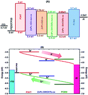
For better understanding of the effect of ZnPc-hybrids on the P3HT:PCBM blend, pristine P3HT was examined by forming blends with ZnPc-hybrids to study the effects of these hybrids on the main polymer. Full characterisation of the ZnPc-hybrids as well as description of energy level alignments (see Fig. 1(A)) have been carried out and results were published elsewhere.21 The energy levels alignment is assumed to be occurring between P3HT/ZnPc–rGO-non-co, P3HT/ZnPc–rGO-co, P3HT/ZnPc–SWCNTs-non-co and P3HT/ZnPc–SWCNTs-co. It is known that the main mechanisms in the OSCs operation are based on exciton generation, separation and dissociation with charge separation mainly taking place at the interface between the two materials (donor/acceptor) within the blends. No clear evidence of a junction may form at the interface between P3HT and ZnPc-hybrids since P3HT and ZnPc are known to behave as a p-type semiconductors22 while ZnPc carbon-based hybrids are also likely to act as p-type materials; in the literature it has been demonstrated that P3HT/SWCNTs hybrids can act as hole transport layers.23,24 Moreover, Fig. 1(B) shows the band bending diagram within the P3HT:PCBM:ZnPc–SWCNTs-co blend system as an example. In order to demonstrate the absence of a junction at the interface between P3HT and ZnPc hybrids, IV measurements have been performed on devices comprising P3HT and ZnPc hybrids; Fig. 1(C) shows symmetric IV characteristics for all studied devices.
image file: c6ra17590b-f1.tif
Fig. 1 (A) Energy level alignments for the materials under study, where only one of the ZnPc-hybrids is involved at a time; (B) proposed band bending diagram for the P3HT:PCBM:ZnPc–SWCNTs-co based device as an example for the energy levels position and the flow direction of both charge carriers; these energy levels were determined using cyclic voltammetry as discussed in our previous publication,21 and (C) IV characteristics for P3HT:ZnPc-hybrids-based devices.

Morphology studies of OSC active layers

Fig. 2 shows AFM images of P3HT:ZnPc-hybrid films which demonstrate noticeable changes in the surface morphology upon addition of ZnPc hybrids. These images demonstrate different dispersion for the different ZnPc hybrids within the P3HT matrix. Phase contrast analysis of the obtained AFM images has been carried out using WSxM software, and the phase images were analysed using Fast Fourier Transform (FFT) analysis. In order to increase the number of interfaces between two components in a blend, phase separation should be minimal. This leads to the improved dissociation rate of the photogenerated excitons at these interfaces. Qualitative analysis of AFM images of P3HT:ZnPc hybrids shows noticeable phase separation between the two components.25 The morphological features of P3HT:PCBM blends and P3HT:PCBM:ZnPc-hybrid blends have also been examined using SEM techniques. Fig. 3 shows SEM images of the ZnPc hybrid films as well as P3HT:PCBM active layers, both pure and blended with the ZnPc hybrids. All studied layers have exhibited nanoscale networks. ZnPc–SWCNTs-non-co films have shown clear SWCNT features while ZnPc–SWCNT-co films have exhibited different surface topography. On the other hand, rGO-based films have exhibited different morphologies which are attributed to the two dimensional nature of graphene itself. ZnPc:rGO-co hybrid has shown stacks-like features whereas ZnPc:rGO-non-co hybrid has exhibited flakes-like features.21 On blending these hybrids with P3HT:PCBM, clear features of SWCNTs have been observed in the case of ZnPc:SWCNTs-non-co compared to ZnPc:SWCNTs-co hybrid which suggests higher homogeneity in the case of covalently bonded hybrids. P3HT:PCBM blends involving rGO based hybrids have exhibited flakes-like features on the film surface.
image file: c6ra17590b-f2.tif
Fig. 2 AFM images of P3HT:ZnPc-hybrids based films with phase contrast and 2D-FFT analysis.

image file: c6ra17590b-f3.tif
Fig. 3 SEM images of ZnPc-hybrids and P3HT:PCBM:ZnPc-hybrids films.

Fig. 4 shows AFM images of hybrid films under study. P3HT:PCBM film has revealed a smooth surface with rms of 1.2 nm whereas introducing ZnPc: hybrids within P3HT:PCBM blends lead to rougher surface morphologies due to the nature of these hybrids as shown in the SEM images. P3HT:PCBM:ZnPc:SWCNTs-non-co blend has shown slightly higher surface roughness with rms value of about 2.35 nm whereas P3HT:PCBM:ZnPc:SWCNTs-co blend has exhibited a surface roughness rms of 2.3 nm. On the other hand, P3HT:PCBM:ZnPc:rGO-non-co and P3HT:PCBM:ZnPc:rGO-co blends have exhibited surface roughness of 2.4 nm and 2 nm, respectively. It could be claimed that the formation of rougher surface as a result of adding these hybrids to P3HT:PCBM blend could increase the contact area with the top electrode and therefore increases the current density and charge carrier collection.26 To compare the P3HT:PCBM:ZnPc with P3HT:ZnPc hybrids, phase contrast and 2D-FFT analyses of AFM images of their films have been carried out. A reduction of the phase separation between the P3HT:PCBM blends and the hybrids of ZnPc:rGO and ZnPc:SWCNT is observed because the 2D-FFT analysis shows an increase in the darker background on the image of P3HT:PCBM:ZnPc hybrids (Fig. 4) compared to P3HT:ZnPc hybrids based films (Fig. 2). Phase separation between P3HT:PCBM blend and rGO or SWCNT hybrids with ZnPc decreases leading to enhanced dissociation rate of the photogenerated excitons.25


image file: c6ra17590b-f4.tif
Fig. 4 AFM images of P3HT:PCBM:ZnPc-hybrids films with phase contrast and 2D-FFT analysis.

Optical properties

Fig. 5(a) shows the optical absorption spectra of P3HT:PCBM:ZnPc-hybrid layers under study. The absorption spectra for P3HT:PCBM blend are characterised by 3 absorption bands (A, B, and C) which are related to the P3HT absorption whereas the forth band (D) is related to absorption by PCBM molecules.27–29 The main absorption peak C (around λ = 510 nm) was attributed to the π–π* electronic transition in the P3HT polymer,30 whereas the two shoulders A and B (around 610 nm and 555 nm respectively) could be ascribed to the absorption of the extended conjugated P3HT and inter-chain stacking of P3HT respectively. This might suggest that an improved orientation as well as better chain packing of P3HT main polymer have developed within the blend.28 On the other hand, ZnPc material usually has two main bands, the Soret and the Q bands.31 Further details regarding the absorption spectra of the ZnPc-hybrids alone could be found in our previous publication.21 Fig. 5(b) shows the absorption spectra of P3HT:ZnPc-hybrids based solution; absorption spectra of these hybrids are mainly dominated by P3HT features being the main absorber in the blend. These spectra have exhibited significant absorption peak at around 450 nm which is ascribed to P3HT absorption.32 An additional absorption peak at around 300 nm was observed which might be ascribed to the interaction between P3HT and ZnPc-hybrids.33 Moreover, spectra of P3HT:ZnPc-hybrid films (Fig. 5(c)) give an indication of the π–π interactions within the P3HT:ZnPc-hybrids. A clear red shift in the absorption peak of P3HT from 450 nm in solutions to 550 nm in the films spectra and the occurrence of more distinct vibronic shoulders at around 600 nm and 500 nm suggest a more rigid structure of P3HT despite the presence of ZnPc-hybrids within the films' blend. The presence of ZnPc-hybrids within the blend however may have the advantage of enhancing light absorption by the hybrids which could lead to enhanced photo-generated carries due to the π–π interaction between ZnPc and rGO or SWCNTs.21 Salim and co-authors10 have argued that the slight increase in absorbance is thought to enhance the photon harvesting which may contribute to improved charge carrier generation.
image file: c6ra17590b-f5.tif
Fig. 5 (a) The absorption spectra of P3HT:PCBM:ZnPc-hybrids films; (b) absorption spectra of P3HT-hybrids solution samples; and (c) absorption spectra of P3HT-hybrid films samples.

Films' structural analysis

The structural properties for both P3HT:ZnPc-hybrids (Fig. 6(a)) and P3HT:PCBM:ZnPc-hybrids (Fig. 6(b)) thin layers were studied using XRD. Generally, P3HT chains facilitate their self-orientation into two-dimensional sheets by means of inter-chain stacking and hence demonstrate highly crystalline property.7 A single diffraction peak at 2θ = 5.5 ± 0.1° for (100) preferential orientation was observed in the case of P3HT:ZnPc-hybrids and ascribed to the edge-on orientation of the P3HT polymer; this corresponds to the in-plane π–π stacking of conjugated polymer rings and out of plane stacking of the alkyl groups perpendicular to the substrate, as depicted in Fig. 6(c). The reflection peak in all studied films is attributed to the P3HT lamellar structure, which suggests higher degree of crystallinity.34 No significant change in the crystallinity was detected due to the addition of a small amount of ZnPc-hybrids within the P3HT blend. However there seems to be a little change in the FWHM of the measured peak which might indicate a change of the crystallite sizes within the blend. Salim et al.10 have demonstrated that higher concentrations of SWCNTs disturb the orientation of P3HT, and the edge-on orientation partially changed into face-on orientation, as illustrated in Fig. 6(c). Therefore, a low concentration of the studied hybrids has been used in this work in order to avoid significant structural disorder as well as reducing chances of device short circuit occurrence. Similar diffraction peaks are observed in the case of P3HT:PCBM:ZnPc-hybrid films, and are attributed to the edge-on orientation of P3HT main polymer. The stacking distance of P3HT lamellar structure does not change with ZnPc-hybrids and PCBM contents; furthermore, the addition of ZnPc-hybrids did not change the amorphous morphology of PCBM.35
image file: c6ra17590b-f6.tif
Fig. 6 (a) XRD patterns of P3HT-hybrids films; (b) XRD patterns of P3HT:PCBM:ZnPc-hybrids films; and (c) orientation of P3HT.

Moreover, all the studied blend films were deposited from the solution in chlorobenzene[thin space (1/6-em)]:[thin space (1/6-em)]chloroform (CB[thin space (1/6-em)]:[thin space (1/6-em)]CF) mixture which enables slow drying process for the films and may assist in nanoscale interpenetrated networks formation.7 The presence of ZnPc hybrids within P3HT:PCBM shows no significant effect on the structural properties and the films remain showing almost same peak intensity of the same (100) orientation without observing any shifting or new peaks as shown in Fig. 6(b). This favourable orientation could assist in charge carrier transport by forming percolation pathways for both carriers, leading to higher solar cell performance.36

Films' electrical conductivity

DC electrical conductivity (σ) was determined for thin films of the studied blends using platinum interdigitated electrodes (IDE) as described elsewhere.37 The increase in conductivity from 0.07 to 2 mS m−1 as a result of adding ZnPc:SWCNTs-non-co to P3HT:PCBM blend compared to that of pristine P3HT:PCBM can be attributed to the well-distributed ZnPc-hybrids within the P3HT:PCBM blend as shown in the SEM and AFM images as well as the efficient charge transfer between the blend molecules.38,39 Moreover, the conductivity of P3HT:PCBM has increased to 6 mS m−1 as a results of adding ZnPc:SWCNTs-co to the blend as shown in Table 1. The significant increase in σ is thought to be the result of efficient charge transfer between ZnPc and SWCNTs or rGO hybrids, which suggests that nanoscale interpenetrated network has been achieved.21 This nanoscale structure as well as the improved charge transfer would also contribute in preventing charge carriers' recombination and thus improving the PCE of the OSCs.40 These improvements in active layers' electrical conduction could also contribute in enhancing the shunt resistance by creating percolation pathways which facilitate charge carriers' transport and increase the short circuit current density.20
Table 1 Electrical parameters for P3HT:PCBM and P3HT:PCBM:ZnPc-hybrids estimated from dark JV curves
Samples n Rs (Ω) µ × 10−6 (cm2 V−1 s−1) σ (mS m−1)
P3HT:PCBM 2.52 48.3 4.65 0.07
P3HT:PCBM:ZnPc:rGO-co 2.05 24.8 9.10 0.13
P3HT:PCBM:ZnPc:rGO-non-co 2.07 47.8 4.72 0.13
P3HT:PCBM:ZnPc:SWCNTs-co 1.99 24.8 9.34 6
P3HT:PCBM:ZnPc:SWCNTs-non-co 2.04 36.2 6.19 2


Dark current–voltage characteristics

Charge carrier mobility (µ), series resistance (Rs) as well as ideality factor (n) of the studied OSC devices have been evaluated using dark JV measurements and employing space charge limited conduction (SCLC) and thermionic emission theories; theoretical details of these analysis approaches are discussed elsewhere.41,42 Fig. 7(a) shows a plot of ln[thin space (1/6-em)]J versus applied voltage (V) for the studied devices. The ideality factor (n) is estimated using the following equation:43
 
image file: c6ra17590b-t1.tif(1)
where k is Boltzmann constant, q is the electron elementary charge, T is the absolute temperature and dV/dln[thin space (1/6-em)]J is the gradient of the linear part of the ln[thin space (1/6-em)]JV curves; the obtained values of n are summarised in Table 1. P3HT:PCBM reference device has exhibited higher recombination rate as indicated by the device ideality factor of 2.52. Diode parameters such as ideality factor and dark saturation current obtained from dark J(V) measurements were shown to be in agreement within experimental error with those derived using transient techniques for OSC based on P3HT:PCBM.44 The lowest ideality factor of 1.99 was obtained for P3HT:PCBM:ZnPc:SWCNTs-co based devices indicating the lowest recombination rate in these blends. The charge carrier mobility was estimated using a double log scale of the dark JV characteristics as shown in Fig. 7(b). Generally, all the curves have exhibited power law dependency of the form JVm, where m is the gradient of the log–log plot, which assumes different values over different applied voltage regions.45 Four distinct regions were demonstrated in the log[thin space (1/6-em)]J–log[thin space (1/6-em)]V curves; at low applied voltage where m ≈ 1, charge transport is governed by Ohm's law. At applied voltages in the range 0.2–0.3 V the slope has changed to approximately 2, where charge transport could be attributed to trap-controlled space charge limited conduction (SCLC) with traps located at a single energy level inside the band gap.42,46 The gradient becomes very steep at the applied voltages in the range at 0.45–0.65 V with m taking values between 9 and 12. This region of the log[thin space (1/6-em)]J–log[thin space (1/6-em)]V dependence can be related to trap-filling limit beyond which trap-filled SCLC mechanism occurs.46 The latter mechanism is evident by the onset of trap-free space charge limited conduction (TFCLC) with m taking on a value of ≈2 and the JV dependence is described by Child's law:47
 
image file: c6ra17590b-t2.tif(2)
where ε is the dielectric constant of the blend material, εo is the permittivity of free space, µ is the mobility and d is the device active layer thickness (150 nm). Using the data of the square law region (TFCLC) shown in Fig. 7(b) charge carrier mobility in the active layer can be estimated using eqn (2); obtained charge carrier mobility values are summarised in Table 1. The charge carrier mobility has nearly doubled in P3HT:PCBM:ZnPc–SWCNTs-co based device compared to P3HT:PCBM as a reference device. This increase in mobility could be attributed to the formation of percolation pathways, which facilitate the charge carrier transport through the blends. Furthermore, the series resistance was estimated from the slope at the high applied voltage as described previously.41 Its value has decreased from 48.3 Ω in P3HT:PCBM reference device to 24.8 Ω in the covalently bonded SWCNTs and rGO-based devices as shown in Table 1. Therefore, it could be assumed that the covalently bonded hybrids may contribute in higher current density and fill factor due to the lower Rs which in turn could give rise to higher device performance.48

image file: c6ra17590b-f7.tif
Fig. 7 Dark JV characteristics; (a) thermionic emission with ln(J)–V relation; (b) log[thin space (1/6-em)]J–log[thin space (1/6-em)]V for SCLC determination; and (c) solar cells characteristics of P3HT:PCBM and P3HT:PCBM:ZnPc-hybrids films.

Solar cell performance

P3HT:PCBM as well as P3HT:PCBM:ZnPc-hybrids solar cells have been investigated under illumination of 100 mW cm−2 and the JV characteristics of the hybrid OSCs are presented in Fig. 7(c). Solar cell devices prepared with P3HT:PCBM:ZnPc-hybrids as active layers have exhibited significantly improved power conversion efficiency (PCE) with values at least 36% higher in comparison with the reference P3HT:PCBM-based device as shown in Table 2. The highest performance was observed for P3HT:PCBM:ZnPc–SWCNTs-co based device with PCE of 5.3% and FF of 68%.
Table 2 Photovoltaic parameters of P3HT:PCBM and P3HT:PCBM:ZnPc-hybrids films
Samples Jsc (mA cm−2) Voc (V) FF PCE (%)
P3HT:PCBM 9.3 0.62 0.60 3.46
P3HT:PCBM:ZnPc:rGO-co 12 0.62 0.63 4.7
P3HT:PCBM:ZnPc:rGO-non-co 12 0.63 0.62 4.7
P3HT:PCBM:ZnPc:SWCNTs-co 12.6 0.62 0.68 5.3
P3HT:PCBM:ZnPc:SWCNTs-non-co 12 0.63 0.65 4.9


This increase in the device performance could be ascribed to the role of ZnPc-hybrids in inducing enhanced photon harvesting by the nanostructured P3HT:PCBM blends as well as improving charge carrier transport. The improved charge carrier transport could be attributed to the efficient charge transfer between the P3HT:PCBM and the ZnPc–SWCNTs-co hybrids within the new blends. The obtained higher FF could be ascribed to the lower recombination rate in these devices; FF represents the efficiency of charge collection before they recombine inside the cell, which basically depends on the charge carriers' mobility, Vbi and the charge carrier recombination rate.49 Furthermore, the obvious increase in the OSC's FF could be attributed to the improvement in the series resistance (Rs) as well as the reduced recombination rate as confirmed by the obtained lower value of diode ideality factor.50 Voc values have demonstrated no significant change in all studied devices as its value is mainly determined by the difference between the HOMOdonor and the LUMOacceptor as depicted by the following equation:51

 
Voc = [LUMOacceptor − HOMOdonor] − 0.3 (3)

The quantity of 0.3 V appearing in eqn (3) is the estimated loss of voltage, which might be attributed to the blend disorder that induces tail states or the energy loss induced by carriers' recombination.49 As revealed in Fig. 1(b), it could be said that electrons could easily be injected from the LUMO of PCBM to the respective electrode (Al) whereas the holes transfer takes place from the HOMO level of the P3HT or ZnPc-hybrids to the respective electrode which is the PEDOT:PSS/ITO front. This could be attributed to the difference in the work functions at the metal/organic semiconductor interface.52 It has also been shown that ZnPc-hybrids energy levels are located between the HOMO and the LUMO of both the donor and acceptor materials (see Fig. 1(b)). Several reports have demonstrated that changes in active layers' morphology are unlikely to have significant effect on the value of Voc.53,54 The enhancement in OSC device performance after doping P3HT:PCBM blends with ZnPc-hybrids could be ascribed to the enhancement in the electrical conductivity of the new blends as well as the increase in charge carriers' mobility which in turn improves short circuit current density. The effect of the distribution of ZnPc-hybrids within the P3HT:PCBM blend (nanoscale interpenetrated networks) as demonstrated by the morphological analysis could enhance the interface area within the blend, and thus result in improved charge carrier generation (larger Jsc) and charge transport (larger FF).55 Films of lower thickness of about 100 nm have been examined in line with our previous published work, where such thickness was shown to be an optimum active layer thickness that was associated with improved OSC performance.41 However, the thinner films have shown slightly smaller PCE but much improved FF. Such variations are likely to be associated with experimental artefacts and therefore more work is required in order to further illustrate the effect of active layer thickness. Stability of devices incorporating P3HT:PCBM blends with various nanocarbon materials functionalised with ZnPc will be a subject of future study using external quantum efficiency (EQE) measurements.

Experimental detail

Materials

Poly(3-hexathiophene-2,5-diyl) (P3HT), [6,6]-phenyl C61 butyric acid methyl ester (PCBM), poly(3,4-ethylenedioxythiophene)polystyrene sulfonate (PEDOT:PSS) 1.3 wt% dispersion in H2O (conductive grade), chlorobenzene (CB) and chloroform (CF) were all purchased from Sigma Aldrich and used without any further purification. ITO-coated glass slides (sheet resistant of 8–12 Ω sq.−1) were also purchased from Sigma Aldrich. The synthesis as well as the full characterisation of the zinc-phthalocyanine (ZnPc) covalently and non-covalently bonded to SWCNTs and rGO were described in the earlier study.21

P3HT:ZnPc hybrids preparation

Using chlorobenzene (CB) as solvent, P3HT-based hybrids have been prepared by mixing P3HT with ZnPc functionalised carbon nanomaterials (covalently (ZnPc-co) and ZnPc-non-covalently (ZnPc-non-co) bonded to SWCNTs or reduced graphene oxide (rGO)) in the weight ratio of (1[thin space (1/6-em)]:[thin space (1/6-em)]0.01) mg. The carbon nanomaterials were first dispersed in 1 mL CB and then P3HT was added to the suspension to produce the P3HT-based hybrids. These solutions were stirred overnight at 45 °C and were used to examine the effects of carbon-based functionalised ZnPc on the morphological, optical and structural properties of P3HT main polymer.

Organic solar cells fabrication

P3HT:PCBM blends were mixed with ZnPc functionalised carbon nanomaterials to produce a ternary active layer blends with the weight ratio of (1[thin space (1/6-em)]:[thin space (1/6-em)]1[thin space (1/6-em)]:[thin space (1/6-em)]0.01); these hybrids were dissolved in a co-solvent of CB and CF (1[thin space (1/6-em)]:[thin space (1/6-em)]1).56 The solutions were stirred overnight at 45 °C. ITO coated glass slides were cleaned using deionised water, acetone and 2-propanol for 10 min each in ultrasonic bath, respectively, and then blown dry in N2 gas. PEDOT:PSS layers were spin coated on the clean ITO substrates at 2000 rpm for 30 s, followed by heat-treatment at 150 °C for 10 min in ambient air. Subsequently, PEDOT:PSS layers coated ITO substrates were transferred to a nitrogen-filled glove box where the active layers were spin coated at 1500 rpm for 30 s to obtain a thickness of ∼150 nm and then heat-treated inside the glove box at 120 °C for 10 min. Aluminium (Al) was thermally evaporated as a back electrode using Edward thermal deposition system with a thickness of ∼100 nm under vacuum of ∼2 × 10⁻⁶ mbar, at the deposition rate of 0.1–0.2 nm s−1 as was detected by a quartz crystal thickness monitor. All completed devices were subjected to further heat-treatment inside the glove box at 120 °C for 10 min.

Characterization techniques

Thin films of P3HT-based hybrids, P3HT:PCBM blends and P3HT:PCBM:ZnPc functionalised carbon nanomaterial ternary blends were examined using UV-Visible spectroscopy (Varian 50-scan UV-Vis) in the range of 190–1100 nm. Thickness of the deposited layers was determined using M2000 (J.A. Woollam Co., Inc.) spectroscopic ellipsometer operating in the wavelength range 370–1000 nm. The structure properties of the studied layers were examined by multipurpose X'Pert Philips X-ray defractometer (MPD) (Cu, λ = 0.154 nm). The surface morphology was examined using FEI-Nova scanning electron microscope (SEM) as well as Nanoscope IIIa multimode atomic force microscope (Bruker-AFM). The photovoltaic properties in the form of current density–voltage (JV) dependence were measured using 4200 Keithley semiconductor characterisation system and the photo current was generated under AM 1.5 solar simulator source of 100 mW cm−2. The fill factor (FF) and the overall light to-electrical power conversion efficiency (PCE) of the solar cells were determined according to the following equations:57
 
image file: c6ra17590b-t3.tif(4)
 
image file: c6ra17590b-t4.tif(5)
where Jsc is the short-circuit current density (mA cm−2), Voc is the open-circuit voltage which is generally defined as the difference between the HOMOdonor and LUMOacceptor,50 Pin is the incident light power and Jmax (mA cm−2) and Vmax (V) are the current density and voltage at the point of maximum power output in the JV curves, respectively. The electrical conductivity was determined using DropSens interdigitated platinum electrodes (IDEs). The IDE can be used to measure the conductivity (σ) of the samples from the following relationship:41
 
image file: c6ra17590b-t5.tif(6)
where, t is the thickness of the film, W is the distance between the fingers (6.67 mm), n is the number of fingers (500), and (L) is the distance between the electrodes (5 µm).

Conclusions

In the current study, the effect of novel hybrids based on SWCNTs and rGO covalently and non-covalently functionalised ZnPc on the performance of organic solar cells based on P3HT:PCBM blend was investigated. The absorption spectra of P3HT:PCBM blend have shown no significant variation in the absorption peak positions as a result of the presence of these hybrids, however, ZnPc–rGO and ZnPc–SWCNTs hybrid features have appeared on the P3HT:PCBM surface morphology as verified by SEM and AFM images. Electrical properties of the studies blends have demonstrated significant improvement as a result of adding the ZnPc-functionalised hybrids. An increase of about two orders of magnitudes has been observed in the electrical conductivity associated with an increase in the charge carrier mobility with a reduction the ideality factor as well as a decrease in the series resistance, with the latter is thought to result in high FF. The solar cell devices based on P3HT:PCBM:ZnPc–SWCNTs-co bonded have demonstrated clear improvement in device performance with PCE = 5.3%, Jsc = 12.6 mA cm−2, Voc = 0.62 V and FF = 68%. A reference device based on bare P3HT:PCBM blend has exhibited PCE of just under 3.5%, Jsc of 9.3 mA cm−2, Voc of 0.62 V and FF of 60%.

Acknowledgements

Burak Kadem wishes to acknowledge the PhD scholarship awarded by the Ministry of Higher Education and Scientific Research in Iraq/Babylon University, Faculty of Science, Department of Physics.

References

  1. S. Günes, H. Neugebauer and N. S. Sariciftci, Chem. Rev., 2007, 107, 1324 CrossRef PubMed.
  2. Z. He, C. Zhong, S. Su, M. Xu, H. Wu and Y. Cao, Nat. Photonics, 2012, 6, 591 Search PubMed.
  3. S. N. Clafton, D. M. Huang, W. R. Massey and T. W. Kee, J. Phys. Chem. B, 2013, 117, 4626 CrossRef CAS PubMed.
  4. P. Roy, A. Jha and J. Dasgupta, Nanoscale, 2016, 8, 2768 RSC.
  5. J. A. Reinspach, Y. Diao, G. Giri, T. Sachse, K. England, Y. Zhou, C. Tassone, B. J. Worfolk, M. Presselt, M. F. Toney and S. Mannsfeld, ACS Appl. Mater. Interfaces, 2016, 8, 1742 CAS.
  6. D. Chalal, R. Garuz, D. Benachour, J. Bouclé and B. Ratier, Synth. Met., 2016, 212, 161 CrossRef CAS.
  7. Y. S. Kim, Y. Lee, J. K. Kim, E. O. Seo, E. W. Lee, W. Lee, S. H. Han and S. H. Lee, Curr. Appl. Phys., 2010, 10, 985 CrossRef.
  8. J. Liu, S. Shao, H. Wang, K. Zhao, L. Xue, X. Gao, Z. Xie and Y. Han, Org. Electron., 2010, 11, 775 CrossRef CAS.
  9. Y. Sun, J. Liu, Y. Ding and Y. Han, Colloids Surf., A, 2013, 421, 135 CrossRef CAS.
  10. T. Salim, H. W. Lee, L. H. Wong, J. H. Oh, Z. Bao and Y. M. Lam, Adv. Funct. Mater., 2016, 26, 51 CrossRef CAS.
  11. M. F. De Volder, S. H. Tawfick, R. H. Baughman and A. J. Hart, Science, 2013, 339, 535 CrossRef CAS PubMed.
  12. J. Wu, H. A. Becerril, Z. Bao, Z. Liu, Y. Chen and P. Peumans, Appl. Phys. Lett., 2008, 92, 263302 CrossRef.
  13. J. M. Yun, J. S. Yeo, J. Kim, H. G. Jeong, D. Y. Kim, Y. J. Noh, S. S. Kim, B. C. Ku and S. I. Na, Adv. Mater., 2011, 23, 4923 CrossRef CAS PubMed.
  14. Q. Liu, Z. Liu, X. Zhang, N. Zhang, L. Yang, S. Yin and Y. Chen, Appl. Phys. Lett., 2008, 92, 223303 CrossRef.
  15. H. Maruhashi, T. Oku, A. Suzuki, T. Akiyama and Y. Yamasaki, AIP Proceeding Conference Series, 2015, vol. 1649, p. 89 Search PubMed.
  16. U. Hahn, S. Engmann, C. Oelsner, C. Ehli, D. M. Guldi and T. Torres, J. Am. Chem. Soc., 2010, 132, 6392 CrossRef CAS PubMed.
  17. F. C. Moraes, D. L. Golinelli, L. H. Mascaro and S. A. Machado, Sens. Actuators, B, 2010, 148, 492 CrossRef CAS.
  18. N. Karousis, J. Ortiz, K. Ohkubo, T. Hasobe, S. Fukuzumi, A. Sastre-Santos and N. Tagmatarchis, J. Phys. Chem. C, 2012, 116, 20564 CAS.
  19. J. M. Holt, A. J. Ferguson, N. Kopidakis, B. A. Larsen, J. Bult, G. Rumbles and J. L. Blackburn, Nano Lett., 2010, 10, 4627 CrossRef CAS PubMed.
  20. H. Derbal-Habak, C. Bergeret, J. Cousseau and J. M. Nunzi, Sol. Energy Mater. Sol. Cells, 2011, 95, S53 CrossRef CAS.
  21. B. Kadem, M. Göksel, A. Şenocak, E. Demirbaş, D. Atilla, M. Durmuş, T. Basova, K. Shanmugasundaram and A. Hassan, Polyhedron, 2016, 110, 37 CrossRef CAS.
  22. A. Sarıyıldız, Ö. Vural, M. Evecen and Ş. Altındal, J. Mater. Sci.: Mater. Electron., 2014, 25, 4391 CrossRef.
  23. N. M. Dissanayake and Z. Zhong, Nano Lett., 2010, 11, 286 CrossRef PubMed.
  24. S. N. Habisreutinger, T. Leijtens, G. E. Eperon, S. D. Stranks, R. J. Nicholas and H. J. Snaith, Nano Lett., 2014, 14, 5561 CrossRef CAS PubMed.
  25. R. Bkakri, O. E. Kusmartseva, F. V. Kusmartsev, M. Song and A. Bouazizi, J. Lumin., 2015, 161, 264 CrossRef CAS.
  26. R. Geethu, C. S. Kartha and K. P. Vijayakumar, Sol. Energy, 2015, 120, 65 CrossRef CAS.
  27. B. Kadem and A. Hassan, Energy Procedia, 2015, 74, 439 CrossRef CAS.
  28. R. Ramani and S. Alam, Polymer, 2013, 54, 6785 CrossRef CAS.
  29. S. Cook, H. Ohkita, Y. Kim, J. J. Benson-Smith, D. D. Bradley and J. R. Durrant, Chem. Phys. Lett., 2007, 445, 276 CrossRef CAS.
  30. T. Erb, U. Zhokhavets, H. Hoppe, G. Gobsch, M. Al-Ibrahim and O. Ambacher, Thin Solid Films, 2006, 511, 483 CrossRef.
  31. M. N. Sibata, A. C. Tedesco and J. M. Marchetti, Eur. J. Pharm. Sci., 2004, 23, 131 CrossRef CAS PubMed.
  32. J. N. De Freitas, M. S. Maubane, G. Bepete, W. A. van Otterlo, N. J. Coville and A. F. Nogueira, Synth. Met., 2013, 176, 55 CrossRef CAS.
  33. H. Banimuslem, A. Hassan, T. Basova, M. Durmuş, S. Tuncel, A. A. Esenpınar, A. G. Gürek and V. Ahsen, J. Nanosci. Nanotechnol., 2015, 15, 2157 CrossRef CAS PubMed.
  34. J. H. Park, J. S. Kim, J. H. Lee, W. H. Lee and K. Cho, J. Phys. Chem. C, 2009, 113, 17579 CAS.
  35. E. D. Gomez, K. P. Barteau, H. Wang, M. F. Toney and Y. L. Loo, Chem. Commun., 2011, 47, 436 RSC.
  36. F. Reisdorffer, O. Haas, P. Le Rendu and T. P. Nguyen, Synth. Met., 2012, 161, 2544 CrossRef.
  37. B. Kadem, W. Cranton and A. Hassan, Org. Electron., 2015, 24, 73 CrossRef CAS.
  38. C. K. Najeeb, J. H. Lee, J. Chang and J. H. Kim, Nanotechnology, 2010, 21, 385302 CrossRef CAS PubMed.
  39. H. A. Alturaif, Z. A. ALOthman, J. G. Shapter and S. M. Wabaidur, Molecules, 2014, 19, 17329 CrossRef PubMed.
  40. P. Robaeys, F. Bonaccorso, E. Bourgeois, J. D'Haen, W. Dierckx, W. Dexters, D. Spoltore, J. Drijkoningen, J. Liesenborgs, A. Lombardo and A. C. Ferrari, Appl. Phys. Lett., 2014, 105, 083306 CrossRef.
  41. B. Kadem, A. Hassan and W. Cranton, 31st European Photovoltaic Solar Energy Conference and Exhibition, Germany-Hamburg, 2015, p. 1090 Search PubMed.
  42. B. Kadem, A. Hassan and W. Cranton, J. Mater. Sci.: Mater. Electron., 2016, 27, 7038 CrossRef CAS.
  43. Ö. Güllü, Ş. Aydoğan and A. Türüt, Solid State Commun., 2012, 152, 381 CrossRef.
  44. A. Foertig, J. Rauh, V. Dyakonov and C. Deibel, Phys. Rev. B: Condens. Matter Mater. Phys., 2012, 86, 115302 CrossRef.
  45. B. Gunduz, I. S. Yahia and F. Yakuphanoglu, Microelectron. Eng., 2012, 98, 41 CrossRef CAS.
  46. O. Oklobia and T. S. Shafai, Sol. Energy Mater. Sol. Cells, 2014, 122, 158 CrossRef CAS.
  47. D. H. Apaydın, D. E. Yıldız, A. Cirpan and L. Toppare, Sol. Energy Mater. Sol. Cells, 2013, 113, 100 CrossRef.
  48. W. Ma, C. Yang, X. Gong, K. Lee and A. J. Heeger, Adv. Funct. Mater., 2015, 15, 1617 CrossRef.
  49. B. Ray and M. A. Alam, Photovoltaic Specialists Conference IEEE 38th (PVSC), 2012, vol. 2, p. 1 Search PubMed.
  50. D. W. Zhao, A. K. K. Kyaw and X. W. Sun, Energy Efficiency and Renewable Energy Through Nanotechnology, Springer, London, 2011, p. 115 Search PubMed.
  51. B. Qi and J. Wang, J. Mater. Chem., 2012, 22, 24315 RSC.
  52. S. M. Sze and K. K. Ng, Physics of semiconductor devices, John Wiley & Sons, 2006 Search PubMed.
  53. B. Ray, M. S. Lundstrom and M. A. Alam, Appl. Phys. Lett., 2012, 100, 013307 CrossRef.
  54. B. Ray and M. A. Alam, Sol. Energy Mater. Sol. Cells, 2012, 99, 204 CrossRef CAS.
  55. I. Etxebarria, J. Ajuria and R. Pacios, Org. Electron., 2015, 19, 34 CrossRef CAS.
  56. B. Kadem, M. K. Al-Hashimi and A. Hassan, Energy Procedia, 2014, 50, 237 CrossRef CAS.
  57. G. Yue, J. Wu, Y. Xiao, H. Ye, J. Lin and M. Huang, Chin. Sci. Bull., 2011, 56, 325 CrossRef CAS.

This journal is © The Royal Society of Chemistry 2016
Click here to see how this site uses Cookies. View our privacy policy here.