
Spatial control of direct chemical vapor deposition of graphene on silicon dioxide by directional copper dewetting†
Wesley T. E. van den Beld*,
Albert van den Berg and
Jan C. T. Eijkel
BIOS – Lab on a Chip Group, MESA+ Institute for Nanotechnology, MIRA Institute for Biomedical Engineering and Technical Medicine, University of Twente, The Netherlands. E-mail: w.t.e.vandenbeld@utwente.nl; Tel: +31 53 489 5653
First published on 7th September 2016
Abstract
In this paper we present a method for the spatial control of direct graphene synthesis onto silicon dioxide by controlled dewetting. The dewetting process is controlled through a combination of using a grooved substrate and conducting copper deposition at an angle. The substrate is then treated using a typical graphene chemical vapor deposition synthesis process at an elevated temperature during which directional dewetting of the copper into the grooves occurs while graphene is deposited at the mesas in between the grooves. The dewetting process and the synthesized graphene layer are characterized. The method is a non-manual, controllable and wafer-scale process, and therefore opens new possibilities for the construction of functional devices such as e.g. transistors.
Since its discovery in 2004 as a functional material, there has been consistent growth in interest for graphene, owing to its unique electronic and mechanical properties.1–5 For most practical devices, such as transistors, it is essential to be able to synthesize a single layer of graphene on a dielectric surface.4,6,7 The first method successfully used to isolate a single layer of graphene was exfoliation of highly ordered pyrolytic graphite (HOPG) on silicon dioxide.8 Although this method results in high quality graphene, it is labor intensive, offers only a low yield and is therefore not useful for mass production. Another route to isolate graphene is by dissolving graphite in an oxidizing solution in combination with a drying procedure.9–11 Such chemical methods typically result in a large spread in the number of graphene layers.12 As an alternative, chemical vapor deposition (CVD) processes enable large area single layer graphene production. Usually, transition metals (copper, nickel, etc.) are used as catalysts for the decomposition of gaseous alkanes (methane, ethane).13 To release the CVD graphene from the metal substrate however, a manual transfer protocol is required, which makes the process again labor intensive and hard to automate. Therefore a direct synthesis process on dielectric substrates is seen to be crucial for the future of integration of graphene into practical devices. Metal-free graphene synthesis directly on insulators has also been shown to be possible, however these metal-free methods are typically accompanied by very long synthesis times caused by very low reaction rates compared to methods that make use of copper and nickel catalysts.14–16 The feasibility of graphene synthesis on copper oxide where copper oxide is also the catalytic material has been demonstrated.17 However, the electrical properties of copper oxide make it unsuitable for application in devices.18 Other research has shown that direct graphene synthesis is possible by dewetting of thin copper films on silica substrates using a CVD protocol.19 A disadvantage of this route is that dewetting copper on a flat substrate results in a randomly distributed patchy graphene pattern.19–23 Furthermore, the remaining copper particles will not fully evaporate, even after a long annealing time.19,21 When very long process times are used, the remaining copper particles can eventually even sink into the silica substrate.24
In this paper we report a solution for this random copper dewetting consisting of an improved method for direct and controlled graphene synthesis on silicon dioxide using controlled dewetting and evaporation of copper. The dewetting process is controlled by a combination of using a grooved substrate and conducting copper deposition at an angle. Areas for graphene deposition are defined as mesas in between grooves produced using a potassium hydroxide (KOH) wet etching process on a silicon substrate. Subsequently the wafer is oxidized to form a layer of silicon dioxide (SiO2), and a layer of copper (Cu) is deposited on the wafer. There are several advantages of using a grooved substrate over e.g., copper strips. The copper dewets in a single direction which is defined by the copper deposition angle, making it possible to deposit a single graphene line on the mesa. In addition, minimal copper oxidation occurs, since the last step prior to graphene synthesis is the deposition of copper enabling a proper catalytic surface for graphene deposition. In this research copper was chosen because of its excellent graphene synthesis catalytic properties, low carbon solubility and dewetting properties.19,22,25 For CVD graphene synthesis on thin copper films a lower temperature is required compared to copper foils.26 During the CVD process, graphene is continuously deposited directly onto the silicon dioxide mesa (the flat area between the grooves as displayed in Fig. 1a) while the copper is evaporating and dewetting into the silicon dioxide grooves.19,22 The quality of the deposited graphene which stays directly on the silicon dioxide has been optimized by varying the partial pressures of the reactive gasses in the CVD process. The method does not require graphene transfer and therefore opens new ways for the implementation of automated wafer-scale graphene synthesis.
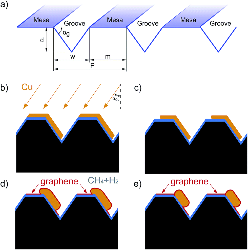 | ||
| Fig. 1 Design of the substrate with groove width w and mesa width m which repeat in period P (a). The groove is etched at an angle αg resulting in a groove depth d. Schematic of the method: copper deposition at an angle on the silicon dioxide/silicon substrate (b), conformation of the copper to the contact angle during heating (c), propagation of the contact line by dewetting and evaporation of the copper during the CVD process leaving a graphene layer (d) and the final situation with copper in the groove and the mesa covered by graphene (e). | ||
The design of the fabricated grooved substrate is shown in Fig. 1a. The mesa widths m range from 1 μm to 10 μm and the groove width w is set to m/0.4. The groove angle αg is determined by the silicon 〈100〉 crystal orientation as 54.7°. The silicon substrate was oxidized, resulting in a silicon dioxide layer of 300 nm serving as a copper diffusion barrier. Subsequently copper and graphene were deposited as schematically shown in Fig. 1. The copper is deposited on the substrate at an angle αCu by e-beam evaporation. This results in a copper thickness on the mesa of h = h0![[thin space (1/6-em)]](https://www.rsc.org/images/entities/char_2009.gif) cos(αCu), where the deposition thickness h0 is set to 500 nm. Subsequently, the substrate is treated by a CVD process at a temperature of 1000 °C. In this process the copper conforms initially to the copper silicon dioxide contact angle, followed by dewetting which is driven by the gradient of the curvature in the copper landscape.27,28 During this dewetting process, graphene is synthesized and left on the silicon dioxide surface by the retreating copper.19,27–29 Three phenomena can be observed in the dewetting process: conformation to the contact angle, propagation of the contact line and occasional film punch-through.
cos(αCu), where the deposition thickness h0 is set to 500 nm. Subsequently, the substrate is treated by a CVD process at a temperature of 1000 °C. In this process the copper conforms initially to the copper silicon dioxide contact angle, followed by dewetting which is driven by the gradient of the curvature in the copper landscape.27,28 During this dewetting process, graphene is synthesized and left on the silicon dioxide surface by the retreating copper.19,27–29 Three phenomena can be observed in the dewetting process: conformation to the contact angle, propagation of the contact line and occasional film punch-through.
Firstly, to minimize surface energy, a fast rearrangement at the edge of the film will occur in the initial stage until the contact angle θc is obtained.30 This contact angle of the dewetted copper with the surface can be calculated using Young’s equation
|
γi + γmcosθc = γs
| (1) |
The interface energy γi at the copper–silicon dioxide interface is 1.1 J m−2, the surface energy of copper γm is 1.3 J m−2 and the silicon dioxide surface energy γs is about 0.3 J m−2 close to the melting temperature of copper (1083 °C), resulting in a contact angle of approximately 128°.31,32
Secondly, after the fast initial conformation, copper evaporation and dewetting drive the propagation of the contact line.30,33 The dewetting transport is dominated by surface diffusion of the copper (bulk transport can be neglected), minimizing the surface chemical potential and therefore smoothing the film over time.30,34,35 The gradient of the curvature K over the surface landscape s leads to a metal flux Jm (assuming an isotropic surface energy) according to:28
 | (2) |
 where Na is Avogadro’s constant. For copper in a hydrogen environment at 1.0 mbar the surface diffusion pre-exponential is D0 = 1 × 10⁻⁵ m2 s−1 and the activation energy is Qs = 92 kJ mol−1.36 The temperature dependence of this surface diffusion allows tuning of the retraction velocity of the contact line. For metal films on flat substrates, the contact line will propagate as a function of time in the form of xcl ∼ tαdw, where αdw is dependent on geometrical film assumptions.37 In most studies an αdw-factor of about
  is found, which is practically independent of the contact angle.30,37,38 The mechanism for graphene deposition proposed by Ismach et al.19 is that graphene is synthesized by the catalytic action of the copper. While the contact line is retracting, graphene is transferred from the copper to the silicon dioxide surface, resulting in an insulating surface covered by graphene.
The deposited copper film is conformal and will have a constant curvature at the mesa-groove corner prior to dewetting (see Fig. 2a). To reduce the overall curvature of the copper surface, a dewetting flux will drive copper away from the mesa-groove corner as follows from eqn (2), resulting in local flattening of the surface.34,39 This process leads to a thinning of the copper film, eventually leading to a punch-through of the copper film by the mesa-groove corner.
 | ||
| Fig. 2 False colored SEM images of a cross section of the grooved substrate with 300 nm of silicon dioxide (blue) with 500 nm of copper (orange) deposited at 35° prior to (a) and after the chemical vapor process showing full dewetting (b), partial dewetting (c) and punch-through (d) with mesa widths of 3.0 μm, 4.1 μm and 5.0 μm, respectively. | ||
To determine the copper–silicon dioxide contact angle, a copper film of 500 nm was deposited on a flat substrate and processed using CVD at 1000 °C. Using scanning electron microscopy (SEM) a contact angle of 131° ± 4° was measured, which is in agreement with the theoretical contact angle.
Subsequently, controlled dewetting on a grooved substrate was tested by depositing copper and applying the graphene CVD protocol. Three regimes could be distinguished in the resulting structures: fully dewetted, partially dewetted and punched-through, as can be observed in Fig. 2. In the case of full dewetting, the copper has retracted into the groove. On the mesa (and in the groove) a layer of graphene was found to be deposited. Wider mesas became partially dewetted, with fingers of copper still remaining on the mesa. For even wider mesas punch-through of the copper film at the mesa-groove corner occurs, resulting in a roll of copper remaining on the mesa.
The effect of a wafer cleaning procedure prior to copper deposition was investigated by testing the following procedures: 5 min UV-ozone, 5 min oxygen plasma, directly from an oxidation oven and no pre-clean. No significant influence from this pre-cleaning protocol on the dewetted mesa area was found.
To further control directional dewetting, copper was deposited at an angle on the grooved substrate. A series of deposition angles αCu were tested to investigate their effect on the dewetted mesa area (see the ESI† for optical microscopy data). By image analysis of the dewetted surface, the relative dewetted mesa areas as a function of the mesa width and deposition angle were measured as shown in Fig. 3a. To the measurement data a logistic function was fitted in the form of
 | (3) |
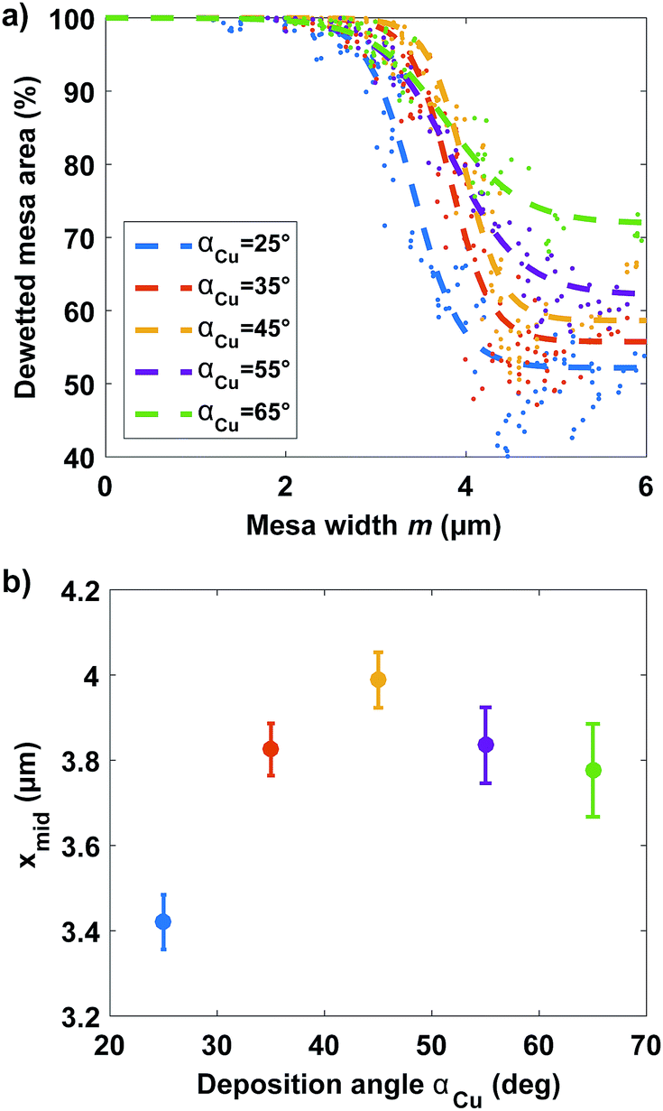 | ||
| Fig. 3 The resulting dewetted mesa areas as a function of the total mesa width m for a series of deposition angles αCu (a), where the copper deposition thickness h0 is set to 500 nm. To this measurement data a logistic function is fitted. A dewetted mesa area of 100% corresponds to a fully dewetted mesa. The fit variable mmid of the logistic fit function (see eqn (3)) versus the copper deposition angle (b), showing an optimal deposition angle of 45°, the error bars show 95% fit confidence bounds. | ||
To optimize the quality of the deposited graphene, several methods were tested in which hydrogen and methane gas flows were varied. The total gas inflow was set to 800 sccm using argon. The process pressure was set to 10 mbar to prevent too fast an evaporation of copper.33 The Raman spectra of the deposited graphene were subsequently recorded using a 532 nm laser. The graphene spectrum shows three characteristic peaks: the D peak (1350 cm−1) which indicates defects and discontinuities (e.g. crystal boundaries) in the graphene crystal, the G peak (1590 cm−1) which probes the in-plane bond stretching mode and the 2D peak (2700 cm−1) which holds information regarding the stacking orders.40,41 To analyze the measured Raman spectra, Lorentzian peaks were fitted to the mapped Raman scan. A sharp (low FWHM) and symmetric 2D peak indicates single layer graphene.40 Ideally no defects are present, thus the D peak intensity when normalized to the G peak intensity (ID/IG) should be low. Fewer graphene layers result in a higher G peak position,41,42 however doping will also increase this position.43
A series of methods for graphene deposition were tested and the Raman spectroscopy fitting results can be found in the ESI.† The four most significant graphene quality indicators displayed are indicators for the number of layers and the defect density (including grain size). In this process we aim to produce defect free, single layer graphene. When analyzing the graphene quality indicators discussed above, the method using 50 sccm methane and 50 sccm hydrogen was selected for subsequent graphene deposition experiments.
The spatial distribution of the graphene quality was analyzed and can be found in Fig. 4. Where the copper dewetting started, first no graphene was deposited. This is related to the high temperature required to synthesize graphene, which is not yet reached when the copper starts dewetting. From this point on, the presence of a continuous layer of graphene was confirmed using Raman spectroscopy. The first deposited graphene layer possesses a higher D peak compared to the rest of the mesa. We expect variation in the dewetting velocity to influence the quality of the deposited graphene. The dewetting velocity can be influenced by, for example, the process temperature. We therefore believe that it is possible to improve the graphene quality further by tuning the dewetting velocity. A more constant dewetting velocity is expected to result in a more uniform graphene layer. This could be achieved by an increase in the temperature or a decrease in the pressure during the deposition process. By slightly increasing the temperature during the process the dewetting velocity will also increase. Increasing the process pressure will reduce the evaporation rate of copper which would lead to an increase in the graphene domain size. Lastly, the quality of the deposited graphene could be improved by further optimization of the hydrogen, methane and argon gas flow in the synthesis method. The impact of decreasing the dewetting velocity is expected to be beneficial for the synthesis process. It could help in the synthesis of a continuous graphene layer with a lower defect density and an increased graphene domain size. Furthermore, less copper residues are expected at the expense of higher silicon oxide roughness.
 | ||
| Fig. 4 Characterization of the deposited graphene on the mesa area, using the best CVD settings (hydrogen at 50 sccm and methane at 50 sccm). Raman spectra were recorded on the mesa (light blue) as indicated by the red box on the optical image, scale bar is 10 μm (a). The colored crosses mark the locations of the displayed three Raman spectra (d). The dashed lines indicate the mesa edge in the mapped Raman scans, which reveal the graphene coverage on the mesa (b, c, e, f). The apparent noise in the right most spectrum (pink) is caused by the copper next to the mesa (d). The 2D to G peak intensity I2D/IG shows uniform quality over the sample (b). The D to G peak intensity ID/IG reveals more defects on the left edge of the mesa, where the copper dewetting had started (c). The 2D peak sharpness is uniform over the sample, however next to the mesa the 2D peak is sharper (e). The G peak position is higher on the mesa than next to the mesa (suspended and on copper), which is probably caused by the difference in the substrate induced doping (f). | ||
After close inspection, SEM images revealed ridging in the silicon dioxide as can be seen in Fig. 5. By atomic force microscopy (AFM) the ridges were measured to have an average amplitude of 4 nm and a period of 47 nm (see the ESI† for AFM data). The forming of ridges during the copper dewetting process is explained by the transport of silicon dioxide along the interface with copper to the triple point where process gasses, copper, and silicon dioxide meet. The silicon dioxide is then transported by surface diffusion, which is inherent to metal ceramic systems at elevated temperatures.24,44–46
 | ||
| Fig. 5 False colored SEM image of the grooved substrate showing the fully dewetted mesa surface with silicon dioxide (blue) and the dewetted copper (orange). On the mesa surface, ridges and graphene are found which are both formed during copper dewetting in the CVD process. | ||
In the study by Ismach et al.19 these ridges were also observed, however it was suggested that these ridges were wrinkles in the graphene. To confirm that the ridges in this work are in the silicon dioxide and not caused by e.g. graphene wrinkles, the sample was treated using oxygen plasma to strip the graphene. AFM images before and after this treatment showed a comparable roughness, from which we conclude that the silicon dioxide was ridged during the dewetting process. The continuity of the graphene layer was investigated using hydrofluoric acid (HF) treatment, since the graphene layer will protect the silicon dioxide against etching. After etching, the roughness was found to be comparable to the original sample, confirming that the graphene layer is continuous. In the AFM images nanoparticles of approximately 24 nm were observed on the sample surface. Analysis with an energy selective backscattered (EsB) detector and by energy-dispersive X-ray spectroscopy (EDX) showed that these nanoparticles are copper particles which must have been pinched off during the dewetting process (see the ESI† for EsB data). The particles are most probably completely wrapped up in graphene.47 Interesting plasmonic properties have been reported in the literature, when these graphene coated copper particles spaced or have features in the order of tens of nanometers.48–50 The graphene coating protected the copper from oxidation while it increased the sensitivity of measurements of analyte adsorption on the graphene.50–52 Removal of these copper residues would be possible by subsequent wet etching of the copper, since this removes the copper particles and leaves the graphene supported by the substrate,53 where the etchant is thought to reach the copper via the defects in the graphene.
The deposited graphene could be used as a transistor channel, which was demonstrated by the construction of a device in which the graphene can be gated. The synthesized graphene was interfaced with gold electrodes and a well was made with epoxy resin which served as a reservoir for an electrolyte solution. By solution gating a high gate capacitance is achieved, inducing high doping levels.43,54 In Fig. 6 the rectifying behavior of the graphene as a function of gating voltage is shown, which is normally not present in single layer graphene field effect transistor devices.55 The curve we found indicates the presence of a band gap in the graphene,56 which is useful for transistor devices.
 | ||
| Fig. 6 The graphene in-plane conductance as a function of the gating voltage. The gating voltage was applied using a silver/silver chloride electrode in a 0.1 M potassium chloride solution. The length of the error bars represent two standard deviation units of the measurement. | ||
In addition to this, the synthesized graphene could be exploited for other functional devices such as (bio)sensors, since the synthesized graphene layer consists of relatively small grains (nanocrystalline19) and therefore possesses a relative high density of reactive grain boundaries. Another potential application for this graphene deposition method, after further optimization, would be the fabrication of graphene nanoribbons.
In summary, the presented method has improved the direct synthesis process of graphene on silicon dioxide by controlling the location of the dewetted areas. For this purpose copper was deposited at an angle on a grooved substrate. The copper dewetted into the grooves, leaving a layer of graphene on the flat part of the silicon dioxide surface. Optimization of the CVD process has been performed to obtain the best synthesized graphene sample possible. Furthermore analysis showed that the graphene layer is closed and the silicon dioxide surface was ridged after the dewetting process. This improved method opens new possibilities for wafer-scale graphene synthesis directly on insulating surfaces.
Experimental section
An oxidized 〈100〉 silicon wafer was patterned using conventional lithography with a line mask of 400 lines ranging from 1 μm to 10 μm in width. After performing dry etching of the silicon dioxide, silicon was wet-etched anisotropically using a 25% KOH solution at 75 °C to manufacture the grooves. Because of the crystal orientation of the wafer, a groove angle αg of 54.7° is obtained. Subsequently, the grooved substrate was oxidized resulting in a silicon dioxide layer of 300 nm for optimal graphene visualization and to serve as a copper barrier at higher temperatures. Next, 500 nm of copper was deposited using e-beam evaporation at a controlled angle. Directly after this, the CVD process was performed in a cold-wall reaction chamber, which was purged with hydrogen prior to starting the process. Meanwhile, as the substrate was heated to 1000 °C (ramping up and down at ∼60°C min−1), the CVD-process was executed at a pressure of 10 mbar with a hydrogen flow of 50 sccm, a methane flow of 50 sccm and an argon flow of 700 sccm for 15 minutes, see the ESI† for the CVD log data. The Raman spectra are recorded using a WITec alpha 300 system with a 532 nm laser at 1 mW using a 100× objective (0.9 NA) leading to a spot size of . For the fabrication of the graphene transistor device, gold contact pads were deposited by electron beam evaporation using a shadow mask, and were connected to a PCB by wire bonding. Subsequently, the gold pads and wire bonds were covered with epoxy (hysol), leaving the graphene area between the electrodes (5 mm) open. A droplet of 0.1 M KCl solution was applied to this area in which a silver/silver chloride electrode was inserted. Between the gold pads a voltage of 0.1 V was applied to measure the in-plane conductance. The graphene was solution gated by connecting the silver/silver chloride electrode to a Biologic SP300 potentiostat.
Acknowledgements
Financial support from Spinoza Grant for Albert van den Berg is acknowledged. This work was also supported by the Netherlands Center for Multiscale Catalytic Energy Conversion (MCEC), and an NWO Gravitation programme funded by the Ministry of Education, Culture and Science of the government of the Netherlands. Furthermore, the assistance of J. T. Loessberg-Zahl, H. Le The, J. G. M. Sanderink, J. W. Mertens and G. P. M. Roelofs is gratefully acknowledged.References
- M. I. Katsnelson, Mater. Today, 2007, 10, 20–27 CrossRef CAS.
- K. Geim and K. S. Novoselov, Nat. Mater., 2007, 6, 183–191 CrossRef PubMed.
- K. Novoselov, Z. Jiang, Y. Zhang, S. Morozov, H. Stormer, U. Zeitler, J. Maan, G. Boebinger, P. Kim and A. Geim, Science, 2007, 315, 1379 CrossRef CAS PubMed.
- J. Bunch, S. Verbridge, J. Alden, A. Van Der Zande, J. Parpia, H. Craighead and P. McEuen, Nano Lett., 2008, 8, 2458–2462 CrossRef CAS PubMed.
- Y. Zhu, S. Murali, W. Cai, X. Li, J. Suk, J. Potts and R. Ruoff, Adv. Mater., 2010, 22, 3906–3924 CrossRef CAS PubMed.
- N. Lei, P. Li, W. Xue and J. Xu, Meas. Sci. Technol., 2011, 22, 107002 CrossRef.
- F. Yan, M. Zhang and J. Li, Adv. Healthcare Mater., 2014, 3, 313–331 CrossRef CAS PubMed.
- K. S. Novoselov, A. K. Geim, S. Morozov, D. Jiang, Y. Zhang, S. Dubonos, I. Grigorieva and A. Firsov, Science, 2004, 306, 666–669 CrossRef CAS PubMed.
- V. C. Tung, M. J. Allen, Y. Yang and R. B. Kaner, Nat. Nanotechnol., 2009, 4, 25–29 CrossRef CAS PubMed.
- B. Cai, S. Wang, L. Huang, Y. Ning, Z. Zhang and G.-J. Zhang, ACS Nano, 2014, 8, 2632–2638 CrossRef CAS PubMed.
- S. Gilje, S. Han, M. Wang, K. L. Wang and R. B. Kaner, Nano Lett., 2007, 7, 3394–3398 CrossRef CAS PubMed.
- Z.-S. Wu, W. Ren, L. Gao, B. Liu, C. Jiang and H.-M. Cheng, Carbon, 2009, 47, 493–499 CrossRef CAS.
- R. Muñoz and C. Gómez-Aleixandre, Chem. Vap. Deposition, 2013, 19, 297–322 CrossRef.
- J. Sun, T. Gao, X. Song, Y. Zhao, Y. Lin, H. Wang, D. Ma, Y. Chen, W. Xiang and J. Wang, et al., J. Am. Chem. Soc., 2014, 136, 6574–6577 CrossRef CAS PubMed.
- J. Sun, Y. Chen, M. K. Priydarshi, Z. Chen, A. Bachmatiuk, Z. Zou, Z. Chen, X. Song, Y. Gao and M. H. Rümmeli, et al., Nano Lett., 2015, 15, 5846–5854 CrossRef CAS PubMed.
- J. Chen, Y. Wen, Y. Guo, B. Wu, L. Huang, Y. Xue, D. Geng, D. Wang, G. Yu and Y. Liu, J. Am. Chem. Soc., 2011, 133, 17548–17551 CrossRef CAS PubMed.
- S. Gottardi, K. Müller, L. Bignardi, J. C. Moreno-López, T. A. Pham, O. Ivashenko, M. Yablonskikh, A. Barinov, J. Björk and P. Rudolf, Nano Lett., 2015, 15, 917–922 CrossRef CAS PubMed.
- A. Smith and H. Wieder, J. Phys. Chem., 1959, 63, 2013–2015 CrossRef CAS.
- A. Ismach, C. Druzgalski, S. Penwell, A. Schwartzberg, M. Zheng, A. Javey, J. Bokor and Y. Zhang, Nano Lett., 2010, 10, 1542–1548 CrossRef CAS PubMed.
- E. Jiran and C. Thompson, Thin Solid Films, 1992, 208, 23–28 CrossRef CAS.
- C. M. Müller and R. Spolenak, J. Appl. Phys., 2013, 113, 094301 CrossRef.
- L. Croin, E. Vittone and G. Amato, Thin Solid Films, 2014, 573, 122–127 CrossRef CAS.
- T. Kaplas, D. Sharma and Y. Svirko, Carbon, 2012, 50, 1503–1509 CrossRef CAS.
- L. J. de Vreede, A. van den Berg and J. C. Eijkel, Nano Lett., 2015, 15, 727–731 CrossRef CAS PubMed.
- S. Bhaviripudi, X. Jia, M. S. Dresselhaus and J. Kong, Nano Lett., 2010, 10, 4128–4133 CrossRef CAS PubMed.
- L. Tao, J. Lee, H. Chou, M. Holt, R. S. Ruoff and D. Akinwande, ACS Nano, 2012, 6, 2319–2325 CrossRef CAS PubMed.
- C. V. Thompson, Annu. Rev. Mater. Res., 2012, 42, 399–434 CrossRef CAS.
- W. W. Mullins, J. Appl. Phys., 1957, 28, 333–339 CrossRef CAS.
- D. Wang, R. Ji and P. Schaaf, Beilstein J. Nanotechnol., 2011, 2, 318–326 CrossRef CAS PubMed.
- H. Wong, P. Voorhees, M. Miksis and S. Davis, Acta Mater., 2000, 48, 1719–1728 CrossRef CAS.
- C. J. Smithells and E. A. Brandes, Metals reference book, London etc, Butterworth, 1976 Search PubMed.
- J.-Y. Kwon, T.-S. Yoon, K.-B. Kim and S.-H. Min, J. Appl. Phys., 2003, 93, 3270–3278 CrossRef CAS.
- G. Meng, T. Yanagida, M. Kanai, M. Suzuki, K. Nagashima, B. Xu, F. Zhuge, A. Klamchuen, Y. He and S. Rahong, Phys. Rev. E, 2013, 87, 012405 CrossRef PubMed.
- A. Giermann and C. Thompson, J. Appl. Phys., 2011, 109, 083520 CrossRef.
- D. Srolovitz and S. Safran, J. Appl. Phys., 1986, 60, 255–260 CrossRef CAS.
- F. Bradshaw, R. Brandon and C. Wheeler, Acta Metall., 1964, 12, 1057–1063 CrossRef CAS.
- F. Cheynis, F. Leroy and P. Müller, C. R. Phys., 2013, 14, 578–589 CrossRef CAS.
- A. Presland, G. Price and D. Trimm, Prog. Surf. Sci., 1972, 3, 63–96 CrossRef CAS.
- W. W. Mullins, J. Appl. Phys., 1959, 30, 77–83 CrossRef.
- A. Ferrari, J. Meyer, V. Scardaci, C. Casiraghi, M. Lazzeri, F. Mauri, S. Piscanec, D. Jiang, K. Novoselov and S. Roth, Phys. Rev. Lett., 2006, 97, 187401 CrossRef CAS PubMed.
- L. Malard, M. Pimenta, G. Dresselhaus and M. Dresselhaus, Phys. Rep., 2009, 473, 51–87 CrossRef CAS.
- A. C. Ferrari, Solid State Commun., 2007, 143, 47–57 CrossRef CAS.
- A. Das, S. Pisana, B. Chakraborty, S. Piscanec, S. Saha, U. Waghmare, K. Novoselov, H. Krishnamurthy, A. Geim and A. Ferrari, Nat. Nanotechnol., 2008, 3, 210–215 CrossRef CAS PubMed.
- E. Saiz, A. Tomsia and R. Cannon, Acta Mater., 1998, 46, 2349–2361 CrossRef CAS.
- E. Saiz, R. M. Cannon and A. P. Tomsia, Oil Gas Sci. Technol., 2001, 56, 89–96 CAS.
- W. D. Kaplan, D. Chatain, P. Wynblatt and W. C. Carter, J. Mater. Sci., 2013, 48, 5681–5717 CrossRef CAS.
- M. Fuentes-Cabrera, B. H. Rhodes, J. D. Fowlkes, A. López-Benzanilla, H. Terrones, M. L. Simpson and P. D. Rack, Phys. Rev. E, 2011, 83, 041603 CrossRef PubMed.
- D. Ansell, I. Radko, Z. Han, F. Rodriguez, S. Bozhevolnyi and A. Grigorenko, Nat. commun., 2015, 6, 8846 CrossRef CAS PubMed.
- X. Li, X. Ren, Y. Zhang, W. C. Choy and B. Wei, Nanoscale, 2015, 7, 11291–11299 RSC.
- X. Zhang, S. Xu, S. Jiang, J. Wang, J. Wei, S. Xu, S. Gao, H. Liu, H. Qiu and Z. Li, et al., Appl. Surf. Sci., 2015, 353, 63–70 CrossRef CAS.
- Y. Zhao, G. Chen, Y. Du, J. Xu, S. Wu, Y. Qu and Y. Zhu, Nanoscale, 2014, 6, 13754–13760 RSC.
- V. Kravets, R. Jalil, Y.-J. Kim, D. Ansell, D. Aznakayeva, B. Thackray, L. Britnell, B. Belle, F. Withers and I. Radko, et al., Sci. Rep., 2014, 4, 5517 CAS.
- C.-Y. Su, D. Fu, A.-Y. Lu, K.-K. Liu, Y. Xu, Z.-Y. Juang and L.-J. Li, Nanotechnology, 2011, 22, 185309 CrossRef PubMed.
- J.-H. Zhong, J.-Y. Liu, Q. Li, M.-G. Li, Z.-C. Zeng, S. Hu, D.-Y. Wu, W. Cai and B. Ren, Electrochim. Acta, 2013, 110, 754–761 CrossRef CAS.
- T.-Y. Chen, P. T. K. Loan, C.-L. Hsu, Y.-H. Lee, J. Tse-Wei Wang, K.-H. Wei, C.-T. Lin and L.-J. Li, Biosens. Bioelectron., 2013, 41, 103–109 CrossRef CAS PubMed.
- J. Park, W. C. Mitchel, S. Elhamri, L. Grazulis, J. Hoelscher, K. Mahalingam, C. Hwang, S.-K. Mo and J. Lee, Nat. commun., 2015, 5677 CrossRef CAS PubMed.
Footnote |
| † Electronic supplementary information (ESI) available: Optical microscopy data of dewetted mesas, Raman spectroscopy analysis results of deposited graphene, atomic force microscopy data of ridges on mesas, energy selective backscatter data of copper nanoparticles and CVD log data. See DOI: 10.1039/c6ra16935j |
| This journal is © The Royal Society of Chemistry 2016 |