
 Open Access Article
 This Open Access Article is licensed under a
 Creative Commons Attribution 3.0 Unported Licence
Carbon nanotube–silicon heterojunction solar cells with surface-textured Si and solution-processed carbon nanotube films†
Eri Muramotoa,
Yuhei Yamasakia,
Feijiu Wangb,
Kei Hasegawaa,
Kazunari Matsudab and
Suguru Noda*a
aDepartment of Applied Chemistry, Waseda University, 3-4-1 Okubo, Shinjuku-ku, Tokyo 169-8555, Japan. E-mail: noda@waseda.jp
bInstitute of Advanced Energy, Kyoto University, Uji, Kyoto 611-0011, Japan
First published on 26th September 2016
Abstract
Carbon nanotube (CNT)–silicon (Si) heterojunction solar cells are fabricated with surface-textured Si substrates. Using a dilute alkaline solution, common etchant in the Si solar cell industry, we formed a pyramidal texture on the Si substrate surface. The texture effectively enhances the absorption of the incident light, improving the short-circuit current density by ∼1.3-fold, up to 33.1 mA cm−2. We fabricated CNT–Si solar cells with a power conversion efficiency (PCE) of 10.4% without any anti-reflective coatings or doping of the CNTs. Moreover, the CNT films were prepared from commercialized CNT agglomerates by a mild solution-based process, which is well suited for the fabrication of CNT–Si solar cells with large area. We also achieved a PCE of 9.57% for a flat cell with careful removal of surfactant from and doping by nitric acid of the CNT films. These findings suggest that with the combination of surface-textured Si and solution-processed CNT films, efficient and low-cost CNT–Si solar cells may be realized.
Introduction
Solar cells harness the sun's free and inexhaustible energy without emitting any green house gases upon operation. Although combinations with other renewables are necessary to tackle today's global issues such as energy security and mitigation of climate change, solar cells have many advantages such as modularity that allows installation in distributed locations or locations with limited area. Innumerable materials and device structures have been researched to further improve the quality and decrease the manufacturing cost but the bulk single-crystalline and multi-crystalline silicon (Si) solar cells still dominate the market (market share > 90%)1 owing to their low price, high power conversion efficiency (PCE) and durability. Simpler fabrication of Si-based solar cells is a promising approach to reduce the cost of photovoltaics (PVs) further.In the past decade, a novel type whose junction is fabricated by a fast and simple process of attaching carbon nanotube (CNT) film to Si wafer was reported.2,3 The progress has been summarized in several reviews.4–6 Wei et al. synthesized spider webs of double-wall CNTs by floating catalyst chemical vapor deposition (FCCVD), removed catalysts from the webs by HNO3 and HCl treatments, transferred the webs to n-type Si (n-Si) substrates and obtained PCE of 1.38% in 2007.2 They soon improved the PCE to 7.4% and reported the importance of removing native oxide layer from the Si substrates.3 PCEs higher than 10% were then achieved with special films of single-wall CNTs (SWCNTs). Cui et al. reported a 10.0% PCE using hexagonal frames of SWCNTs with HNO3 doping.7 They synthesized vertically aligned SWCNT arrays on catalyst-supported substrates by CVD, transformed the arrays into hexagonal frames by H2O vapor treatment, and transferred the frames from the growth substrates to n-Si substrates using hot water. Li et al. reported a 11.5% PCE using horizontally aligned SWCNT films fabricated by superacid slide casting method.8 They prepared an ink of SWCNTs from SouthWest Nanotechnology by vigorously stirring them in chlorosulfonic acid for three days, sandwiching the ink with two glass slides where it is spread and sheared, floating on water and transferring the SWCNT films to n-Si substrates. Wang et al. further improved the performance to 12.5% and 14.5% without and with HNO3-doping of the SWCNT films, which were synthesized by FCCVD, captured on membrane filters, and dry-transferred to n-Si substrates.9 Recently Harris et al. prepared SWCNT films by a method similar to that by Li et al.,8 examined the effects of horizontal alignment and chirality sorting of SWCNTs, and obtained the PCE as high as 13.5% with randomly aligned, unsorted SWCNT films with doping.10 Nicola et al. reported a 10 ± 1% PCE using multi-wall CNTs from Nanocyl and the importance of removal of surfactant used for MWCNT dispersion.11 In this way, high PCE values were initially obtained only with specially prepared SWCNT films, but more recently, also with regular CNT films.
Different materials have been extensively studied for doping and anti-reflection. It is popular to form heterojunction of n-Si with CNTs doped in p-type; chemical treatments using HNO3,7,12 HNO3 with AuCl3,8 H2O2,13 SOCl2,14 and SOCl2 with AuCl3 (ref. 10) have been reported. In addition, heterojunctions of both p-CNTs/n-Si and n-CNTs/p-Si using metallocenes15 as well as electronic junction control by electrolyte gate using ionic liquid16 have been reported. Anti-reflective coating, such by TiO2,17 polymethyl methacrylate,18,19 and other polymers19 also improved the PV performance. The record PCE of 17.0% was realized with the combined use of dry-transferred SWCNT films and MoOx overlayer, which has both effects of anti-reflection and p-doping of the CNT films.20 So far, significant progress has been made in the past decade in CNT–Si heterojunction solar cells. However, it is important to obtain better PV performance with simpler fabrication process, and more efforts can be made on the Si substrates.
In this paper, we investigated the effect of surface texturing of the Si. There has been a debate on the role of CNTs in this type of solar cells but recent analyses have shown that much of the carriers that contribute to power generation seem to be produced in the Si layer.21–24 Shu et al. reported hybrid heterojunction and photoelectrochemistry solar cells based on silicon nanowires, which enhance the light absorption.25,26 We herein integrated chemical etching of semiconducting materials, which has been studied for a long time,27 into the CNT–Si solar cells. In the industry today, crystalline Si wafers are anisotropically etched by a dilute alkaline solution to reduce the reflection losses from the front surface of silicon solar cells.28,29 We formed micro-size pyramids on the CNT/Si active window using a dilute sodium hydroxide (NaOH) solution. The pyramids effectively absorbed the incident light and improved the PV performance of the CNT–Si solar cells. We evaluated the solar cells carefully by precisely controlling the light illumination area, and average and best efficiencies of 7.21% and 8.21% without texture and 9.87% and 10.4% with texture were achieved without any extra anti-reflective coatings or doping of the CNTs. Moreover, CNT–Si heterojunction was realized in such cells using the CNT films fabricated by a mild solution-based process. We found that thoroughly removing surfactant residue in the CNT films using hot water is critically important to achieve good PV performance.
Furthermore, the findings in this study can be used to fabricate thin-film CNT–Si solar cells. There is a growing demand for film solar cells, which are lightweight, flexible and well suited for building-integrated installations. The layer transfer method or ribbon process30–32 produce large-grain polycrystalline Si films with a thickness of ∼100 μm by crystallizing molten Si. Recently, we have developed the “rapid vapor deposition of liquid Si and in situ melt crystallization” process, which realized large-grain (>100 μm), 10 μm-thick continuous polycrystalline films within 1 min.33 Our ultimate goal is to fabricate flexible, thin film CNT–Si solar cells.
Experimental
CNT thin films were prepared from a dilute CNT dispersion by vacuum filtration. 1–3 mg of CNT agglomerates produced by FCCVD34 (MEIJO eDIPS, EC grade; Meijo Nano Carbon Co., Ltd., Nagoya, Japan) were dispersed in 30 mL of 0.5 wt% aqueous solution of sodium dodecylbenzenesulfonate (SDBS, Sigma Aldrich, St. Louis, MO, USA) by bath sonication (VS-50R, VELVO-CLEAR, Tokyo, Japan) at 30 W and 45 kHz for 3 min.35 The liquid was centrifuged at 2700 rpm for 40 min, and 15 mL of the supernatant was separated. Then 15 mL of 0.5 wt% SDBS aqueous solution was added to the remaining portion. This dispersion and centrifugation procedure was repeated 4 times, and the separated supernatant was diluted with 0.5 wt% SDBS aqueous solution to perform two-fold dilution. Several hundred microliters of the dispersion and 15 mL of purified water were vacuum filtrated onto a hydrophilic membrane filter (pore size 0.1 μm, VCWP, Merck Millipore, Darmstadt, Germany), to form a thin CNT film. The membrane filter was slowly immersed into purified water to let the CNT film detach and float on the water. The amount of CNT dispersion was changed to obtain films with the targeted optical transmittance values.The Si surface was textured using a dilute alkaline solution. An n-Si(100) substrate (1–5 Ω cm with P as dopant) covered by 500 nm SiO2 layer with a circular opening (ϕ = 2 mm) was treated by 2 wt% NaOH in 20 vol% isopropanol (IPA)/H2O solution at 75–80 °C for 30 min under reflux. The substrates were washed thoroughly with purified H2O. The textured Si surfaces with and without CNT films were observed using a scanning electron microscope (SEM, Hitachi S-4800, Tokyo, Japan).
The prepared CNT film was transferred onto a Si substrate and dried in thermostatic chamber at 100 °C for 3 min. The native oxide layer on the Si window was removed by etching in 4.7 wt% HF aq for 30 s and rinsed in IPA and purified water. A top Au anode with 2.1 mm-sized opening (square or circle) was formed on the CNT film by sputtering and a bottom In cathode was formed by welding its wire to n-Si with its native oxide layer scraped off (Fig. 1a). In some cells, to dope the CNT film,36 a drop of 1 M HNO3 was placed on the Si window for 2 min and then removed by a pipette.
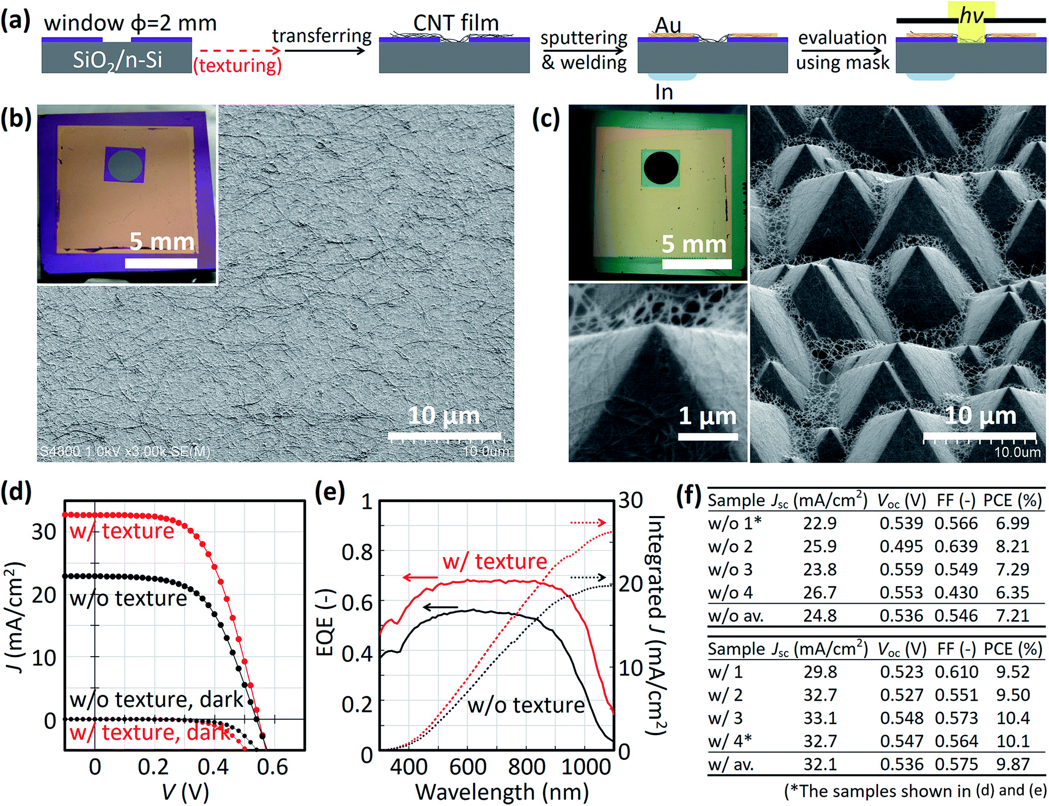 | ||
| Fig. 1 Fabrication process, structure, and PV performance of the typical CNT–Si solar cells. (a) Cell fabrication and PV performance evaluation processes. (b and c) Tilted surface-view SEM images of CNT–Si solar cells without (b) and with (c) Si surface textures. Insets show optical images and a high magnification SEM image of the cells. (d) Current density (J)–voltage (V) curves, (e) EQE and integrated J vs. wavelength, and (f) PV performances of the cells without any anti-reflective coatings or doping of the CNTs. CNT films were washed with hot water before drying and then transferred to the Si substrates. | ||
Solar cells were evaluated using the solar cell evaluation system (JASCO YQ-2000, Tokyo, Japan) under 1 sun illumination (Pinput = 100 mW cm−2, AM1.5G). A light-blocking mask of 10 × 10 mm2-sized 50 μm-thick Ni foil with a hole (ϕ = 2 mm) was placed on the solar cell during evaluation to standardize the amount of incident light. The thin SiO2 and Au layers partially transmit the incident light to the n-Si where extra carriers are produced and may contribute to the power generation. We therefore used the mask and determined PCE values to avoid over-valuation of PV performance. The Ni-foil mask was covered with an insulating tape to avoid short-circuit.
Results and discussion
CNT–Si solar cells without and with surface texture
We first investigated the effect of Si surface texturing on the PV performance of the CNT–Si solar cells (Fig. 1). CNT films with optical transmittance T = 90% at 550 nm wavelength were used in this experiment. The solar cell with a CNT film on the flat Si surface appears bright because the incident light is not well absorbed (inset of Fig. 1b). The CNTs make a network structure on the flat Si(100) surface (Fig. 1b). On the other hand, as the dark surface depicts, the NaOH-treated Si efficiently absorbs the incident light (top inset of Fig. 1c). This is because the incident light is reflected multiple times by the several-μm-pitch pyramids formed by 4 stable (111) faces (Fig. 1c). Significant difference in the reflectivity was confirmed by an ultraviolet-visible (UV-Vis) spectrophotometer; 37.4% and 11.5% at a wavelength of 550 nm for flat (without texture) and textured Si surfaces with CNT films (see Fig. S1†). The CNT film attaches well to the top halves of the pyramid surfaces, and hanging at the valleys (bottom inset of Fig. 1c). The CNT–Si solar cell with textured Si showed an average short-circuit current density (Jsc) of 32.1 mA cm−2, which is a ∼1.3-fold increase from the value with the Si without texture (24.8 mA cm−2, Fig. 1d and f). The external quantum efficiency (EQE) reached almost 0.7, which is approximately a 0.2 improvement from the Si without texture in the wavelength range of 500–800 nm (Fig. 1e). The integrated current density calculated using the AM1.5G spectrum and the EQE data (wavelength range of 300–1100 nm) was 19.8 mA cm−2 and 26.3 mA cm−2 for the cells without and with texture, respectively, which were somewhat smaller than the directly measured values. Fig. 1f shows the variations in the PV performance of the CNT–Si solar cells (see Fig. S2† for the J–V curves). Overall, the PCE improved substantially, to 9.87% on average and 10.4% for the best cell, which is ∼1.3 times higher than the original values of 7.21% and 8.21%. It should be noted that such PV performances were achieved without any anti-reflective coatings or doping of the CNTs. Easy formation of CNT–Si heterojunction was possible with solution-processed CNT films even for textured Si surfaces owing to the flexible nature of the CNT films.However, such good PV performances were achieved only when the CNT films were washed carefully before making the cells. Even the cells with Si surface texture showed low average values of Voc (0.450 V), FF (0.438) and PCE (6.32%) when CNT films were used as-filtrated (see Fig. S3† for the J–V curves).
Effect of surfactant removal on the PV performance of CNT–Si solar cells
We then investigated the effect of removing surfactant (SDBS) from the CNT films on the PV performance. We used flat Si substrates to observe only the effects of CNT post-treatments. We tried four different post-treatments for the CNT films (T = 90%) after detaching from the membrane filters as shown in Fig. 2. As a reference, one solar cell with a pristine CNT film (without post-treatment) was also prepared (Fig. 2a). One CNT film was washed before drying by heating and holding the water, on which an as-filtrated film floated, at 95–98 °C for 70 min (Fig. 2b). Two other CNT films were dried on a Si substrate (Fig. 2c) or kanthal ring (Fig. 2d). The CNT film dried on Si substrate was then washed by dropping hot water on it continuously for 70 min while keeping the Si substrate at the same temperature. On the other hand, the CNT film dried on kanthal ring was placed in water, which was heated and held at 95–98 °C for 70 min. The fifth CNT film was dried on a kanthal ring and annealed at 600 °C for 60 min under 10 vol% H2/Ar at 1 atm (Fig. 2e).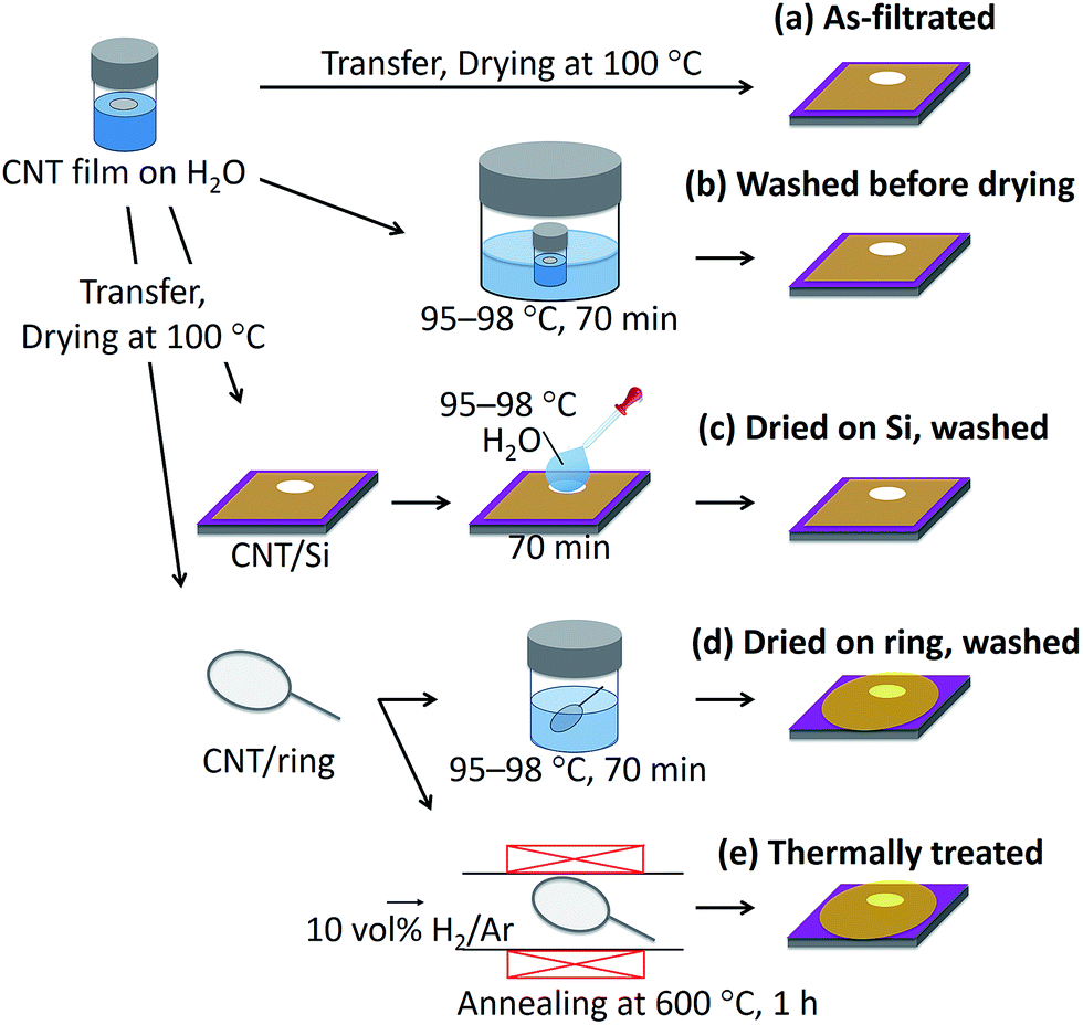 | ||
| Fig. 2 Schematic of CNT–Si solar cell fabrication process with different treatments for surfactant removal from CNT films. | ||
For each CNT–Si solar cell described above, we evaluated the PV performance before and after the treatment with 1 M HNO3.36 Washing before drying improved the Jsc from 24.4 to 26.3 mA cm−2, and fill factor (FF) from 0.37 to 0.52, respectively (Fig. 3a and b). As a result, the PCE increased from 4.76% to 7.16%, which is a 1.5-fold increase. A treatment of the film with HNO3 further improved the FF to 0.63 and the open-circuit voltage (Voc) to 0.58 V, resulting in the highest PCE of 9.57% (Fig. 3b). The HNO3 treatment did not improve the PV performance for the cell without washing (Fig. 3a), showing that washing with water is necessary to obtain the high PCE. This is possibly because the washing process removes the residual SDBS which can act as carrier recombination centers. The HNO3 treatment dopes the CNTs36 and possibly removes SDBS further from the film.
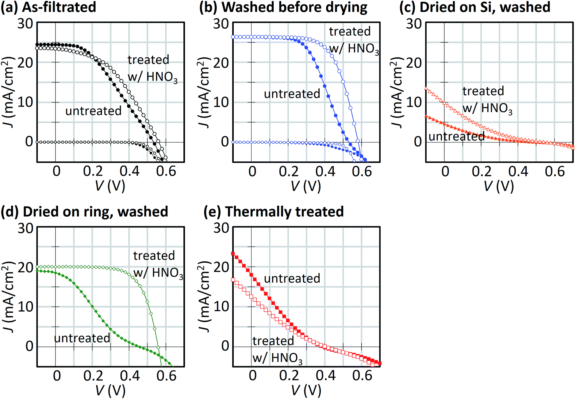 | ||
| Fig. 3 J–V characteristics of flat CNT–Si solar cells fabricated with different treatments for surfactant removal from CNT films. | ||
When the CNT film was dried on Si and then washed with water, the PV performance was considerably poor (Fig. 3c). Only a slight increase of Jsc was observed after HNO3 treatment. In contrast, despite the low FF of the as-made CNT–Si solar cell with CNT film dried on the kanthal ring and washed with water, HNO3 treatment significantly improved the Jsc, Voc, and FF values, resulting in a high PCE of 7.29% (Fig. 3d). This is a 5% improvement from the original value (Fig. 3d). This improvement comes from p-doping of and possible further SDBS removal from the CNTs. The Jsc is smaller than that of the cell with a CNT film washed before drying (Fig. 3b) because the CNT film was unavoidably wrinkled during washing on the kanthal ring, resulting in reduced optical transmittance and/or poorer contact to the Si surface. Furthermore, the CNT–Si solar cell with a CNT film dried on Si showed a much poorer performance than that with a CNT film dried on kanthal ring (Fig. 3c and d). This is presumably because the SDBS molecules from the as-filtrated film attached strongly to and condensed on Si surface during washing-drying. The CNT–Si solar cell with the annealed CNT film also showed a very poor performance (Fig. 3e). Some residue of thermally decomposed SDBS may also trap carriers. The results are summarized in Table 1.
| Sample | Jsc (mA cm−2) | Voc (V) | FF (−) | PCE (%) |
|---|---|---|---|---|
| (a) As-filtrated | 24.4 → 23.3 | 0.53 → 0.56 | 0.37 → 0.43 | 4.76 → 5.62 |
| (b) Washed before drying | 26.3 → 26.3 | 0.53 → 0.58 | 0.52 → 0.63 | 7.16 → 9.57 |
| (c) Dried on Si, washed | 4.64 → 9.90 | 0.52 → 0.56 | 0.15 → 0.15 | 0.35 → 0.82 |
| (d) Dried on ring, washed | 18.5 → 20.0 | 0.45 → 0.56 | 0.25 → 0.65 | 2.10 → 7.29 |
| (e) Annealed | 18.0 → 12.6 | 0.39 → 0.40 | 0.20 → 0.20 | 1.38 → 0.99 |
As it seems that the SDBS residue considerably affect the PV performance, we analyzed the differently-treated CNT films by contact angle measurement of water droplets. The as-filtrated CNT film showed the smallest contact angle of 87°, which means it is the most hydrophilic (Fig. 4a). On the other hand, the CNT film washed before drying showed the largest contact angle of 118°, which means it is the most hydrophobic (Fig. 4b). The CNT film dried on Si and washed showed the medium contact angle of 101° (Fig. 4c). Since surfactants make CNT films hydrophilic, these results suggest that the CNT film washed before drying has the smallest amount of surfactants. Thorough removal of surfactants from the CNTs and/or Si becomes more difficult once the film is dried.
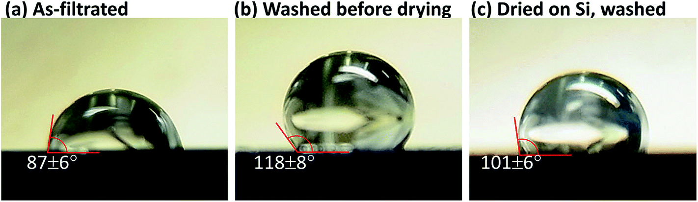 | ||
| Fig. 4 Contact angle measurement of water droplets on differently-treated CNT films on flat Si substrates. The errors in the contact angles are the standard deviation for 10–12 droplets (see Fig. S4† for details). | ||
We also applied Fourier transform infrared spectroscopy (FT-IR), Raman spectroscopy and X-ray photoelectron spectroscopy (XPS) (Fig. S5–S7†). None of the functional groups could be detected from the CNT films by either FT-IR or Raman, possibly because the SDBS residue was too small. By XPS, a weak Na peak was detected for the as-filtrated CNT film whereas no Na peak was detected for the film washed before drying (ESI Fig. S7†). These results suggest that hot water washes away SDBS and Na in particular, which can trap carriers and act as carrier recombination centers. As a result, the best PV performance was obtained with the CNT film that was washed before drying (Fig. 2b). HNO3 treatment p-dopes CNTs, which enhances their hole extraction ability, and may further remove the impurity residue.
PV performance of CNT–Si cells using CNT film with different optical transmittance
We now discuss the effect of optical transmittance of CNT films on the PV performance. We prepared and compared the CNT films having the optical transmittance (wavelength 550 nm) of 71.9%, 79.8%, and 88.7% (called T = 70%, 80%, 90%, respectively, hereafter) with sheet resistances of 42.0 Ω sq−1, 55.4 Ω sq−1, and 268 Ω sq−1, respectively (see Fig. S8† for the details). The PV performances are shown in Fig. 5 and Table 2. The CNT–Si solar cell with the CNT film of T = 90% showed the greatest PV performance with an overall PCE of 9.57%. The highest Jsc of 26.3 mA cm−2 was obtained with T = 90% owing to the largest light absorption by the n-Si. In contrast, the highest Voc of 0.593 V was obtained with T = 80% and a lower Voc of 0.565 V was obtained with T = 70%. This difference can possibly be attributed to the different recombination rates within the CNT film or at the Si surface. Removing impurities from the thicker film (T = 70%) may be more difficult than removing them from thinner films. The FF of the CNT–Si solar cell with T = 80% film was the highest and that of the cell with T = 70% film was the lowest. The thinnest CNT film of T = 90% has a high sheet resistance with large series resistance while the thickest CNT film of T = 70% possibly has a large impurity with small shunt resistance.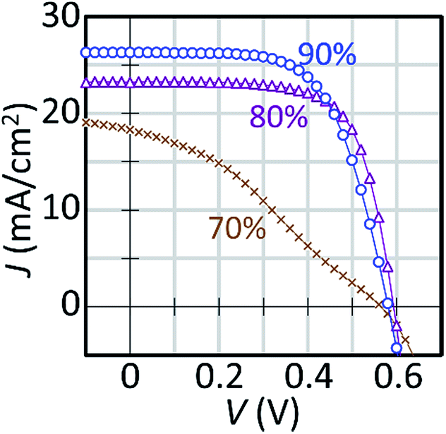 | ||
| Fig. 5 J–V curves of flat CNT–Si solar cells with CNT films of different optical transmittances. The cells were treated with HNO3. | ||
| Sample | Jsc (mA cm−2) | Voc (V) | FF (−) | PCE (%) |
|---|---|---|---|---|
| T = 70% | 18.3 | 0.565 | 0.321 | 3.32 |
| T = 80% | 23.2 | 0.593 | 0.690 | 9.50 |
| T = 90% | 26.3 | 0.581 | 0.627 | 9.57 |
As explained above, surface texturing of the Si substrates, careful removal of surfactant from the CNT films, and p-doping of the CNT films are effective in enhancing the PCE of the CNT–Si cells. The full combination of these technologies, however, resulted in a poor performance possibly due to the excess HNO3 residue on textured Si surfaces. Effective doping of CNT films on textured Si substrates is now under study.
Conclusions
We fabricated CNT–Si solar cells by combining the textured Si and CNT films prepared by solution-based process. We formed pyramidal texture on the Si with a dilute alkaline solution, and confirmed that it effectively absorbs the incident light. The Jsc and EQE both increased by ∼1.3-times, resulting in a ∼1.3-times higher PCE. The PCE of 10.4% for the best cell without any anti-reflective coatings or chemical doping of the CNTs was achieved just by texturing the Si surface. We also examined the effect of post-treatments to remove the surfactant SDBS from the solution-processed CNT films on PV performances, using flat Si substrates. Washing the CNT film with hot water before drying was found to improve the PV performance significantly, achieving the highest PCE of 9.57%. The measurement of wettability of the CNT films showed that the washing process removes the SDBS residue that presumably acts as carrier recombination centers. Careful application of the existing technologies, such as texturing of Si surface, dispersion-coating of CNTs, and removal of surfactant, will make CNT–Si solar cells more practical with improved productivity and PV performance.Acknowledgements
We would like to thank Prof. Nishide, Prof. Oyaizu, and Ms. Nakajima at Department of Applied Chemistry, Waseda University for their support in J–V measurements, Mr Enomoto at Kagami Memorial Research Institute for Materials Science and Technology, Waseda University for XPS measurements, Meijo Nano Carbon Co., Ltd. for providing us with their MEIJO eDIPS CNTs, and Dr Sugime at Waseda Institute for Advanced Study, Waseda University for his help in editing this manuscript. This work was financially supported by JSPS KAKENHI Grant Numbers 15K14216 and 25107002, and by the ALCA, JST.Notes and references
- G. Bye and B. Ceccaroli, Sol. Energy Mater. Sol. Cells, 2014, 130, 634–646 CrossRef CAS.
- J. Wei, Y. Jia, Q. Shu, Z. Gu, K. Wang, D. Zhuang, G. Zhang, Z. Wang, J. Luo and A. Cao, Nano Lett., 2007, 7, 2317–2321 CrossRef CAS PubMed.
- Y. Jia, J. Wei, K. Wang, A. Cao, Q. Shu, X. Gui, Y. Zhu, D. Zhuang, G. Zhang, B. Ma, L. Wang, W. Liu, Z. Wang, J. Luo and D. Wu, Adv. Mater., 2008, 20, 4594–4598 CrossRef CAS.
- D. D. Tune, B. S. Flavel, R. Krupke and J. G. Shapter, Adv. Energy Mater., 2012, 2, 1043–1055 CrossRef CAS.
- J. Di, X. Wang, Y. Xing, Y. Zhang, X. Zhang, W. Lu, Q. Li and Y. T. Zhu, Small, 2014, 10, 4606–4625 CrossRef CAS PubMed.
- X. Li, Z. Lv and H. Zhu, Adv. Mater., 2015, 27, 6549–6574 CrossRef CAS PubMed.
- K. Cui, T. Chiba, S. Omiya, T. Thurakitseree, P. Zhao, S. Fujii, H. Kataura, E. Einarsson, S. Chiashi and S. Maruyama, J. Phys. Chem. Lett., 2013, 4, 2571–2576 CrossRef CAS.
- X. Li, Y. Jung, K. Sakimoto, T. H. Goh, M. A. Reed and A. D. Taylor, Energy Environ. Sci., 2013, 6, 879–887 CAS.
- F. Wang, D. Kozawa, Y. Miyauchi, K. Hiraoka, S. Mouri, Y. Ohno and K. Matsuda, ACS Photonics, 2014, 1, 360–364 CrossRef CAS.
- J. M. Harris, R. J. Headrick, M. R. Semler, J. A. Fagan, M. Pasquali and E. K. Hobbie, Nanoscale, 2016, 8, 7969–7977 RSC.
- F. De Nicola, M. Salvato, C. Cirillo, M. Crivellari, M. Boscardin, M. Scarselli, F. Nanni, I. Cacciotti, M. De Crescenzi and P. Castrucci, Carbon, 2016, 101, 226–234 CrossRef CAS.
- Y. Jia, A. Cao, X. Bai, Z. Li, L. Zhang, N. Guo, J. Wei, K. Wang, H. Zhu, D. Wu and P. M. Ajayan, Nano Lett., 2011, 11, 1901–1905 CrossRef CAS PubMed.
- X. Bai, H. Wang, J. Wei, Y. Jia, H. Zhu, K. Wang and D. Wu, Chem. Phys. Lett., 2012, 533, 70–73 CrossRef CAS.
- Z. Li, V. P. Kunets, V. Saini, Y. Xu, E. Dervishi, G. J. Salamo, A. R. Biris and A. S. Biris, Appl. Phys. Lett., 2008, 93, 243117 CrossRef.
- X. Li, L. M. Guard, J. Jiang, K. Sakimoto, J. S. Huang, J. Wu, J. Li, L. Yu, R. Pokhrel, G. W. Brudvig, S. Ismail-Beigi, N. Hazari and A. D. Taylor, Nano Lett., 2014, 14, 3388–3394 CrossRef CAS PubMed.
- P. Wadhwa, B. Liu, M. A. McCarthy, Z. Wu and A. G. Rinzler, Nano Lett., 2010, 10, 5001–5005 CrossRef CAS PubMed.
- E. Shi, L. Zhang, Z. Li, P. Li, Y. Shang, Y. Jia, J. Wei, K. Wang, H. Zhu, D. Wu, S. Zhang and A. Cao, Sci. Rep., 2012, 2, 884–888 Search PubMed.
- R. Li, J. Di, Z. Yong, B. Sun and Q. Li, J. Mater. Chem. A, 2014, 2, 4140–4143 CAS.
- L. Yu, D. D. Tune, C. J. Shearer and J. G. Shapter, Sol. Energy, 2015, 118, 592–599 CrossRef CAS.
- F. Wang, D. Kozawa, Y. Miyauchi, K. Hiraoka, S. Mouri, Y. Ohno and K. Matsuda, Nat. Commun., 2015, 6, 6305–6312 CrossRef CAS PubMed.
- P. L. Ong, W. B. Euler and I. A. Levitsky, Nanotechnology, 2010, 21, 105203 CrossRef PubMed.
- Y. Jia, A. Cao, F. Kang, P. Li, X. Gui, L. Zhang, E. Shi, J. Wei, K. Wang, H. Zhu and D. Wu, Phys. Chem. Chem. Phys., 2012, 14, 8391–8396 RSC.
- D. Kozawa, K. Hiraoka, Y. Miyauchi, S. Mouri and K. Matsuda, Appl. Phys. Express, 2012, 5, 042304 CrossRef.
- D. D. Tune, F. Hennrich, S. Dehm, M. F. G. Klein, K. Glaser, A. Colsmann, J. G. Shapter, U. Lemmer, M. M. Kappes, R. Krupke and B. S. Flavel, Adv. Energy Mater., 2013, 3, 1091–1097 CrossRef CAS.
- Q. Shu, J. Wei, K. Wang, H. Zhu, Z. Li, Y. Jia, X. Gui, N. Guo, X. Li, C. Ma and D. Wu, Nano Lett., 2009, 9, 4338–4342 CrossRef CAS PubMed.
- Q. Shu, J. Wei, K. Wang, S. Song, N. Guo, Y. Jia, Z. Li, Y. Xu, A. Cao, H. Zhu and D. Wu, Chem. Commun., 2010, 46, 5533–5535 RSC.
- P. J. Holmes, The Electrochemistry of Semiconductors, Academic Press, London and New York, 1962 Search PubMed.
- P. K. Singh, R. Kumar, M. Lal, S. N. Singh and B. K. Das, Sol. Energy Mater. Sol. Cells, 2001, 70, 103–113 CrossRef CAS.
- E. Vazsonyi, K. De Clercq, R. Einhaus, E. Van Kerschaver, K. Said, J. Poortmans, J. Szlufcik and J. Nijs, Sol. Energy Mater. Sol. Cells, 1999, 57, 179–188 CrossRef CAS.
- H. Lange and I. A. Schwirtlich, J. Cryst. Growth, 1990, 104, 108–112 CrossRef CAS.
- G. Hahn, S. Seren, M. Kaes, A. Schönecker, J. P. Kalejs, C. Dubé, A. Grenko and C. Belouet, in Proc. 4th WCPEC, Waikoloa, 2006, pp. 972–975 Search PubMed.
- B. Heilbronn, F. De Moro, E. Jolivet, E. Tupin, B. Chau, R. Varrot, B. Drevet, S. Bailly, D. Rey, H. Lignier, Y. Xi, T. Riberi-Béridot, N. Mangelinck-Noël, G. Reinhart and G. Regula, Cryst. Res. Technol., 2014, 50, 101–114 CrossRef.
- Y. Yamasaki, K. Hasegawa, T. Osawa and S. Noda, CrystEngComm, 2016, 18, 3404–3410 RSC.
- T. Saito, W. Xu, S. Ohshima, H. Ago, M. Yumura and S. Iijima, J. Phys. Chem. B, 2006, 110, 5849–5853 CrossRef CAS PubMed.
- H. Shirae, D. Y. Kim, K. Hasegawa, T. Takenobu, Y. Ohno and S. Noda, Carbon, 2015, 91, 20–29 CrossRef CAS.
- H. Z. Geng, K. K. Kim, K. P. So, Y. S. Lee, Y. Chang and Y. H. Lee, J. Am. Chem. Soc., 2007, 129, 7758–7759 CrossRef CAS PubMed.
Footnote |
| † Electronic supplementary information (ESI) available. See DOI: 10.1039/c6ra16132d |
| This journal is © The Royal Society of Chemistry 2016 |