
Thermoelectric properties of copper chalcogenide alloys deposited via the solution-phase using a thiol–amine solvent mixture†
Yuanyu Ma,
Prathamesh B. Vartak,
Prajwal Nagaraj and
Robert Y. Wang*
School for Engineering of Matter, Transport & Energy, Arizona State University, Tempe, Arizona 85287, USA. E-mail: rywang@asu.edu
First published on 14th October 2016
Abstract
There has been a growing interest in solution-phase routes to thermoelectric materials due to the decreased costs and novel device architectures that these methods enable. Many excellent thermoelectric materials are metal chalcogenide semiconductors and the ability to create soluble metal chalcogenide semiconductor precursors using thiol–amine solvent mixtures was recently demonstrated by others. In this paper, we report the first thermoelectric property measurements on metal chalcogenide thin films made in this manner. We create Cu2−xSeyS1−y and Ag-doped Cu2−xSeyS1−y thin films and study the interrelationship between their composition and room temperature thermoelectric properties. We find that the precursor annealing temperature affects the metal![[thin space (1/6-em)]](https://www.rsc.org/images/entities/char_2009.gif) :chalcogen ratio, and leads to charge carrier concentration changes that affect the Seebeck coefficient and electrical conductivity. Increasing the Se:S ratio increases electrical conductivity and decreases the Seebeck coefficient. We also find that incorporating Ag into the Cu2−xSeyS1−y film leads to appreciable improvements in thermoelectric performance by increasing the Seebeck coefficient and decreasing thermal conductivity. Overall, we find that the room temperature thermoelectric properties of these solution-processed materials are comparable to measurements on Cu2−xSe alloys made via conventional thermoelectric material processing methods. Achieving parity between solution-phase processing and conventional processing is an important milestone and demonstrates the promise of this binary solvent approach as a solution-phase route to thermoelectric materials.
:chalcogen ratio, and leads to charge carrier concentration changes that affect the Seebeck coefficient and electrical conductivity. Increasing the Se:S ratio increases electrical conductivity and decreases the Seebeck coefficient. We also find that incorporating Ag into the Cu2−xSeyS1−y film leads to appreciable improvements in thermoelectric performance by increasing the Seebeck coefficient and decreasing thermal conductivity. Overall, we find that the room temperature thermoelectric properties of these solution-processed materials are comparable to measurements on Cu2−xSe alloys made via conventional thermoelectric material processing methods. Achieving parity between solution-phase processing and conventional processing is an important milestone and demonstrates the promise of this binary solvent approach as a solution-phase route to thermoelectric materials.
1. Introduction
The thermoelectric effect directly converts temperature differences into voltage differences and vice versa. This enables the creation of solid-state thermoelectric power generators and coolers, which are promising for addressing challenges related to energy and climate change.1–4 For example, thermoelectric generators can convert waste heat into electricity and thereby boost the efficiency of power plants and automobiles. In addition, thermoelectric refrigerators eliminate the need for refrigerants, which are generally potent greenhouse gases. Much of the current thermoelectric literature focuses on developing improved thermoelectric materials and on device-level performance with these new materials.5–15In recent years, there has been growing interest in solution-phase routes to thermoelectric materials.10,16–20 One reason for this interest is that solution-phase processes use mild temperatures, moderate pressures and inexpensive equipment, which inherently decrease costs. Importantly, solution-phase processes benefit thermoelectricity at the device architecture level as well. This is significant because cost analysis studies2,21,22 have found that thermoelectric system cost is dominated by the heat exchangers instead of the thermoelectric materials themselves. Excitingly, new concepts in device architecture23 leverage solution-phase processing to create devices that eliminate much of the heat exchanger costs and are more efficient than traditional flat plate designs.
Potential routes to solution-phase processed thermoelectric materials include the use of polymers and soluble inorganic semiconductor precursors. The excellent solubility properties of polymers make them attractive,10,18 but low charge carrier mobilities tend to hamper thermoelectric performance. The best thermoelectric materials are crystalline inorganic semiconductors, which makes finding solution-phase routes to these materials of high interest. Ideally one could deposit inorganic semiconductors by directly dissolving them in a solvent, depositing the solution, and drying. Unfortunately, inorganic semiconductors are generally insoluble due to their strong covalent bonds. One way around this hurdle is to create soluble semiconductor precursors that can be transformed into crystalline semiconductors after deposition. An excellent example of this is the use of hydrazine to create chalcogenidometallate precursors, which can be transformed into crystalline metal chalcogenide semiconductors via mild thermal treatments.24–26 However, a large drawback of using hydrazine is that it is highly toxic, explosive, and carcinogenic. Webber and Brutchey27 recently discovered that metal chalcogenide semiconductors can be dissolved into binary thiol–amine solvent mixtures to create soluble precursors. This binary solvent approach is particularly attractive because these solvents are much less hazardous than hydrazine. This binary solvent approach has since been used to create soluble precursors for a large variety of metal chalcogenide semiconductors.27–31 The deposition and characterization of photovoltaic Cu2SnSe3,32 Cu2ZnSn(SxSe1−x)4,33 and Cu(In,Ga)Se2 (ref. 34) has already been demonstrated and promising performance achieved. Many of the best thermoelectric materials3,4,6,8 are metal chalcogenides (Cu2X, Bi2X3, PbX, SnX, etc. where X = S, Se, or Te), which suggests that this binary solvent approach is promising as a solution-phase route to thermoelectric materials as well.
In this paper, we report the first thermoelectric property measurements on metal chalcogenide thin films made using this thiol–amine solvent approach. More specifically, we combine Cu2−xSe, Cu2−xS, and Ag2S precursors to create Cu2−xSeyS1−y and Ag-doped Cu2−xSeyS1−y thin films. We use Rutherford backscattering spectroscopy (RBS), scanning electron microscopy (SEM), and X-ray diffraction (XRD) to characterize the structure of these materials. We then gauge the thermoelectric performance of these materials by measuring Seebeck coefficient, electrical conductivity, and thermal conductivity at room temperature. We find that the room temperature thermoelectric properties of these solution-processed materials are comparable to measurements on Cu2−xSe alloys made via conventional thermoelectric material processing methods.8,35–37 Achieving parity between solution-phase processing and conventional processing is an important milestone and demonstrates the promise of this binary solvent approach as a solution-phase route to thermoelectric materials.
2. Experimental methodology
2.1. Precursor synthesis
We synthesized three separate precursors for Cu2−xSe, Cu2−xS, and Ag2S using thiol–amine solvent mixtures as reported by Lin et al.30 and McCarthy et al.29 The Cu2−xSe precursor was made by stirring a mixture of 100 mg Cu2Se, 2 mL of ethylenediamine (EDA) and 200 μL of ethanedithiol (EDT) for more than 10 minutes to yield a transparent reddish-brown solution. The Cu2−xS precursor was made by stirring a mixture of 100 mg Cu2S, 2 mL of EDA and 200 μL of EDT for more than 10 minutes to yield a transparent brown solution. The Ag2S precursor was made by stirring a mixture of 236 mg of Ag2O, 1 mL of EDA, and 250 μL of EDT for 1 day to form a transparent colourless solution. All precursor solutions were filtered to remove any undissolved solids. These three precursors were then mixed in appropriate ratios to create the desired Cu2−xSeyS1−y or Ag-doped Cu2−xSeyS1−y samples. Prior to this precursor mixing process, we diluted the Ag2S precursor so that it could be accurately added in the necessary small quantities. Note that the thiols in the solvent can function as a sulfur source when thermally decomposing these precursors. Hence thermal decomposition of the Cu2−xSe precursor yields a sample of approximately Cu2−xSe0.67S0.33 composition (see Results and discussion). Similarly the Ag2O and thiols combine to form Ag2S when thermally decomposing the Ag2S precursor. All of the precursor preparation was done in a nitrogen-filled glovebox.To prepare the precursors described above, we purchased ethylenediamine (>99.5%, purified by redistillation, product 391085), Cu2Se (>99.95, product 481629), and Cu2S (99.99%, product 510653) from Sigma-Aldrich. Ag2O (99.99%, product 42577) was purchased from Alfa Aesar. Samples were prepared using ethanedithiol purchased from either Alfa Aesar (>98%, product L12865) or Sigma Aldrich (>98.0%, product O2390).
2.2. Thin film deposition
Substrates were cleaned with acetone and isopropanol and then treated with UV ozone for 10 minutes prior to film deposition. In a typical film deposition, substrates were covered in filtered precursor solution then spin-coated at 2500 rpm for 45 seconds. Substrate size varied from ∼1 × 1 cm to ∼2 × 2 cm. Film thickness was controlled by varying spin speed and/or adjusting precursor concentration in the EDA–EDT solvent mixture. The precursor films were first dried by placing on a hotplate set to 125 °C for 15 min. The films were than thermally transformed into Cu2−xSeyS1−y or Ag-doped Cu2−xSeyS1−y samples by ramping up the hot plate to the annealing temperature and maintaining that annealing temperature for at least 30 minutes. Annealing temperatures were varied from 310–390 °C. In order to ensure the accuracy of our reported annealing temperatures, we created temperature calibration curves that relate the hotplate set temperature to the substrate surface temperature. These calibration curves were created by bonding thermocouples to the surface of reference substrates (i.e. amorphous quartz substrates or crystalline silicon substrates) while varying the hot plate temperature (see Fig. S1 in ESI†). Note that all annealing temperatures in this paper refer to the true temperature at the surface of the substrate.The thin films in this paper ranged from 60–90 nm thick and were prepared on either amorphous quartz or crystalline silicon substrates. We did not observe any morphology differences between films prepared on quartz and silicon (see Fig. S2 in ESI†). This is likely because the native oxide on the silicon substrate makes that surface nearly identical to quartz. Quartz substrates were used in samples for electrical conductivity measurements, Seebeck coefficient measurements, X-ray diffraction, scanning electron microscopy, and Rutherford backscattering spectroscopy. Silicon substrates were used in samples for thermal conductivity measurements. The use of both quartz and silicon substrates was necessitated by differing requirements for charge transport and thermal transport measurements (see Section 2.4 for more detail). All thin films were deposited and stored in a nitrogen-filled glovebox to prevent oxidation effects.
2.3. Materials characterization
The Cu2−xSeyS1−y precursor was characterized using a thermogravimetric analyzer (Setaram TG92). The thermogravimetric analysis sample was prepared by dropcasting the precursor solution onto a substrate and drying on a hotplate set to 125 °C for 30 min. The solidified precursor was then scraped off of the substrate and then placed into the thermogravimetric analyzer, where it was heated from room temperature to 450 °C at 2 °C min−1 in a helium atmosphere.Bulk Cu2−xSeyS1−y samples for XRD studies were prepared in a similar fashion to the thermogravimetric analysis samples. First a thick film of precursor was prepared by dropcasting the precursor solution onto a substrate. The precursor film was then annealed for 60 min. The sample was then scraped off of the substrate, ground into a powder, and examined in the X-ray diffractometer.
Films were characterized using a combination of RBS, XRD, SEM, and profilometry. High-resolution XRD was performed using a PANalytical X'Pert PRO MRD with CuKα X-ray source operating at 40 kV and 40 mA. SEM and profilometry were performed using a FEI XL30 and Bruker Dektak XT, respectively.
RBS was done using a 1.7 MV Tandetron Ion Accelerator made by General Ionex. The RBS data was collected using 3 MeV He2+ ions and analyzed using RUMP. The measurement uncertainty for the RBS data was determined using a combination of (i) iterative data fitting with RUMP, (ii) visual inspection of the data fit, and (iii) matching the integrated areas of the elemental peaks between the RUMP fitting and RBS data. RUMP accounts for the experimental parameters of the RBS system during its data fittings. Consequently the indicated uncertainties for the RBS data account for bias uncertainties in our RBS setup as well as statistical uncertainties arising from weak elemental signals (i.e. the Ag signal had low counts).
2.4. Thermoelectric property measurements
Seebeck coefficient measurements were performed using the steady-state slope method.38 The temperature gradient for the Seebeck coefficient measurement was created using two commercially available thermoelectric devices to heat and cool opposite ends of the sample. The heating and cooling of the sample was applied such that the average sample temperature was approximately room temperature. The temperatures at the hot and cold ends of the sample were measured using T-type thermocouples and a Stanford Research Systems SR630 Thermocouple Reader. The open circuit voltage was measured for six temperature differences ranging from −20 to +20 °C using an Agilent 34401A Multimeter. Plotting a curve of voltage (V) versus temperature difference (ΔT) and then taking the negative slope of the curve yields the Seebeck coefficient, S = −V/ΔT. A positive Seebeck coefficient indicates that the sample is p-type and that the cold region of the sample develops a higher potential than the hot region. The temperature uncertainties in the sample's hot and cold regions were the dominant contributor to the uncertainty in each Seebeck coefficient measurement. This resulted in a Seebeck coefficient measurement uncertainty of ±10%.Electrical conductivity measurements were performed using the van der Pauw method and conducted on the same samples used to measure the Seebeck coefficient. The sheet resistance was measured using a Keithley 2400 Sourcemeter by taking current–voltage data at 10 points for currents ranging from −50 to +50 μA. The sample thickness was measured by scratching the sample and performing profilometry at the scratch location. Uncertainty in film thickness uniformity was the dominant contributor to the uncertainty in each electrical conductivity measurement. This resulted in an electrical conductivity measurement uncertainty of ±5%. Samples for electrical conductivity and Seebeck coefficient measurements were prepared on quartz substrates. The use of electrically insulating quartz substrates ensures that all charge transport occurs within the thin film sample itself. Seebeck coefficient and electrical conductivity measurements were also done in a nitrogen-filled glovebox to ensure that the samples were not affected by oxidation.
Thermal conductivity measurements were done using the differential 3ω method.39–41 An approximately 150 nm SiO2 dielectric layer was first deposited on top of the samples by sputtering. This dielectric capping layer protects the samples against oxidation effects and also ensures that the electrical current applied during the 3ω measurement stays isolated within the 3ω measurement lines. 3ω measurement lines were then patterned on top of the dielectric layer using standard photolithography techniques. The 3ω lines were made of 150 nm thick Al and had varying widths and lengths ranging between 6–15 μm wide and 800–1000 μm long. Current was applied to the 3ω line using the internal voltage source of a Stanford Research Systems SR830 Lock-in Amplifier. The SR830 Lock-in Amplifier was also used to measure the 1st and 3rd harmonics of the voltage signal. A differential op-amp and potentiometer was used to isolate the 3rd harmonic of the voltage signal coming from the 3ω line. The temperature coefficient of resistance was measured using a custom-built temperature-controlled sample stage and an Agilent 34401a Multimeter. Since the 3ω method measures the combined thermal response of the dielectric layer, thin film sample, and substrate, reference samples consisting of only the dielectric layer and substrate were prepared identically and simultaneously with the measurement samples. Subtracting the thermal response of the reference sample from the measurement samples enables the thermal conductance of the thin film samples to be isolated. Thermal conductivity measurement samples were prepared on crystalline silicon substrates instead of the amorphous quartz substrates used for electrical conductivity and Seebeck coefficient measurements. Since the thermal conductivity of silicon is two orders of magnitude higher than quartz, this choice of substrate minimizes the temperature drop in the substrate and maximizes the temperature drop in the thin film during thermal conductivity measurements. This increases the sensitivity of the 3ω signal to the thin film and improves measurement quality. The uncertainties in the 3ω line's temperature coefficient of resistance as well as the film thickness uniformity were the two dominant contributors to uncertainty in each thermal conductivity measurement. This resulted in a thermal conductivity measurement uncertainty of ±15%.
We found that Cu2−xSeyS1−y and Ag-doped Cu2−xSeyS1−y could be routinely prepared using the procedures and reagents described in Sections 2.1 and 2.2 as based upon RBS, XRD, and SEM data. However, we found that the history of the ethylenediamine solvent could affect the resulting thermoelectric properties of the films. Ethylenediamine is extremely hygroscopic, and we speculate that absorption of impurities from the atmosphere in our wet chemistry glove box may be the origin of this behavior. To mitigate this effect, we prepared all thermoelectric measurement samples using a brand new bottle of ethylenediamine that was purified by redistillation by Sigma Aldrich (product 391085) and shipped in a Sure/Seal™ bottle. This bottle was opened immediately prior to precursor preparation. The thermoelectric properties reported in this paper came from two separate sample batches prepared three weeks apart and made with two different brand new ethylenediamine bottles.
3. Results and discussion
Thermogravimetric analysis of the Cu2−xSe precursor indicates that the mass loss in the precursor is approximately complete at 275 °C, which indicates that this temperature is sufficient to transform the precursor into Cu2−xSeyS1−y (see Fig. 1). To identify what effects the final precursor annealing temperature had on Cu2−xSeyS1−y structure, composition, and thermoelectric properties, we prepared samples with annealing temperatures of 310, 350, and 390 °C. | ||
| Fig. 1 Thermogravimetric analysis of the Cu2−xSe precursor carried out at a temperature ramp rate of 2 °C min−1 and conducted in a helium atmosphere. Prior to the thermogravimetric analysis, solvent was removed from the precursor by placing the sample on a hotplate set to 125 °C for 30 minutes. | ||
We next studied the chemical composition of our samples using RBS (Table 1). When the Cu2−xSe precursor is annealed at 310 °C, the resulting stoichiometric composition is Cu1.78Se0.69S0.31. While it may seem odd that a Cu2−xSe precursor can yield a film of Cu2−xSeyS1−y composition, we remind the reader that the thiols in the EDA–EDT solvent mixture function as a sulfur source during thermal decomposition of the precursor. It should be noted that Cu vacancies are a common in Cu2−xX (X = S, Se, Te) and values of x up to 0.3 are frequently observed.42,43 When the precursor is annealed at a higher temperature of 390 °C, the number of Cu vacancies is reduced and the chemical composition becomes Cu1.94Se0.65S0.35. This change in film stoichiometry is facilitated by the loss of chalcogen when the precursor is annealed at higher temperatures. This chalcogen loss can also be observed in the thermogravimetric analysis data; although the curve is approximately flat above 275 °C, a very slow mass loss is visible above this temperature (Fig. 1).
| Sample | Precursor annealing temperature (°C) | Sample stoichiometry | |||
|---|---|---|---|---|---|
| Cu | Ag | Se | S | ||
| 1 | 310 | 1.78 ± 0.06 | 0 | 0.69 ± 0.03 | 0.31 ± 10% |
| 2 | 350 | 1.89 ± 0.06 | 0 | 0.69 ± 0.03 | 0.31 ± 10% |
| 3 | 390 | 1.94 ± 0.06 | 0 | 0.65 ± 0.03 | 0.35 ± 10% |
| 4 | 350 | 1.83 ± 0.06 | 0.009 ± 10% | 0.77 ± 0.03 | 0.23 ± 10% |
| 5 | 350 | 2.03 ± 0.06 | 0 | 0 | 1.00 ± 0.05 |
| 6 | 350 | 2.03 ± 0.06 | 0 | 0.52 ± 0.03 | 0.48 ± 10% |
Since our sample stoichiometries are close to Cu2−xSe, we expect our samples to adopt the crystallographic structure of Cu2−xSe. Stoichiometric Cu2−xSe has two common phases, the α-phase (monoclinic) which occurs at room temperature and the β-phase (cubic) which occurs at temperatures above ∼140 °C. The α–β transition is a continuous (i.e., second order) phase transition and occurs over an extended temperature range. The transition temperature for this phase change is also known to sharply decrease as the sample becomes more sub-stoichiometric (i.e., value of x increases).42,44–46 In fact, two-phase α + β mixtures are often reported at or near room temperature.42–48
The X-ray diffraction pattern of bulk powder prepared from the Cu2−xSe precursor indicates that this process yields two-phase α + β mixtures (Fig. 2c). Given that our samples have large values of x, the presence of a two-phase mixture is not surprising. The peak at 40° and small peak shoulder at 25.5° confirms the presence of the α-phase. A very broad peak spanning 51–53° confirms the presence of the β-phase; the right half of this broad peak can be attributed to the β-phase and the left half of this broad peak can be attributed to the α-phase. The peak intensity ratios provide additional evidence for a α + β mixture. For pure α-phase, the ratio of the peaks at 26° and 40° should be approximately equivalent. However, the observed intensity of our 26° peak is much greater than our 40° peak, and we attribute this extra intensity to the presence of the β-phase. Our thin film samples are highly textured and exhibit a strong diffraction peak at 26.9, 27.1, and 27.1° for the samples annealed at 310, 350, and 390 °C, respectively (Fig. 2g–i). These peaks match more closely to the (111) β-Cu2−xSe reflection at 27.1° than to the (221) α-Cu2−xSe reflection at 26.5°. While the presence of the 27.1° peak confirms the presence of the β-phase in the thin films, this does not necessarily prove the absence of the α-phase. The peak intensities of the α-phase are inherently weaker than the β-phase due to their respective crystal structures (i.e., monoclinic for α-phase and cubic for β-phase). Consequently we presume two possibilities for the crystal structure of these thin films. The first possibility is that the thin films are indeed mixtures of α- and β-phase Cu2−xSe as in the case of the bulk powder prepared from the Cu2−xSe precursor (Fig. 2c). If so, this would mean that the weak monoclinic peaks from an only partially monoclinic sub-90 nm thin film are undetectable to our diffractometer. The second possibility is that the surface energy of the thin films causes them to adopt a purely β-phase crystal structure. Our present data cannot definitively differentiate between the abovementioned two possibilities.
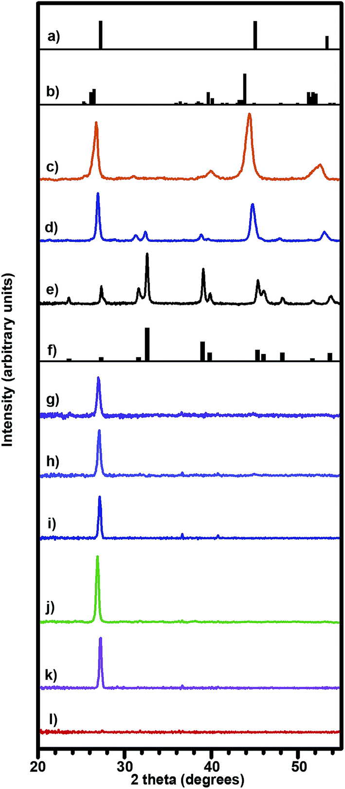 | ||
| Fig. 2 X-ray diffraction patterns of samples prepared in this work: (a) powder diffraction file for β-Cu2Se, file 00-027-1131, (b) powder diffraction file for α-Cu2Se, file 01-088-2043; diffraction patterns of bulk powders prepared using (c) the Cu2−xSe precursor, (d) a mixture of the Cu2−xSe and Cu2−xS precursors, and (e) the Cu2−xS precursor; (f) powder diffraction file for tetragonal Cu2S, file 01-072-1071; diffraction patterns of thin films prepared using the Cu2−xSe precursor at varying annealing temperatures of (g) 310 °C, (h) 350 °C, and (i) 390 °C; diffraction pattern of thin films with nominal compositions of (j) Cu1.83Ag0.009Se0.77S0.23, (k) Cu2.03Se0.52S0.48, and (l) Cu2.03S. | ||
The XRD pattern on the bulk Cu2−xS powder prepared from the Cu2−xS precursor exhibits the characteristic peaks of tetragonal Cu2−xS (Fig. 2e). In the case of the Cu2−xS thin film, no diffraction pattern peaks are observed (Fig. 2l). This means that either the thin film is amorphous or that the intensity of the thin film's tetragonal diffraction pattern is below our diffractometer's detection limit.
The bulk diffraction from the mixed Cu2−xSe–Cu2−xS precursor (Fig. 2d) was made with the same ratio as sample 6 in Table 1, and so we assume that it has a composition of Cu2.03Se0.52S0.48 as well. This diffraction pattern possesses characteristics of both compounds. It maintains the tetragonal diffraction pattern peaks from the Cu2−xS phase, but has the peaks shifted to lower 2 theta due to the larger atomic size of Se relative to S. In addition, the dominant peaks transition away from the tetragonal dominant peaks (32° and 39°) to the dominant Cu2−xSe peaks (27° and 45°), thereby confirming that the crystal structure of this sample also possesses characteristics of Cu2−xSe. The diffraction pattern of the thin film made with this precursor mixture resembles that of the other thin film samples. It exhibits texturing with a strong diffraction peak at 27.2° (Fig. 2k).
Prior literature36,49,50 demonstrates thermoelectric performance can be improved by doping Cu2−xX with Ag. Inspired by these results, we created Cu1.83Ag0.009Se0.77S0.23 samples by adding Ag2S precursor to the Cu2−xSe precursor and annealing at 350 °C. The X-ray diffraction pattern of this film is similar to the other films prepared with the Cu2−xSe precursor. It exhibits texturing and a strong diffraction peak at 26.9° (Fig. 2j).
Fig. 3 shows scanning electron micrographs of typical Cu2−xSeyS1−y and Ag-doped Cu2−xSeyS1−y thin films prepared in this work. Although these films were specular to the eye, the scanning electron micrographs show reveal nanoscale features and pores. The presence of these features and pores can be attributed to the mass loss that occurs during the precursors' physical transformation into Cu2−xSeyS1−y and Ag-doped Cu2−xSeyS1−y thin films.
 | ||
| Fig. 3 Scanning electron microscopy images of thin films prepared using the Cu2−xSe precursor at varying annealing temperatures of (a) 310 °C, (b) 350 °C, and (c) 390 °C; and thin films with nominal compositions of (d) Cu2.03S, (e) Cu2.03Se0.52S0.48, and (f) Cu1.83Ag0.009Se0.77S0.23. | ||
Having determined the salient structural and compositional features of Cu2−xSeyS1−y and Ag-doped Cu2−xSeyS1−y films prepared using EDA–EDT solvent mixtures, we proceeded to measure their thermoelectric properties. The energy conversion efficiency of a given thermoelectric material is given by its thermoelectric figure of merit, ZT. The thermoelectric figure of merit is given by the expression, ZT = S2σT/k, where S, σ, T, and k are the Seebeck coefficient, electrical conductivity, absolute temperature, and thermal conductivity. We measured the Seebeck coefficient, electrical conductivity, and thermal conductivity of our samples at room temperature using the steady-state slope method,38 van der Pauw method,38 and the 3ω method,39,40 respectively.
Fig. 4 shows the effect of precursor annealing temperature on the electrical conductivity, Seebeck coefficient, and thermal conductivity of thin films prepared with the Cu2−xSe precursor. We find that as the annealing temperature increases from 310 to 390 °C, the average Seebeck coefficient increases from 26 to 34 μV K−1 and the average electrical conductivity decreases from 1380 to 890 Ω−1 cm−1. The thermal conductivity of these samples was insensitive to annealing temperature and is approximately 0.6 W m−1 K−1. It is worth noting that Lin et al.30 measured the electrical conductivity of similarly prepared Cu2−xSe films that were annealed at 300 °C. Their value of 1168 Ω−1 cm−1 is comparable to our value of 1380 Ω−1 cm−1 obtained for samples annealed at 310 °C. Inspection of Fig. 4 also shows that the sample-to-sample variations in thermoelectric properties are non-negligible and in some cases can exceed the uncertainty of an individual measurement. The positive sign of the Seebeck coefficient indicates that our samples are p-type, which is typical for Cu2−xSe films where it is well known that Cu vacancies lead to holes.8,42 Our observation of an increasing Seebeck coefficient accompanied by a decreasing electrical conductivity is a well-known occurrence that arises from changes in charge carrier concentration. More specifically, it is known that decreasing carrier concentration in a semiconductor decreases electrical conductivity and increases Seebeck coefficient.4,51
 | ||
| Fig. 4 Room temperature properties of (a) electrical conductivity, (b) Seebeck coefficient, and (c) thermal conductivity of thin films prepared using the Cu2−xSe precursor at varying annealing temperatures. Each data point and error bar represents a distinct sample and the corresponding measurement uncertainty on that sample. | ||
We trace our observed electrical conductivity and Seebeck coefficient dependences on annealing temperature to stoichiometric changes in our samples. Inspection of our Rutherford backscattering spectroscopy shows that the amount of Cu vacancies (i.e., value of x) decreases from 0.22 to 0.06 as the annealing temperature is increased from 310 °C to 390 °C. Since Cu vacancies in Cu2−xSe lead to holes, this stoichiometric trend indicates that increasing annealing temperature leads to a decrease in hole concentration and consequently a decrease in electrical conductivity. Accompanying this decrease in hole concentration is an increase in Seebeck coefficient as dictated by the interplay of carrier concentration and Seebeck coefficient in thermoelectric materials.4,51
We also varied the Se:S ratio in our Cu2−xSeyS1−y by mixing in Cu2−xS precursor and annealing at 350 °C. Fig. 5 shows that as the Se:S ratio is decreased, the average Seebeck coefficient increased from 29 to 83 μV K−1 and the average electrical conductivity decreased from 1163 to 163 Ω−1 cm−1. This order of magnitude difference in electrical conductivity between samples prepared with the Cu2−xSe and Cu2−xS precursors is similar to that observed by Lin et al.30 Part of this change in electrical conductivity can be attributed to stoichiometry. The RBS data shows that the values of x in the samples prepared with the Cu2−xS precursor and Cu2−xS–Cu2−xSe precursor mixture is approximately zero. Consequently these samples should have less charge carriers than the samples prepared with the Cu2−xSe precursor. Our observed increase in Seebeck coefficient as the sample becomes more Cu2−xS rich is also consistent with this decrease in charge carrier concentration. It is also possible that changes in electronic band structure (e.g. band gap, inertial effective mass, density of states effective mass, crystallographic symmetry, etc.) could be contributing to these property trends, however our present data is insufficient to assess this possibility.
 | ||
| Fig. 5 Room temperature properties of (a) electrical conductivity and (b) Seebeck coefficient for varying Se:S ratios in samples of Cu2−xSeyS1−y composition. Each data point and error bar represents a distinct sample and the corresponding measurement uncertainty on that sample. Note that error bars on some data points are smaller than the data points themselves. | ||
We next turn our attention to the thermoelectric properties of our Ag-doped Cu2−xSeyS1−y prepared with a 350 °C annealing temperature, which results in a composition of Cu1.83Ag0.009Se0.77S0.23 (Table 2). Our efforts to Ag-dope our samples were motivated by the work of Brown et al.49 They studied Cu2Se and Cu1.97Ag0.03Se and found that Ag-doping increased structural entropy, which in turn dramatically increased S and slightly decreased σ around the α–β phase transition temperature region. They also found that doping Cu2Se with Ag broadened the temperature region of the continuous α–β phase transition, and caused the effect of increased structural entropy to be observed at lower temperatures. Lastly, they found that Ag-doping decreased thermal conductivity by increasing phonon scattering. We observe similar behaviour when comparing the thermoelectric properties of our Cu1.83Ag0.009Se0.77S0.23 and Cu1.89Se0.69S0.31 samples (Table 2 and Fig. 4). Ag-doping leads to an average Seebeck coefficient of 52 μV K−1, which represents an appreciable 80% increase over the non-Ag-doped samples. We note that the larger number of Cu vacancies and larger Se:S ratio in the doped samples relative to the non-doped samples cannot explain this increase in Seebeck coefficient. This is because we already showed that increases in Cu vacancies (Table 1 and Fig. 4) and increases in Se:S ratio (Fig. 5) both decrease Seebeck coefficient. Ag-doping also improves thermoelectric performance by decreasing thermal conductivity. We find that our Ag-doped samples have an average thermal conductivity of 0.43 W m−1 K−1, which is ∼30% lower than the non-Ag-doped samples. Sample-to-sample variations preclude us from definitively knowing if we also observe a small decrease in electrical conductivity with Ag-doping. While we speculate that the thermoelectric properties changes between our Cu1.83Ag0.009Se0.77S0.23 and Cu1.89Se0.69S0.31 samples have similar origins to the work by Brown et al.,49 this cannot be conclusively determined with the present data. First, our Ag-concentration is approximately 3 times lower than their work. We note that our Ag concentrations of 0.009 were near the solubility limit for the Cu2−xSe–Ag2S precursor mixture and so we could not attempt larger Ag concentrations for this reason. In addition, the behaviour observed by Brown et al.49 requires that the sample be near the α–β phase transition temperature region. This is true for the bulk powder sample prepared from the Cu2−xSe precursor because its XRD pattern exhibits both α- and β-phase peaks. However, the weak diffraction signal from our thin film samples cannot confirm the presence of both α- and β-phases in the thin film samples.
| Sample | Precursor annealing temperature (°C) | Seebeck coefficient (μV K−1) | Electrical conductivity (Ω−1 cm−1) | Thermal conductivity (W m−1 K−1) |
|---|---|---|---|---|
| Ag-1 | 350 | 44 ± 10% | 1027 ± 5% | — |
| Ag-2 | 350 | 49 ± 10% | 1134 ± 5% | — |
| Ag-3 | 350 | 61 ± 10% | 869 ± 5% | — |
| Ag-4 | 350 | — | — | 0.42 ± 15% |
| Ag-5 | 350 | — | — | 0.44 ± 15% |
| Average | — | 51 | 1010 | 0.43 |
Overall, the room temperature Seebeck coefficients, electrical conductivities, and thermal conductivities of our samples prepared using solution-phase processing of precursors yield similar values to Cu2−xSe alloys made via conventional thermoelectric material processing methods.8,35–37,49 We note that calculating the ZT of a thermoelectric material requires that all property measurements be performed along the same direction of the sample. This is not true in our case because our Seebeck coefficient and electrical conductivity measurements are in-plane measurements and our thermal conductivity measurements are cross-plane measurements. However, if one assumes that these properties are isotropic within our films, a ZT of 0.18 can be estimated for the Cu1.83Ag0.009Se0.77S0.23 sample. Although this is a modest value, it is important to note that the ZT of Cu2−xSe increases with temperature and large ZT values of 1.2–1.6 are commonly observed in the 600–700 °C range.8,35–37 Consequently, future high temperature measurements on the solution-phase processed materials in this work could be interesting.
4. Summary
We deposited metal chalcogenide semiconductor thin films using soluble precursors created with thiol–amine solvent mixtures and reported the first thermoelectric measurements on materials made in this manner. More specifically, we deposited and studied Cu2−xSeyS1−y and Ag-doped Cu2−xSeyS1−y thin films. We found that the precursor annealing temperature affects the metal:chalcogen ratio and leads to carrier concentration changes that affect Seebeck coefficient and electrical conductivity. We also found notable improvements in both Seebeck coefficient and thermal conductivity for our Ag-doped Cu2−xSeyS1−y. Overall, the room temperature thermoelectric properties of our solution-phase processed samples are comparable to those of Cu2−xSe alloys made via conventional thermoelectric material synthesis methods. Achieving parity between solution-phase processing and conventional processing is an important milestone and demonstrates the promise of this binary solvent approach as a solution-phase route to thermoelectric materials.
Acknowledgements
This work was supported by the National Science Foundation through award number DMR-1506829. We gratefully acknowledge the use of facilities within the LeRoy Eyring Center for Solid State Science and the Center for Solid State Electronics, both of which are located at Arizona State University. We also thank Barry Wilkens and Tim Karcher of the LeRoy Eyring Center for Solid State Science for performing Rutherford backscattering spectroscopy and thermogravimetric analysis measurements, respectively.References
- S. Chu and A. Majumdar, Nature, 2012, 488, 294–303 CrossRef CAS PubMed.
- S. K. Yee, S. LeBlanc, K. E. Goodson and C. Dames, Energy Environ. Sci., 2013, 6, 2561–2571 Search PubMed.
- C. J. Vineis, A. Shakouri, A. Majumdar and M. G. Kanatzidis, Adv. Mater., 2010, 22, 3970–3980 CrossRef CAS PubMed.
- A. Shakouri, Annu. Rev. Mater. Res., 2011, 41, 399–431 CrossRef CAS.
- K. Biswas, J. Q. He, I. D. Blum, C. I. Wu, T. P. Hogan, D. N. Seidman, V. P. Dravid and M. G. Kanatzidis, Nature, 2012, 489, 414–418 CrossRef CAS PubMed.
- L. D. Zhao, S. H. Lo, Y. S. Zhang, H. Sun, G. J. Tan, C. Uher, C. Wolverton, V. P. Dravid and M. G. Kanatzidis, Nature, 2014, 508, 373–376 CrossRef CAS PubMed.
- Y. Z. Pei, X. Y. Shi, A. LaLonde, H. Wang, L. D. Chen and G. J. Snyder, Nature, 2011, 473, 66–69 CrossRef CAS PubMed.
- H. Liu, X. Shi, F. Xu, L. Zhang, W. Zhang, L. Chen, Q. Li, C. Uher, T. Day and G. J. Snyder, Nat. Mater., 2012, 11, 422–425 CrossRef CAS PubMed.
- M. Ibáñez, Z. Luo, A. Genç, L. Piveteau, S. Ortega, D. Cadavid, O. Dobrozhan, Y. Liu, M. Nachtegaal, M. Zebarjadi, J. Arbiol, M. V. Kovalenko and A. Cabot, Nat. Commun., 2016, 7, 1–7 Search PubMed.
- G. H. Kim, L. Shao, K. Zhang and K. P. Pipe, Nat. Mater., 2013, 12, 719–723 CrossRef CAS PubMed.
- K. Peng, X. Lu, H. Zhan, S. Hui, X. Tang, G. Wang, J. Dai, C. Uher, G. Wang and X. Zhou, Energy Environ. Sci., 2016, 9, 454–460 CAS.
- X. Hu, P. Jood, M. Ohta, M. Kunii, K. Nagase, H. Nishiate, M. G. Kanatzidis and A. Yamamoto, Energy Environ. Sci., 2016, 9, 517–529 CAS.
- G. Bulman, P. Barletta, J. Lewis, N. Baldasaro, M. Manno, A. Bar-Cohen and B. Yang, Nat. Commun., 2016, 7, 10302–10307 CrossRef CAS PubMed.
- I. Chowdhury, R. Prasher, K. Lofgreen, G. Chrysler, S. Narasimhan, R. Mahajan, D. Koester, R. Alley and R. Venkatasubramanian, Nat. Nanotechnol., 2009, 4, 235–238 CrossRef CAS PubMed.
- C. Fu, S. Bai, Y. Liu, Y. Tang, X. Zhao, L. Chen and T. Zhu, Nat. Commun., 2015, 6, 1–7 Search PubMed.
- R. Y. Wang, J. P. Feser, X. Gu, K. M. Yu, R. A. Segalman, A. Majumdar, D. J. Milliron and J. J. Urban, Chem. Mater., 2010, 22, 1943–1945 CrossRef CAS.
- R. Y. Wang, J. P. Feser, J. S. Lee, D. V. Talapin, R. Segalman and A. Majumdar, Nano Lett., 2008, 8, 2283–2288 CrossRef CAS PubMed.
- K. C. See, J. P. Feser, C. E. Chen, A. Majumdar, J. J. Urban and R. A. Segalman, Nano Lett., 2010, 10, 4664–4667 CrossRef CAS PubMed.
- N. E. Coates, S. K. Yee, B. McCulloch, K. C. See, A. Majumdar, R. A. Segalman and J. J. Urban, Adv. Mater., 2013, 25, 1629–1633 CrossRef CAS PubMed.
- S. K. Yee, N. E. Coates, A. Majumdar, J. J. Urban and R. A. Segalman, Phys. Chem. Chem. Phys., 2013, 15, 4024–4032 RSC.
- S. Yee, T. Hendricks and S. LeBlanc, J. Electron. Mater., 2015, 45, 1751–1761 Search PubMed.
- S. LeBlanc, S. K. Yee, M. L. Scullin, C. Dames and K. E. Goodson, Renewable Sustainable Energy Rev., 2014, 32, 313–327 CrossRef CAS.
- A. K. Menon and S. K. Yee, J. Appl. Phys., 2016, 119, 055501 CrossRef.
- D. B. Mitzi, L. L. Kosbar, C. E. Murray, M. Copel and A. Afzali, Nature, 2004, 428, 299–303 CrossRef CAS PubMed.
- D. B. Mitzi, Adv. Mater., 2009, 21, 3141–3158 CrossRef CAS.
- D. J. Milliron, S. Raoux, R. Shelby and J. Jordan-Sweet, Nat. Mater., 2007, 6, 352–356 CrossRef CAS PubMed.
- D. H. Webber and R. L. Brutchey, J. Am. Chem. Soc., 2013, 135, 15722–15725 CrossRef CAS PubMed.
- J. J. Buckley, C. L. McCarthy, J. D. Pilar-Albaladejo, G. Rasul and R. L. Brutchey, Inorg. Chem., 2016, 55, 3175–3180 CrossRef CAS PubMed.
- C. L. McCarthy, D. H. Webber, E. C. Schueller and R. L. Brutchey, Angew. Chem., Int. Ed., 2015, 54, 8378–8381 CrossRef CAS PubMed.
- Z. Lin, Q. He, A. Yin, Y. Xu, C. Wang, M. Ding, H.-C. Cheng, B. Papandrea, Y. Huang and X. Duan, ACS Nano, 2015, 9, 4398–4405 CrossRef CAS PubMed.
- P. D. Antunez, D. A. Torelli, F. Yang, F. A. Rabuffetti, N. S. Lewis and R. L. Brutchey, Chem. Mater., 2014, 26, 5444–5446 CrossRef CAS.
- F. Liu, J. Zhu, Y. Li, J. Wei, M. Lv, Y. Xu, L. Zhou, L. Hu and S. Dai, J. Power Sources, 2015, 292, 7–14 CrossRef CAS.
- R. Zhang, S. Cho, D. G. Lim, X. Hu, E. A. Stach, C. A. Handwerker and R. Agrawal, Chem. Commun., 2016, 52, 5007–5010 RSC.
- D. Zhao, Q. Tian, Z. Zhou, G. Wang, Y. Meng, D. Kou, W. Zhou, D. Pan and S. Wu, J. Mater. Chem. A, 2015, 3, 19263–19267 CAS.
- K. Tyagi, B. Gahtori, S. Bathula, M. Jayasimhadri, N. K. Singh, S. Sharma, D. Haranath, A. K. Srivastava and A. Dhar, J. Phys. Chem. Solids, 2015, 81, 100–105 CrossRef CAS.
- S. Ballikaya, H. Chi, J. R. Salvador and C. Uher, J. Mater. Chem. A, 2013, 1, 12478–12487 CAS.
- B. Yu, W. Liu, S. Chen, H. Wang, H. Wang, G. Chen and Z. Ren, Nano Energy, 2012, 1, 472–478 CrossRef CAS.
- K. A. Borup, J. de Boor, H. Wang, F. Drymiotis, F. Gascoin, X. Shi, L. Chen, M. I. Fedorov, E. Müller, B. B. Iversen and G. J. Snyder, Energy Environ. Sci., 2015, 8, 423–435 CAS.
- S. M. Lee and D. G. Cahill, J. Appl. Phys., 1997, 81, 2590–2595 CrossRef CAS.
- D. G. Cahill, Rev. Sci. Instrum., 1990, 61, 802–808 CrossRef CAS.
- T. Borca-Tasciuc, A. R. Kumar and G. Chen, Rev. Sci. Instrum., 2001, 72, 2139–2147 CrossRef CAS.
- T. Ohtani, Y. Tachibana, J. Ogura, T. Miyake, Y. Okada and Y. Yokota, J. Alloys Compd., 1998, 279, 136–141 CrossRef CAS.
- X.-X. Xiao, W.-J. Xie, X.-F. Tang and Q.-J. Zhang, Chin. Phys. B, 2011, 20, 087201 CrossRef.
- A. Tonejc, J. Mater. Sci., 1980, 15, 3090–3094 CrossRef CAS.
- Z. Ogorelec and B. Celustka, J. Phys. Chem. Solids, 1966, 27, 615 CrossRef CAS.
- R. M. Murray and R. D. Heyding, Can. J. Chem., 1975, 53, 878–887 CrossRef CAS.
- F. El Akkad, B. Mansour and T. Hendaya, Mater. Res. Bull., 1981, 16, 535–539 CrossRef CAS.
- B. Celustka and Z. Ogorelec, J. Phys. Chem. Solids, 1971, 32, 1449 CrossRef CAS.
- D. R. Brown, T. Day, K. A. Borup, S. Christensen, B. B. Iversen and G. J. Snyder, APL Mater., 2013, 1, 052107 CrossRef.
- T. W. Day, W. G. Zeier, D. R. Brown, B. C. Melot and G. J. Snyder, Appl. Phys. Lett., 2014, 105, 172103 CrossRef.
- G. J. Snyder and E. S. Toberer, Nat. Mater., 2008, 7, 105–114 CrossRef CAS PubMed.
Footnote |
| † Electronic supplementary information (ESI) available: Temperature calibration data that relates the hotplate set temperature to the substrate surface temperature, additional scanning electron microscope images, and Rutherford backscattering spectroscopy data. See DOI: 10.1039/c6ra15929j |
| This journal is © The Royal Society of Chemistry 2016 |